INDUSTRIAL I/O PACK SERIES APCe8650
PCI BUS CARRIER BOARD
Acromag, Inc. Tel: 248-295-0310
- 11 -
www.acromag.com
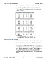
“B” is on the component side of the carrier board while “A” is on the solder
side. Connector “gold finger” numbers increase with distance from the
bracket end of the printed circuit board.
Refer to the PCI Express bus specification for additional information on the
PCI Express bus signals
Table 2-2 PCIe Bus P1 CONNECTIONS
Signal
Pin
Pin
Signal
+12V
B01
A01
PRSNT1*
+12V
B02
A02
+12V
+12V
B03
A03
+12V
GND
B04
A04
GND
SMCLK
B05
A05
TCK
SMDAT
B06
A06
TDI
GND
B07
A07
TDO
+3.3V
B08
A08
TMS
TRST*
B09
A09
+3.3V
+3.3Vaux
B10
A10
+3.3V
WAKE*
B11
A11
PERST*
RSVD
B12
A12
GND
GND
B13
A13
REFCLKp
Tx0p
B14
A14
REFCLKn
Tx0n
B15
A15
GND
GND
B16
A16
Rx0p
PRSNT2*
B17
A17
Rx0n
GND
B18
A18
GND
Notes (Table 2-2):
1.
Asterisk (*) is used to indicate an active-low signal.
2.
BOLD ITALIC Logic Lines are NOT USED by the carrier board.
FIELD GROUNDING CONSIDERATIONS
Carrier boards are designed with passive filters on each supply line to each IP
module. This provides maximum filtering and signal decoupling between the
IP modules and the carrier board. However, the boards are considered non-
isolated, since there is electrical continuity between the PCIe bus and the IP
grounds. Therefore, unless isolation is provided on the IP module itself, the
field I/O connections are not isolated from the PCI bus. Care should be taken
in designing installations without isolation to avoid ground loops and noise
pickup. This is particularly important for analog I/O applications when a high
level of accuracy/resolution is needed (12-bits or more). Contact your
Acromag representative for information on our many isolated signal
conditioning products that could be used to interface to the IP input/output
modules.


