Series AVME9125 VMEbus 6U Analog Input Board
___________________________________________________________________________________________
- 14 -
When the board recognizes an interrupt acknowledge cycle on
the VMEbus, it checks for a match of the interrupt request. If an
interrupt is not pending or the interrupt level does not match, it will
pass the acknowledgment signal along, without consuming it. If
there is a match, the board will initiate an acknowledgment cycle
and supply the interrupt vector during the cycle.
Interrupt Configuration Example
1. Write interrupt vector to board address 45H.
2. Write to the Interrupt Level in the control register to program
the desired interrupt level per bits 2,1,0. Also enable the
interrupt type in control register bits 12 and 13.
Sequence of Events For an Interrupt
1. The AVME9125 asserts an interrupt request by asserting
IRQx* as programmed in the interrupt level bits of the control
register.
2. The VMEbus host (interrupt handler) asserts IACK* and the
level of the interrupt it is seeking on A01-A03.
3. When the asserted VMEbus IACKIN* signal (daisy-chained) is
passed to the AVME9125, the board will check if the level
requested matches that specified by the host. If so, the board
will put the interrupt vector on the data bus (D00-D07 if an D08
(O) interrupter or D00-D15 if a D16 interrupter), and asserts
DTACK* to the system master.
4. The host uses the vector as a pointer to an interrupt handler to
execute and begins its execution.
5. Example of Generic Interrupt Handler Actions:
A. Take any specific action required to remove the interrupt
request at its source.
6. If the interrupt stimulus has been removed and no other
interrupts are pending, the interrupt cycle is completed (i.e. the
board negates its interrupt request).
A. If another interrupt is pending, then the interrupt request
(IRQx*) will remain asserted. This will start a new interrupt
cycle.
4.0 THEORY OF OPERATION
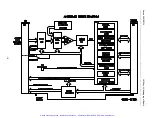
This section describes the basic functionality of the circuitry
used on the AVME9125 board. Refer to the Block Diagram shown
in the Drawing 4501-678 as you review this material.
AVME9125 BOARD OVERVIEW
The AVME9125 board is a VMEbus slave board providing up
to 32 differential analog to digital input channels with expander
board EXP9125. The board’s VMEbus interface allows an
intelligent single board computer (VMEbus Master) to monitor 32
analog channels.
VMEbus Interface
The board’s VMEbus interface is used to program and monitor
and board’s registers for configuration and control of the board’s
documented modes of operation (see section 3).
The VMEbus interface is implemented in the logic of a Field
Programmable Gate-Array (FPGA). The FPGA implements
VMEbus specification revision C.1 as an interrupting slave
including the following data transfers types.
•
A16, D16/D08(O) Short I/O Access
The board’s VMEbus data transfer rates are typically:
•
800ns for accesses to the AVME9125 board registers.
The board’s FPGA monitors the base address jumper setting
which is jumperable on 256 byte boundaries in the VMEbus Short
I/O (A16) Address Space. When the selected base address
matches the (A16) address provided by the VMEbus master, the
FPGA controls and implements the required bus transfer allowing
communication with the AVME9125 board’s registers.
Board Registers and Control Logic
All logic to control data acquisition is imbedded in two board
FPGAs. One FPGA is dedicated to the VMEbus interface while
the other FPGA handles control of data acquisition. The data
acquisition control logic performs the following:
•
Controls the channel multiplexers based upon start and
end channel values.
•
Controls data conversion at the A/D Converter based on
one of four different scan modes of operation.
•
Controls data transfer from the A/D Converter to the
FPGA’s 16-bit serial shift register.
•
Controls and updates the Mail Box buffer, New Data
register, and Missed Data register.
•
Stops data acquisition for Single Cycle Scan modes.
•
Controls the interval between data conversions.
•
Issues interrupt requests to the system master.
INTERNAL CHANNEL POINTERS
Internal counters in the FPGA are used as pointers to: control
the multiplexers for selection of the current channel’s analog signal
and control update of the Mail Box RAM buffer. The start channel
register controls the value at which these counters start and the
end value register controls the maximum channel number which is
reached.
In the continuous modes of operation these counters
continuously cycle, in sequential order, from the defined start
value to the defined end value. When the continuous mode of
operation is halted by disabling the scan mode via the control
register, the internal hardware counter remains at the count value
reached when halted. Upon start of a new scan mode, via the
software start convert bit, the internal pointers are reinitialized.
Thus, the first channel converted, upon restart of data
conversions, will correspond to that set in the start value register.
A 16-bit serial shift register is implemented in the board’s
FPGA. This serial shift register interfaces to the A/D Converter. A
clock signal provided by the converter is used to serially shift the
new data from the converter to the FPGA’s 16-bit serial shift
register. Use of the converter’s clock signal (instead of an external
clock) minimizes the danger of digital noise feeding through and
corrupting the results of a conversion in process.
The converted data serially shifted, from the A/D Converter to
the FPGA, represents the analog signal digitized in the previous
convert cycle. That is, the A/D Converter transfers digitized
analog input data to the FPGA one convert cycle after it has been
digitized. Serially shifting of the 16-bits of digitized data to the
FPGA and then writing to the Mail Box buffer is completed 10.5
µ
seconds after start of the convert cycle.
Artisan Technology Group - Quality Instrumentation ... Guaranteed | (888) 88-SOURCE | www.artisantg.com


