Series AVME9125 VMEbus 6U Analog Input Board
___________________________________________________________________________________________
- 4 -
For repairs to a product damaged in shipment, refer to the
Acromag Service Policy to obtain return instructions. It is
suggested that salvageable shipping cartons and packing material
be saved for future use in the event the product must be shipped.
This board is physically protected
with packing material and electrically
protected with an anti static bag
during shipment. It is recommended
that the board be visually inspected
for evidence of mishandling prior to
applying power.
The board utilizes static sensitive
components and should only be
handled at a static-safe workstation.
CARD CAGE CONSIDERATIONS
Refer to the specifications for loading and power
requirements. Be sure that the system power supplies are able to
accommodate the power requirements of this board, within the
voltage tolerances specified.
IMPORTANT: Adequate air circulation must be provided to
prevent a temperature rise above the maximum operating
temperature.
Adequate air circulation must be provided to prevent a
temperature rise above the maximum operating temperature and
to prolong the life of the electronics. If the installation is in an
industrial environment and the board is exposed to environmental
air, careful consideration should be given to air-filtering.
BOARD CONFIGURATION
The board may be configured for different applications. All
possible configuration settings will be discussed in the following
Sections.
VMEbus INTERFACE CONFIGURATION
The board is shipped from the factory configured as follows:
•
With VMEbus Short I/O Base Address of 00XXH. Board will
respond to both Address Modifiers 29H (short non-privileged
I/O) and 2DH (short supervisory I/O). Registers on the board
will be accessible.
•
Programmable software registers default to interrupt
requests-disabled and VMEbus interrupt level-none.
Address Decode Jumper Configuration
The AVME9125 board interfaces with the VMEbus as a 256
byte block of address locations in the VMEbus short I/O address
space (refer to Section 3 for memory map details). J1 decodes
the eight most significant address lines A8 through A15 to provide
256 byte segments of address space. The configuration of the
jumpers for different base address locations is shown in Table 2.1.
"IN" means that the pins are shorted together with a shorting clip.
"OUT" indicates that the clip has been removed. The jumper
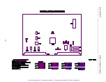
locations are shown in Drawing 4501-679.
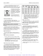
Table 2.1: Address Decode Jumper Selections (J1 Pins)
Addr
Line
Jumper
Pins
Base
Addr
00XXh
Base
Addr
07XXh
Base
Addr
1BXXh
Base
Addr
FFXXh
1
A15
15-16
OUT
OUT
OUT
IN
A14
13-14
OUT
OUT
OUT
IN
A13
11-12
OUT
OUT
OUT
IN
A12
09-10
OUT
OUT
IN
IN
A11
07-08
OUT
OUT
IN
IN
A10
05-06
OUT
IN
OUT
IN
A09
03-04
OUT
IN
IN
IN
A08
01-02
OUT
IN
IN
IN
1) When the board is shipped from the factory, it is configured
for default hardware jumper configuration of 00XX hex.
2) Consult your host CPU manual for detailed information about
addressing the VMEbus short I/O (A16, 16-bit) space. In
many cases, CPU's utilizing 24-bit addressing will start the
16-bit address at FF0000 (Hex), and 32-bit CPU's at
FFFF0000 (Hex).
VMEbus Address Modifiers
No hardware jumper configuration is needed. The AVME9125
board will respond to both address modifiers 29H and 2DH in the
VMEbus short I/O space. This means that both short supervisory
and short non-privileged accesses are supported.
Interrupt Configuration
No hardware jumper configuration is required. All interrupt
enabling, status, and VMEbus interrupt level selections are
configured via programmable registers on the AVME9125 board
(see Section 3 for programming details).
VMEbus Connections
The AVME9125 communicates with the Host computer in the
short I/O addressing space on the P1 connector. The P2
connector is used to receive 16 differential analog input signals for
analog to digital conversion. In addition, the P2 connector is used
to communicate with the Expander card (EXP-9125) for interface
to an additional 16 differential analog signals.
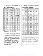
Table 2.2 indicates the pin assignments for the VMEbus
signals at the P1 connector. The P1 connector is the upper rear
connector on the AVME9125 board, as viewed from the front. The
connector consists of 32 rows of three pins labeled A, B, and C.
Pin A1 is located at the upper left hand corner of the connector if
the board is viewed from the front.
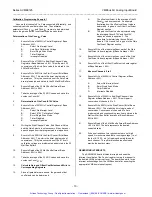
VMEbus connector P2 is the lower rear connector on the
AVME9125 board, as viewed from the front. Table 2.3 indicates
the pin assignments for the signals of the P2 connector.
Refer to the VMEbus specification for additional information on
the VMEbus signals.
Artisan Technology Group - Quality Instrumentation ... Guaranteed | (888) 88-SOURCE | www.artisantg.com


