AXM-
A75 User’s Manual
Multifunction I/O Mezzanine Board
_____________________________________________________________________________________
- 24 -
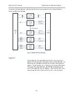
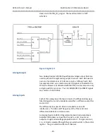
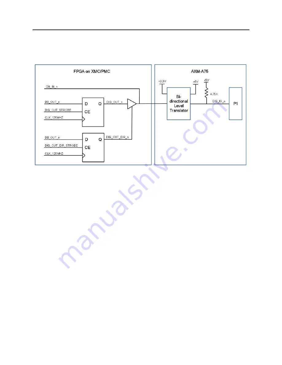
driven onto the DIG_IO_n signal. The level translator is a NXP
GTL2010.
Figure 2 Digital I/O
Analog Outputs
Two Analog Devices AD5764R quad bipolar voltage output DACs are
used to provide the eight analog output channels. Each DAC uses its
own on-chip reference as its reference source. Although each DAC
has separate clock, sync, load and serial I/O signals connected to the
FPGA, the firmware as delivered with the EDK provides access to only
a single quad DAC at a time. The CLR, BIN2SCOMP and RESET signals
are common to both DACs.
Analog Inputs
Each of the analog input channels consists of a differential low pass
filter followed by an instrumentation amplifier, a difference amplifier
and an ADC.
The differential low pass RC filter is intended to reduce RF
interference. The 3db cutoff frequency of the filter is 421 kHz
differential, 8.84 MHz common mode.
An Analog Devices AD8251 Programmable Gain (Instrumentation)
Amplifier (PGA) takes as input the channel’s + and
- inputs and
outputs a single ended voltage proportional to it. The gain can be 1,
2, 4, or 8 and is selected through the gain selection bits in the control
register. The gain selection affects all channels.


