Model DT233-0600
Dual Two-Wire mV/TC Input Transmitters
Acromag, Inc. Tel: 248-295-0880
- 38 -
http://www.acromag.com
- 38 -
https://www.acromag.com
Inputs (each)
…
For simplification,
the raw internal A/D counts indicated in Table 3 are normalized to
±25000/15.5 bits for
100% (bipolar ranges), or 0-25000/14.5 bits for 0-100%
(unipolar ranges). The effective I/O resolution of your transmitter will be the lowest
of either the input A/D, or the linearization conversion to temperature (which
resolves to 0.05°C on TC inputs), its normalized value, or the output DAC (1 part in
43690 for 4-20mA). The output resolution is greater than the input resolution and
will not be a limiting factor, except for the ±1V range. In most cases or for small
input spans, input resolution will be dominated by the 0.05°C temperature resolution
of the thermocouple linearizer.
Outputs (Each)
Output Range:
Output is 4 to 20mA DC nominal, linear with TC sensor temperature
or millivolt signal applied at the input terminals. Output has under-range capability
down to 3.5mA, and over-range up to 24mA, depending on input range selected and
I/O scaling. With Namur NE 43 limits selected, the linear under-range limit is ~3.7mA,
and linear over-range limit is ~20.7mA, with fault detents set outside the linear signal
range at ~3.5mA (downscale) and ≥ ~21mA
(upscale).
Output Accuracy:
Accuracy is typically better than
0.05% of span (
0.1% Max) for
nominal input ranges. Relative accuracy varies with calibrated input and output
span, and scaling. Accuracy includes the combined effects of repeatability, terminal
point conformity, and linearization, but does not include sensor error.
Output Ripple/Noise:
Less than
0.1% of output span.
Note
–
High Speed Acquisition: Additional filtering at the loop load is recommended
for sensitive applications with high-speed acquisition rates. For excessive 60Hz
supply ripple, a 1uF or larger capacitor is recommended at the load. High frequency
noise may be reduced or eliminated by placing a 0.1uF or 0.01uF capacitor directly
across the loop load (this can also raise RF immunity).
Output Ambient Temperature Effect:
The combined effect of zero and span drift
over temperature is better than ±0.008% of span per
C (
80ppm/
C) over the full
ambient temperature range for reference test conditions (see Input Specifications).
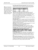
Output DAC Resolution:
Each output includes a 16-bit current DAC (Texas
Instruments DAC161S997RGH) with current set to 24mA*COUNT/65536 (see Table
4). Its 4-20mA output will yield an output resolution of 54613-10923, or 1 part in
43690. Linear range limits are programmable or set to Namur limits near ~3.7mA
(low) & ~20.7mA (upper), allowing you to discern an upscale or downscale lead break
condition from the linear operating range. The effective I/O resolution of this
transmitter will be the lowest of either the input, normalization, or the output.
Table 4: Output DAC Current Level & Digital DAC Count
I-LOOP = 24mA*COUNT/65536
COUNT = 65536*I-LOOP/24mA
3.7mA
10103
4.0mA
10923
12mA
32768
20mA
54613
20.7mA
56525
23.9996mA
65535


