SERIES IOS-320 I/O SERVER MODULE 12-BIT HIGH DENSITY ANALOG INPUT BOARD
__________________________________________________________________________________________
- 9 -
Acromag, Inc. Tel:248-295-0310 Fax:248-624-9234 Email:solutions@acromag.com http://www.acromag.com
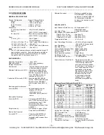
Uncalibrated Performance
The uncalibrated performance is affected by two primary
error sources. These are the Programmable Gain Amplifier
(PGA) and the Analog to Digital Converter (ADC). The
untrimmed PGA and ADC have the following performance:
PGA206AU @25oC:
Linearity Error is 0.005% Maximum (i.e. 1/4 LSB).
Offset Error RTI is 1mv Typical; 2.5mV Maximum.
Gain Error is 0.01% typical, 0.1% maximum for all gains.
(ADC) ADS8508 @25oC:
Linearity Error is 0.5 LSB Maximum.
Unipolar Zero Error is 5 mV Maximum.
Bipolar Zero Error is 1 mV Maximum.
Full Scale Calibration Error is 0.5% of span, Maximum.
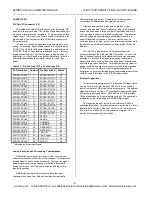
Table 3.3: Maximum Overall Uncalibrated Error at 25 C
Input Range
(Volts)
PGA
Gain
ADC
Range
(Volts)
Max
Offset
Error
( LSB)
Max
Gain
Error
( LSB
)
-5 to +5
1
-5 to +5
1.43
22.53
-2.5 to +2.5
2
"
“
"
-1.25 to +1.25
4
"
“
"
-0.625 to
+0.625
8
"
“
"
-10 to +10
1
-10 to +10
0.72
"
-5 to +5
2
"
“
"
-2.5 to +2.5
4
"
“
"
-1.25 to +1.25
8
"
“
"
0 to +10
1
0 to +10
3.08
24.58
0 to +5
2
"
“
"
0 to +2.5
4
"
“
"
0 to +1.25
8
"
“
"
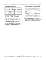
Note that the worst case non-linearity error is 0.75 LSB (the
sum of the ½ LSB non-linearity of the ADC and the ¼ LSB
non-linearity of the PGA).
Calibrated Performance
Very accurate calibration of the IOS-320 can be
accomplished by using calibration voltages present on the board.
The four voltages and the analog ground reference are used to
determine the endpoints of a straight line which defines the
analog input characteristic. The calibration voltages are precisely
adjusted at the factory to provide optimum performance, as
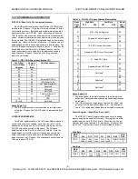
detailed in the following table:
Calibration
Signal
Ideal
Value
(Volts)
Maximum
Tolerance
@25oC (Volts)
Maximum
Temperature
Drift (ppm/oC)
Auto Zero
0.0000
0.0002
0
CAL0
4.9000
0.0005
15
CAL1
2.4500
0.0005
20*
CAL2
1.2250
0.0004
"
CAL3
0.6125
0.0002
"
* Worst case temperature drift is the sum of the 15 ppm/oC drift
of the calibration voltage reference plus the 5 ppm/oC drift of
the resistors in the voltage divider.
The calibration voltages are used with the auto zero signal to
find two points that determine the straight line characteristic of
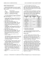
the analog front end for a particular range. The recommended
calibration voltage selection for each range is summarized in the
following table:
Table 3.4: Recommended Calib. Voltages For Input Ranges
Input
Range
(Volts)
PGA
Gain
ADC
Range
(Volts)
Rec. Low
Calib.
Voltage
"VoltCALLO"
(Volts)
Rec. High
Calib.
Voltage
"VoltCALHI"
(Volts)
-5 to
+5
1
-5 to +5
0.0000 (A. Z.)
4.9000 (CAL0)
-2.5 to
+2.5
2
"
"
2.4500 (CAL1)
-1.25 to
+1.25
4
"
"
1.2250 (CAL2)
-0.625 to
+0.625
8
"
"
0.6125 (CAL3)
-10 to
+10
1
-10 to
+10
"
4.9000 (CAL0)
-5 to
+5
2
"
"
4.9000 (CAL0)
-2.5 to
+2.5
4
"
"
2.4500 (CAL1)
-1.25 to
+1.25
8
"
"
1.2250 (CAL2)
0 to
+10
1
0 to +10
0.6125 (CAL3)
4.9000 (CAL0)
0 to
+5
2
"
"
4.9000 (CAL0)
0 to
+2.5
4
"
"
2.4500 (CAL1)
0 to
+1.25
8
"
"
1.2250 (CAL2)

