SERIES IP1K110 INDUSTRIAL I/O PACK RECONFIGURABLE DIGITAL I/O MODULE
__________________________________________________________________________________________
- 6 -
Acromag, Inc. Tel:248-295-0310 Fax:248-624-9234 Email:solutions@acromag.com
http://www.acromag.com
3.0 PROGRAMMING INFORMATION
This board is addressable in the Industrial Pack I/O space to
control in-system configuration of an Altera FPGA. After the
Altera FPGA is configured the IP I/O space is used to control
data transfer, and steering logic of the mix of up to 24 EIA
RS485/RS422 serial channels and up to 48 digital TTL channels.
The IP1K110 includes a 64K x 16 static memory device and clock
generator chip which are also both accessed via the IP bus
interface through the Altera FPGA.
Upon an initial power reset the IP1K110 responds to IP bus
ID space accesses and I/O space accesses. The ID space
accesses allow board identification. The I/O space accesses
allow configuration of the Altera FPGA. After the Altera FPGA is
successfully configured, the IP bus interface functions as defined
by the logic program of the Altera FPGA. The IP1K110 in-system
configuration logic will be disabled by the newly configured Altera
FPGA.
IN-SYSTEM CONFIGURATION ADDRESS MAPS
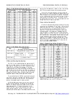
The I/O space address map for the IP1K110 when in
configuration mode is as shown in Table 3.1. The IP1K110 is in
configuration mode upon system power up and when the
Config_Enable line on pin168 of the Altera FPGA is a logic high.
The Config_Enable line must be held low by the Altera FPGA
after successful configuration to disable configuration mode.
Note that upon initial power up a pull-up resistor connected to pin
168 of the Altera FPGA keeps the IP1K110 in configuration
mode. After the FPGA is configured, the internal logic of the
FPGA must pull this resistor down to a logic low to disable
configuration mode.
If you have a configured FPGA and then wanted to re-
configure the FPGA again you must enable configuration mode.
This is accomplished by driving pin 168 of the FPGA to a logic
high level via control register bit-0. If you change your mind and
want to return control back to the FPGA an IP bus reset can be
used to clear or drive pin 168 to a logic low level (see example
VHDL file). Note that the Altera FPGA must not drive the IP bus
data lines or the ACK
∗
signal after you return to configuration
mode from a configured FPGA. Also, IP bus write cycles must
be disabled from changing the registers of your configured FPGA
while in configuration mode.
Table 3.1: IP1K110 Configuration Address Map (IO Space)
EVEN
Base
Addr.+
EVEN Byte
D15 D08
ODD Byte
D07 D00
ODD
Base
Addr.
+
00
Not Used
Control/Status
Register
01
02
Not Used
Configuration Data
Register
03
IP1K110 Configuration Procedure
The IP1K110 implements configuration of the Altera FPGA
over the IP bus interface. The IP1K110 uses the Altera passive
parallel asynchronous scheme with the IP bus serving as the
download path. Thus, download and configuration is
implemented with no special hardware or cables.
An example program written in C and available from
Acromag, implements configuration of the IP1K110 over the IP
bus. The program requires the configuration file to be in the Intel
Hex format.
Using the Altera MAX+PLUS II software, you can generate
the required hex file as follows.
1)
In the MAX+PLUS II Compiler, choose the Convert
SRAM Object Files command.
2)
In the Convert SRAM Object Files dialog box, select
your SOF file and then select .hex in the File Format
box. Click OK.
For further information on generating hex files refer to the
documentation supplied with the EDK.
The steps implemented by the example C program are listed
next.
1.
Start in configuration mode. Upon system power-up the
IP1K110 is in configuration mode. If the Altera FPGA is
currently configured and operational, configuration mode
can be entered by driving pin 168 of the Altera FPGA to
a logic high via the control register bit-0. Pin 168 is the
Config_Enable signal which upon system power-up is
held high by a pullup resistor.
2.
You can verify that you are in configuration mode by
reading ID space at base a 0Bhex. The byte
read will be 42hex when in configuration mode and
43hex when in user mode.
3.
Configuration is started by setting bit-0 of the control
register, at base a 01H, to a logic high.
4.
This same register bit-0 must be read next. When read
as a logic high software can proceed to the data transfer
phase. A polling method should be used here since this
bit will not be read high until 5
µ
seconds after the control
bit is set high.
5.
The status of the Altera FPGA during configuration can
be monitored via the Status register at base a
01H. Bit-1 monitors the Altera nStatus signal which
must remain high during configuration. Bit-2 of the
Status register reflects the Altera FPGA CONF_DONE
signal. The CONF_DONE signal must remain at a logic
low until configuration has completed.
6.
Write program data, one byte at a time, to the
Configuration Data register at base a 03H.
7.
Upon successful configuration, control of the IP bus will
automatically be switched to user mode and the Altera
FPGA will have control of the IP bus interface. This is
accomplished by the newly configured Altera FPGA
taking control of the Config_Enable signal (pin 168) and
pulling this signal low.
Altera FPGA Logic Requirements
There are two main modes of operation on the IP1K110
module: configuration mode and user mode. The IP1K110
powers up in configuration mode and remains in that mode until
the Altera FPGA is successfully configured. Once the Altera
FPGA is successfully configured, control is automatically
transferred to user mode and the Altera FPGA has control of the
IP bus interface. In order to implement this transition, the
following requirements must be respected by the Altera FPGA.
1.
Pin 168 of the Altera FPGA is reserved as an
Config_Enable control. When Pin 168 is driven low the
IP1K110 is in user mode and the Altera FPGA has
control of the IP bus interface. When Pin 168
(Config_Enable) is driven high the IP1K110 is in
configuration mode.


