background image

SERIES IP220 INDUSTRIAL I/O PACK 

1

2

-BIT HIGH-DENSITY ANALOG OUTPUT MODULE

Base

A

(Hex)

Even Byte

D15 

D

0

8

Odd Byte

D07  D O O

00

(W) - DAC Channel 0

02

(W) - DAC Channel 1

04

(W) - DAC Channel 2

06

(W) - DAC Channel 3

08

(W) - DAC Channel 4

OA

(W) - DAC Channel 5

OC

(W) - DAC Channel 6

OE

(W) - DAC Channel 7

10

(W) - DAC Channel 82

12

W) - DAC Channel 92

14

(W) - DAC Channel 102

16

(W) - DAC Channel 112

18

(W) - DAC Channel 122

1A

(W) - DAC Channel 132

1C

(W) - DAC Channel 142

1E

(W) - DAC Channel 152

20

(W) - Transparent Mode

22

(W)- Simultaneous Mode

24

(W) • Simultaneous Output Trigger

26

.1.

3E

NOT USED'

40

(R)-CHO Offset Error

42

(R)-CHO Gain Error

44

(R)-CH1 Offset Error

46

(R)-CH1 Gain Error

48

(R)-CH2 Offset Error

4A

(R)-CH2 Gain Error

4C

(R)-CH3 Offset Error

4E

(R)-CH3 Gain Error

50

(R)-CH4 Offset Error

52

(R)-CH4 Gain Error

54

(R)-CH5 Offset Error

56

(R)-CH5 Gain Error

58

(R)-CH6 Offset Error

5A

(R)-CH6 Gain Error

5C

(R)-CH7 Offset Error

5E

(R)-CH7 Gain Error

60

(R)-CH8 Offset Error2

62

(R)-CH8 Gain Error2

64

(R)-CH9 Offset Error2

66

(R)-CH9 Gain Error'

68

(R)-CH10 Offset Error2

6A

(R)-CH10 Gain Error2

6C

(R)-CH11 Offset Error2

6E

(R)-CH11 Gain Error`

70

(R)-CH12 Offset Error`

72

(R)-CH12 Gain Error2

74

(R)-CH13 Offset Error2

76

(R)-CH13 Gain Error2

78

(R)-CH14 Offset Error'

7A

(R)-CH14 Gain Error2

7C

(R)-CH15 Offset Error2

7E

(R)-CH15 Gain Error`

Hex Offset

From ID

PROM Base

Address

ASCII

Character

Equivalent

Numeric

Value

(Hex)

Field

Description

01

I

49

All IP's have

'IPAC'

03

P

50

05

A

41

07

C

43

09

A3

Acromag ID

Code

OB

22 IP220-16

23 IP220-8

IP Model

Code

OD

00

Not Used

(Revision)

OF

00

Reserved

11

00

Not Used

(Driver ID Low

Byte)

13

00

Not Used
(Driver ID

High Byte)

15

OC

Total Number

of ID PROM

Bytes

17

55 IP220-16

34 IP220-8

CRC

19 to 3F

yy

Not Used

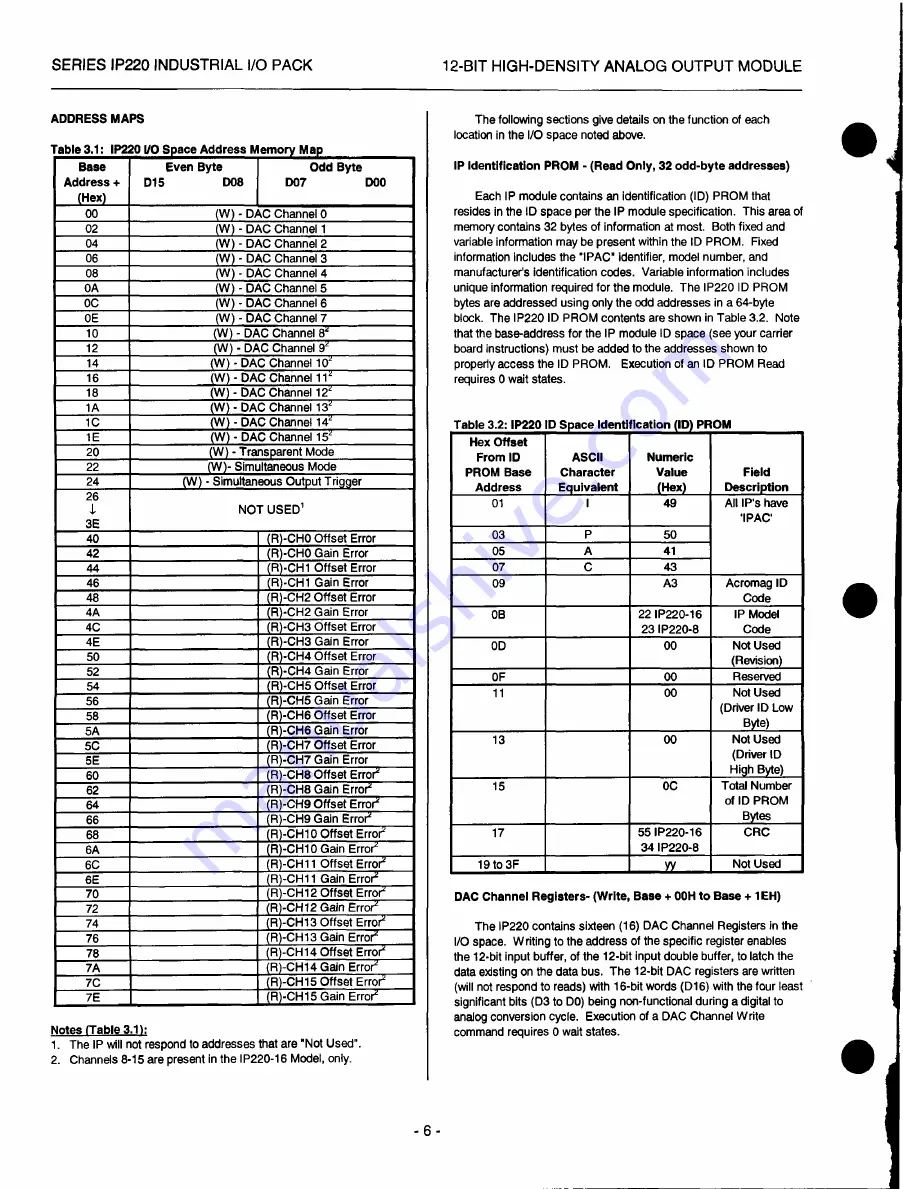
ADDRESS MAPS

Table 3.1: IP220 I/O Space Address Memory Ma

Notes (Table 3.1):
1. 

The IP will not respond to addresses that are "Not Used".

2. Channels 8-15 are present in the IP220-16 Model, only.

The following sections give details on the function of each

location in the I/O space noted above.

IP Identification PROM - (Read Only, 32 odd-byte addresses)

Each IP module contains an identification (ID) PROM that

resides in the ID space per the IP module specification. This area of
memory contains 32 bytes of information at most. Both fixed and
variable information may be present within the ID PROM. Fixed
information includes the "IPAC" identifier, model number, and
manufacturer's identification codes. Variable information includes
unique information required for the module. The IP220 ID PROM
bytes are addressed using only the odd addresses in a 64-byte
block. The IP220 ID PROM contents are shown in Table 3.2. Note
that the base-address for the IP module ID space (see your carrier
board instructions) must be added to the addresses shown to
properly access the ID PROM. Execution of an ID PROM Read
requires 0 wait states.

Table 3.2: IP220 D Space Identi ication (ID) PROM

DAC Channel Registers- (Write, Base + OOH to Base + lEH)

The 

IP220 contains sixteen (16) DAC Channel Registers in the

I/O space. Writing to the address of the specific register enables

the 12-bit input buffer, of the 12-bit input double buffer, to latch the
data existing on the data bus. The 12-bit DAC registers are written

(will not respond to reads) with 16-bit words (D16) with the four least
significant bits (D3 to DO) being non-functional during a digital to
analog conversion cycle. Execution of a DAC Channel Write
command requires 0 wait states.

- 6 -

Summary of Contents for IP220 Series

Page 1: ...service in house repair center WE BUY USED EQUIPMENT Sell your excess underutilized and idle used equipment We also offer credit for buy backs and trade ins www artisantg com WeBuyEquipment REMOTE IN...

Page 2: ...put Board USER S MANUAL ACROMAG INCORPORATED 30765 South Wixom Road P O BOX 437 Wixom MI 48393 7037 U S A Tel 248 624 1541 Fax 248 624 9234 Copyright 1994 1996 Acromag Inc Printed in the USA Data and...

Page 3: ...OUTPUTS 1 0 LOGIC POWER INTERFACE 1 0 5 0 SERVICE AND REPAIR 1 0 SERVICEAND REPAIR ASSISTANCE 1 0 PRELIMINARY SERVICE PROCEDURE 1 0 6 0 SPECIFICATIONS 1 1 GENERAL SPECIFICATIONS 1 1 ANALOG OUTPUTS 1 1...

Page 4: ...CK SOFTWARE LIBRARY Acromag provides an Industrial I O Pack Software Library diskette Model IPSW LIB M03 MSDOS format to simplify CAUTION SENSITIVEELECTRONICDEVICES O DNOT MN ORSTOREREMSTRONG ELECTROS...

Page 5: ...upply sourced from the P2 connector The IN OUT configuration of the jumpers for the different supplies is shown in the following table IN means that the pins noted are shorted together with a shorting...

Page 6: ...ctor of the carrier board AMP 173280 3 or equivalent This provides excellent connection integrity and utilizes gold plating in the mating area Threaded metric M2 screws and spacers are supplied with t...

Page 7: ...OC Total Number of ID PROM Bytes 17 55 IP220 16 34 IP220 8 CRC 19 to 3F yy Not Used ADDRESS MAPS Table 3 1 IP220 I O Space Address Memory Ma Notes Table 3 1 1 The IP will not respond to addresses that...

Page 8: ...rred to the output latch and the updated analog output appears at the board s field connector The data of all the channels is simultaneously transferred once per simultaneous trigger from the D A inpu...

Page 9: ...ously and synchronously to produce desired analog outputs This method is useful for applications that require updating all the channels simultaneously and synchronously Each channel is written to with...

Page 10: ...esired_Voltage 2048 2 Using equation 2 one can determine the ideal count for any desired voltage within the range For example if it is desired to output a voltage of 5 Volts equation 2 retums the resu...

Page 11: ...The Transparent Mode allows channels to be updated quickly on an individual basis since data written to the input latch is immediately transfered to the output latch and converted to an updated analo...

Page 12: ...temAccuracy 0 0 2 5 of 20V SPAN Maximumcorrectederror i e calibrated at 25 C See Note 5 withthe outputunloaded SettlingTime8 u S to within 0 012 for a 20V stepchange load of 5KLIin parallelwith 470 pf...

Page 13: ...rial I O Pack IP Each Industrial I O Pack IP has its own unique P2 pin assignments Refer to the IP module manual for correct wiring connections to the termination panel Schematic and Physical Attribut...

Page 14: ...e I I SPACER COMPONENT SIDE OF CARRIERBOARD IPN WE y 6 POPHEAD SCREW ASSEMBLYPROCEDURE THREADEDSPACERSARE PROVIDED IN TWO DEFERENT LENGTHS THESHORTER LENGTH IS FOR USEWOW AWE 3 0 8 8 COPPER SHOWN CHE...

Page 15: ...coocroco 10 NOLOG COMMON 4 V t A VO DUE TO VOLTAGE DROPS ACROSSNNE LEAD 11151510CE Or NNE WOE R Is ococomooto TNATA NON RESISTN4CE LON 1 nm A SNORT I N K RUN BE CONNECTED Al I I I OUTPUT 10 COLIC LIE...

Page 16: ...O r 4 5 0 1 4 6 2 P2 46 45 43 42 44 3 9 3 8 3 7 3 6 3 5 3 4 3 3 37 31 7 9 2 8 2 7 2 6 2 5 24 7 3 7 7 21 2 6 19 6 16 15 12 12 9 8 5 3 7 1 I 0 7 764 5 11 0 7 1 1 45 6 2 1014Nre1 TO M O U N D 5 14110 4 P...

Page 17: ...39 41 4 3 45 4 7 49 0000000000000000000000000 MODELTRANS GP MODULESCHEMATIC 0 1 TOPVIEW FRONTVIEW A 1 2 3 4 8 4 9 5 9 1 2 3 A 8 4 9 5 8 r 2 3 4 0 5 9 1 1 2 3 4 9 5 4 1 A 141644441011 PANEL ACROMAGPAIN...

Page 18: ...service in house repair center WE BUY USED EQUIPMENT Sell your excess underutilized and idle used equipment We also offer credit for buy backs and trade ins www artisantg com WeBuyEquipment REMOTE IN...

Reviews: