SERIES IP330 INDUSTRIAL I/O PACK 16-BIT HIGH DENSITY ANALOG INPUT MODULE
___________________________________________________________________________________________
- 20 -
6.0 SPECIFICATIONS
GENERAL SPECIFICATIONS
Operating Temperature................-0 to +70
°
C.
................-40 to +85
°
C (E Version)
Relative Humidity
1
.........................5-95% non-condensing.
Storage Temperature....................-55
°
C to +100
°
C.
Note:
1. Circuit board is coated with a fungus resistant acrylic
conformal coating.
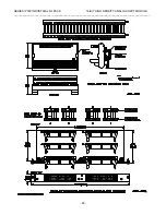
Physical Configuration..................Single Industrial I/O Pack
Module.
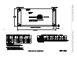
Length....................................3.880 inches (98.5 mm).
Width.....................................1.780 inches (45.2 mm).
Board Thickness....................0.062 inches (1.59 mm).
Max Component Height..........0.314 inches (7.97 mm).
Connectors:
P1 (IP Logic Interface)............50-pin female receptacle header
(AMP 173279-3 or equivalent).
P2 (Field I/O)..........................50-pin female receptacle header
(AMP 173279-3 or equivalent).
Power Requirements:
+5 Volts (
±
5%).......................30mA, Typical
40mA, Maximum.
+12 Volts (
±
5%) from P1........14mA, Typical
20mA, Maximum.
+15 Volts (
±
5%) from P2
2
-12 Volts (
±
5%) from P1........11mA, Typical
15mA, Maximum.
-15 Volts (
±
5%) from P2
2
Note:
2. The +/-12 volt power supplies are normally supplied through
P1 (logic interface connector). Optionally (jumper selectable on
the IP), the user may connect ex/-15 volt supplies through
the field I/O interface connector, P2.
Non-Isolated................................Logic and field commons have a
direct electrical connection.
ANALOG INPUTS
Input Channels (Field Access).....32 Single-ended or 16
Differential
Input Signal Type.........................Voltage (Non-isolated).
Input Ranges (DIP switch selectable):
Bipolar -5 to +5 Volts
3
Bipolar -10 to +10 Volts
3,4
Unipolar 0 to +5 Volts
3
Unipolar 0 to +10 Volts
3,4
Notes:
3. Range assumes the programmable gain is equal to one.
Additional ranges are created with other gains. Divide the
listed range by the programmable gain to determine the actual
input range. Input signal ranges may actually fall short of
reaching the specified endpoints due to hardware limitations.
For example, if an input may reach zero volts or less, a bipolar
input range should be selected.
4. These ranges can only be achieved with
±
15 Volt external
power supplies. The input ranges will be clipped if
±
12 Volt
supplies are used, typically to
±
8.5 Volt maximum inputs.
Programmable Gains....................x1, x2, x4, x8.
Input Overvoltage Protection.........VSS - 20 V to VDD + 40 V with
Power ON.
-35 V to +55 Volts Power OFF
Input Resistance...........................1000 M
Ω
, Typical.
Input Bias Current.........................1nA., Typical.
Common Mode
Rejection Ratio (60Hz)
8
.................96 dB., Typical.
Channel to Channel
Rejection Ratio (60Hz)
8
.................96 dB., Typical.
Resistance to RFI
8
........................Error is less than
±
0.25% of
FSR with field strengths up to
10V/m at frequencies of
27MHz, 151MHz,
460MHz. per SAMA PMC 33.1
test procedures
Resistance to EMI
8
.......................Error is less than
±
0.25% of
FSR under the influence of EMI
from switching solenoids,
commutator motors, and drill
motors.
(ADC) ADS7809U or AD977AR @25
°
C:
ADC.............................................Burr-Brown ADS7809U
A/D Resolution..............................16-bits.
Data Format Binary 2’s Complement and
Straight Binary
No Missing Codes
8
.......................No Missing Codes 15-bits ADC
A/D Integral Linearity Error
8
.....
±
1 LSB Typical,
±
3 LSB Maximum ADC
Unipolar Zero Error
5
.............. .
±
10mV Maximum, for 0-10V Range,
±
10mV Maximum for 0-5V Range.
Bipolar Offset Error
5
................
±
10mV Maximum, for
±
10V Range,
±
10mV Maximum for
±
5V Range.
Full Scale Error
5
......................
±
0.5
%
Maximum.
(PGA) PGA206UA @25
°
C:
PGA..............................................Burr-Brown PGA206UA
PGA Linearity Error......................
±
0.005
%
Maximum (3.27 LSB)
Offset Error RTI
5
..........................
±
1.0mV Typical,
±
2.5mV
Maximum.
Gain Error (all gains)
5
...................0. 01
%
Typical, 0. 1
%
Maximum.
Note:
5. Software calibration eliminates these error components.
Programmable Calibration Voltages
Calibration
Signal
Ideal
Value
(Volts)
Maximum
Tolerance
8
@25oC (Volts)
Maximum
Temperature
Drift
6
(ppm/oC)
Auto Zero
0.0000
±
0.000150 0
CAL0 4.9000
±
0.000228
±
6
CAL1 2.4500
±
0.000228
±
11
CAL2 1.2250
±
0.000228
±
11
CAL3 0.6125
±
0.000228
±
11
Note:
6. Worst case temperature drift is the sum of the
±
6 ppm/oC *
drift of the calibration voltage reference plus the
±
5 ppm/oC drift
of the resistors in the voltage divider.
*
±
15 ppm/
°
C for “E” Version model.

