background image

SERIES IP503 INDUSTRIAL I/O PACK                  EIA/TIA-232E & CENTRONICS COMMUNICATION MODULE
___________________________________________________________________________________________

- 4 -

This board is physically protected with
packing material and electrically
protected with an anti-static bag during
shipment.  However, it is
recommended that the board be
visually inspected for evidence of
mishandling prior to applying power

The board utilizes static-sensitive
components and should only be
handled at a static-safe workstation

CARD CAGE CONSIDERATIONS

Refer to the specifications for loading and power

requirements Be sure that the system power supplies are able to
accommodate the power requirements of the carrier board, plus
the installed IP modules, within the voltage tolerances specified

IMPORTANT: Adequate air circulation must be provided to
prevent a temperature rise above the maximum operating
temperature

The dense packing of the IP modules to the carrier board

restricts air flow within the card cage and is cause for concern
Adequate air circulation must be provided to prevent a
temperature rise above the maximum operating temperature and
to prolong the life of the electronics.  If the installation is in an
industrial environment and the board is exposed to environmental
air, careful consideration should be given to air-filtering

BOARD CONFIGURATION

Power should be removed from the board when installing IP

modules, cables, termination panels, and field wiring.  Refer to
Mechanical Assembly Drawing 4501-434 and your IP module
documentation for configuration and assembly instructions.
Model IP503 communication boards have no hardware jumpers
or switches to configure

CONNECTORS

IP Field I/O Connector (P2)

P2 provides the field I/O interface connections for mating IP

modules to the carrier boardP2 is a 50-pin female receptacle
header (AMP 173279-3 or equivalent) which mates to the male
connector of the carrier board (AMP 173280-3 or equivalent)This
provides excellent connection integrity and utilizes gold-plating in
the mating area.  Threaded metric M2 screws and spacers are
supplied with the module to provide additional stability for harsh
environments (see Mechanical Assembly Drawing 4501-434)The
field and logic side connectors are keyed to avoid incorrect
assemblyP2 pin assignments are unique to each IP model (see
Table 21) and normally correspond to the pin numbers of the field
I/O interface connector on the carrier board (you should verify this
for your carrier board)An optional interface cable (Model 5029-
944) is available to convert the field I/O connector to common
DB9 (serial port) and DB25 (parallel port) port connectors

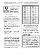
Table 21:IP503 Field I/O Pin Connections (P2)

Pin Description

Number

Pin Description

Number

COMMON

1

STB*

26

RI_A*

2

AFD*

27

DTR_A*

3

PD0

28

CTS_A*

4

ERR*

29

TXD_A

5

PD1

30

RTS_A*

6

INIT*

31

RXD_A

7

PD2

32

DSR_A*

8

SLIN*

33

DCD_A*

9

PD3

34

COMMON

10

COMMON

35

RI_B*

11

PD4

36

DTR_B*

12

COMMON

37

CTS_B*

13

PD5

38

TXD_B

14

COMMON

39

RTS_B*

15

PD6

40

RXD_B

16

COMMON

41

DSR_B*

17

PD7

42

DCD_B*

18

COMMON

43

COMMON

19

ACKN*

44

COMMON

20

COMMON

45

COMMON

21

BUSY

46

COMMON

22

COMMON

47

COMMON

23

PE

48

COMMON

24

COMMON

49

COMMON

25

SLCT

50

An Asterisk (*) is used to indicate an active-low signal

Note that the pin-wire assignments are arranged such that

IDC D-SUB ribbon cable connectors can be conveniently
attached to provide serial port A (pins 1-9), serial port B (pins 10-
18), & Centronics port (pins 26-50) connectivity (see Acromag
cable Model 5029-944)In Table 21, a suffix of “_A”, or “_B” is
appended to each pin label to denote its serial port association.
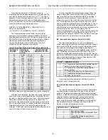
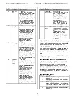
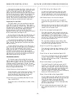
A brief description of each of the serial port signals at P2 is
included below.  A complete functional description of all P2 pin
functions (including parallel port pins) is included in Section 40
(Theory Of Operation)Be careful not to confuse the A & B port
designations of the IP module with the IP carrier board A & B slot
designations

P2 Pin Signal Descriptions

SIGNAL

DESCRIPTION

DCD_A*
DCD_B*

Data Carrier Detect - An active low signal that
indicates the carrier has been detected by the
modem.  The status of this signal is read via bit 7
of the Modem Status Register

DSR_A*
DSR_B*

Data Set Ready- A modem status signal to indicate
that it is connected to the line (it has no effect on
the transmit or receive operation)The status of this
signal is read via bit 5 of the Modem Status
Register

RxD_A
RxD_B

Receive Data Line Input - This is the receive data
input line.  During Loopback Mode, the RxD input is
disabled from the external connection and
connected to the TxD output internally

TxD_A
TxD_B

Transmit Data Line Output - This is the transmit
output data line.  In the idle state, this signal line is
held in the mark (logic 1) state.  During Loopback
Mode, the TxD output is internally connected to the
RxD input

Summary of Contents for Series IP503

Page 1: ...tion Module USER S MANUAL ACROMAG INCORPORATED 30765 South Wixom Road P O BOX 437 Wixom MI 48393 7037 U S A Tel 248 624 1541 Fax 248 624 9234 Copyright 1995 Acromag Inc Printed in the USA Data and spe...

Page 2: ...toring system This is especially important where economic property loss or human life is involved It is important that the user employ satisfactory overall system design It is agreed between the Buyer...

Page 3: ...m performance with precision analog I O applications The X suffix of the model number denotes the length in feet Model 5029 944 IP503 Serial Communication Cable A 5 foot long flat 50 pin cable with a...

Page 4: ...n assignments are unique to each IP model see Table 21 and normally correspond to the pin numbers of the field I O interface connector on the carrier board you should verify this for your carrier boar...

Page 5: ...ground to safety ground via any device connected to these ports or a ground loop will be produced and this may adversely affect operation The communication cabling of the P2 interface carries digital...

Page 6: ...ing Little Endian uses even byte addresses to store the low order byte As such use of this module on an ISAbus PC AT carrier board will require the use of the even address locations to access the 8 bi...

Page 7: ...transmitted then data is right justified to the LSB If parity is used then LCR bit 3 parity enable and LCR bit 4 type of parity are required Status for the receiver is provided via the Line Status Reg...

Page 8: ...gh to low transition start bit When the start bit is detected a counter is reset and counts the 16x sampling clock to 7 1 2 which is the center of the start bit The receiver then counts from 0 to 15 t...

Page 9: ...NOT supported by this model FIFO Control Register FCR BIT FUNCTION 0 When set to 1 this bit enables both the Tx and Rx FIFO s All bytes in both FIFO s can be cleared by resetting this bit to 0Data is...

Page 10: ...m Control Register 1 MCR Bit 4 provides a local loopback feature for diagnostic testing of the UART channel When set high the UART serial output connected to the TXD driver is set to the marking logic...

Page 11: ...d by a read of the IIR Line Status Register continued LSR Bit FUNCTION PROGRAMMING 6 Transmitter Empty TEMT 0 Not Empty 1 Transmitter Empty set when both the Transmitter Holding Register THR and the T...

Page 12: ...data lines This register is either output only or bi directional depending on the state of the extended mode bit bit 0 of the LEM register and the data direction control bit bit 5 of the LPC register...

Page 13: ...interrupt source the ACKN line of the parallel port or bit 2 of the LPS register The serial ports and the parallel port interrupts drive INTREQ0 Bit 0 of this register drives the ENIRQ line of the UA...

Page 14: ...atus of each channel can be read by the host CPU at any time during operation Two registers are used to report the status of a serial channel the Line Status Register LSR and the Modem Status Register...

Page 15: ...s the last stop bit time when the following occurs Bit 5 of the LSR THRE is 1 and there is not a minimum of two bytes at the same time in the transmit FIFO since the last time THRE 1The first transmit...

Page 16: ...Divisor Latch Access bit to permit access to the two divisor latch bytes used to set the baud rate These bytes share addresses with the Receive and Transmit buffers and the Interrupt Enable Register...

Page 17: ...puters are considered DTE devices while modems are DCE devices The EIA TIA 232E interface is the fifth revision of this standard and defines an unbalanced single ended transmission standard for unidir...

Page 18: ...ver a null modem cable connection is required to connect two like configured DTE ports due to the imbalance of drivers and receivers see Drawing 4501 572 Pins 1 18 of field I O connector P2 provide co...

Page 19: ...S INPUT BUSY Pin 11 Input Line Printer Busy Active high signal from the printer that is asserted when the printer is not ready to accept more Data The state of this bit is monitored via Bit 7 of the L...

Page 20: ...o obtain parts and repair PRELIMINARY SERVICE PROCEDURE Before beginning repair be sure that all of the procedures in Section 2 Preparation For Use have been followed Also refer to the documentation o...

Page 21: ...t maximum Choose shielded or unshielded cable according to model number The unshielded cable is recommended for digital I O while the shielded cable is recommended for optimum performance with precisi...

Page 22: ...Boards Application This panel converts the high density ribbon cable connectors coming from the APC8600 carrier board Acromag cable Model 5029 900 to screw terminals for direct wired interfaces This p...

Page 23: ......

Page 24: ......

Page 25: ......

Page 26: ......

Page 27: ......

Page 28: ......

Page 29: ......

Page 30: ......

Page 31: ......

Reviews: