background image

AR-B9673 User’s Guide


3  2  1 


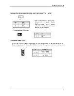
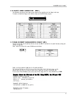
2.2 POWER ON CONNECTOR FOR ATX POWER SUPPLY    (ATX1) 


  ATX POWER BUTTON (BTON1) 


1   2 


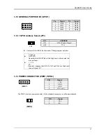
2.3 CLEAR CMOS (JP4) 


If want to clear the CMOS Setup (for example when you forgot the password, please clear the setup and then set 
the password again.), you should close the pin 2-3 about 3 seconds, then open again, set back to normal operation 
mode, close the pin 1-2.                  


PIN 

Signal 

1 PSON 

2 VCC 

3 5VSB 

Pin

Signal 

1 -PWBN 

2 GND 

JP4 

FUNCTION 

1-2 ON 

Normal Operation 

(Factory Preset) 

2-3 ON 

Clear CMOS 

* When AT power supplier is applied, jumper

2&3 should be tied together. (Factory
preset) 

* When ATX power supplier is applied,

pin1&pin 3 should be connect to proper
location of ATX power supplier. 

Summary of Contents for AR-B1673

Page 1: ...AR B9673 User s Guide 1 AR B9673 INDUSTRIAL GRADE CPU BOARD User s Guide Edition 1 1 Book Number AR B9673 07 0821...

Page 2: ...CONNECTOR PS1 PS2 10 3 6 USB PORT CONNECTOR USB1 11 3 7 IRDA INFRARED INTERFACE PORT IR1 11 3 8 FAN CONNECTOR FAN1 11 3 9 VGA CRT CONNECTOR VGA1 11 3 10 FLOPPY DRIVE CONNECTOR FDD1 12 3 11 SRAM MEMOR...

Page 3: ...his guide if you have not already installed this AR B9673 Check the packing list before you install and make sure the accessories are completely included AR B9673 CD provides the newest information re...

Page 4: ...e computer components Although areas with humid climates are much less prone to static build up it is always best to safeguard against accidents that may result in expensive repairs The following meas...

Page 5: ...ion up to True Color 32 bit 1024x768 or High Color 16 bit 1280x1024 Display Interface CRT D SUB 15 pin female connector Ultra ATA 33 66 100 IDE Interface Two PCI Enhance IDE channel The south bridge V...

Page 6: ...scribes how to install the AR B9673 At first the layout of AR B9673 is shown and the unpacking information that you should be careful is described The following lists the jumpers and switches setting...

Page 7: ...word again you should close the pin 2 3 about 3 seconds then open again set back to normal operation mode close the pin 1 2 1 3 PIN Signal 1 PSON 2 VCC 3 5VSB Pin Signal 1 PWBN 2 GND JP4 FUNCTION 1 2...

Page 8: ...ion To enable or disable the hard disk controller please use the BIOS Setup program which is explained further in chapter 5 The following table illustrates the pin assignments of the hard disk drive s...

Page 9: ...in Signal Pin Signal 1 STB 2 AFD 3 PD0 4 ERROR 5 PD1 6 INIT 7 PD2 8 SLIN 9 PD3 10 GND 11 PD4 12 GND 13 PD5 14 GND 15 PD6 16 GND 17 PD7 18 GND 19 ACK 20 GND 21 BUSY 22 GND 23 PE 24 GND 25 SLCT 26 N C 3...

Page 10: ...JST Header and 6 PIN MINI DIN keyboard mouse connector PS1 6 pin Mini DIN Keyboard Mouse Connector 1 2 3 4 5 6 Front View PS2 JST6 pin Keyboard Mouse Connector 1 6 PS2 JUMPER FUNCTION RS 232 FACTORY P...

Page 11: ...32 COM 1 will be disabled 1 5 3 8 FAN CONNECTOR FAN1 The AR B9673 provides CPU cooling Fan connector CPU connectors can supply 12V 500mA to the cooling fan 3 2 1 3 9 VGA CRT CONNECTOR VGA1 AR B9673 bu...

Page 12: ...a bank number Memory bank start from 00 last memory bank number depends on the size to the SRAM chip If on board the 512KB SRAM chip the memory bank in the range of 00 to 31 The SRAM I O Port 78H Exa...

Page 13: ...output pin are Low Level I 215 FC Generally suppose that GPIO1 s Pin1 and Pin3 are High Level then will show FC 3 13 POWER CONNECTOR PWR1 PWR2 1 4 PWR1 The PWR1 is a 4 pin power connector It s the sta...

Page 14: ...N2 8 1 PIN Signal 1 VCC 2 SBEEP 3 INTERNAL BUZZER 4 SBEEP PIN Signal 1 RST 2 GND LED INDICATION 1 GREEN HDD Active 2 RED Watch Active PIN LAN1 LAN2 1 TX TX 2 TX TX 3 RX RX 4 Not Used RX 5 RX Not Used...

Page 15: ...tchdog timer that occupies I O port 3F0 3F1 Users can use simple program to enable the watchdog timer Once you enable the watchdog timer the program should trigger it every time before it times out Wa...

Page 16: ...ogram used to initialize and set up the I O system of the computer which includes the ISA bus and connected devices such as the video display diskette drive and the keyboard The BIOS provides a menu b...

Page 17: ...ETUP The Main CMOS Setup option allows you to record some basic system hardware configuration and set the system clock and error handling If the CPU board is already installed in a working system you...

Page 18: ...up the Power On Self Test POST after the system is turned on If it is set to Enabled BIOS will skip some items Full Screen LOGO Show This itemenables you to show the company logo on the bootup screen...

Page 19: ...on is used to configure peripheral features Peripherals CMOS Setup Onboard Serial Port 1 2 These fields allow you to select the onboard serial ports addresses and IRQ Disabled 3F8 IRQ4 2F8 IRQ3 3E8 IR...

Page 20: ...P1 9 EPP1 7 On board FDD Controller This option enables the floppy drive controller on the AR B1673 On chip USB This setting is used to enable disable the onboard USB controller 5 5 PNP PCI CMOS SETUP...

Page 21: ...ards These options determine if the BIOS should remove an IRQ from the pool of availability of IRQs passed to the BIOS configurable devices If more IRQs must be removed from the pool the end user can...

Page 22: ...ot devices where AwardBIOS attempts to load the operating system The settings are Floppy Hard Disk CDROM USB FDD USB ZIP USB CDROM Disabled Boot Other Device Setting the option to Enabled allows the s...

Page 23: ...in this session Typing Y will quit the Setup utility without saving the modifications Typing N will return you to Setup utility 5 9 BIOS UPDATE The BIOS program instructions are contained within compu...

Reviews: