background image

ACROSSER  TECHNOLOGY

29

CHAPTER 4 APPLICATIONS

4.1 ANALOG INPUT CONNECTION

It is important to understand the connections between

the type of input signals, how to use them effectively, and

how to avoid ground loop. Misuse of the inputs is the most

common difficulty users experience in applying and

obtaining the best performance from data acquisition

systems. This chapter provides useful information

concerning how to connect analog signals with AR-

B3001 correctly in different types of data acquisition

applications.

The analog input connection to AR-B3001 is jumper

selectable to fit differential or single-ended analog signals.

This can be configured by inserting JP1 to right

(differential) or left (single) position. A single-ended

signal has only one signal wire for each channel. This

type of signal does not have a ground connection at the

signal source. This type of signal is also called a "floating

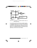
source". A standard connection of a floating signal is

shown in figure 4-1.

All manuals and user guides at all-guides.com

Summary of Contents for AR-B3001

Page 1: ...level etc The AR B3001 is constructed with a 12 bit plus polarity bit dual slop integrating A D converter It can be operated with 16 single ended or 8 differential analog inputs The analog input rang...

Page 2: ...ive half size analog input board for IBM PC XT AT and their compatibles 16 single ended or 8 differential inputs Maximum throughput 30 Hz Resolution 12 bit and a sign bit 5V to 5V input range Assembly...

Page 3: ...nd describe part number of the AR B3001 board and its accessories Part Number Description AR B3001 16 channel analog input card with user s manual AR B9006 34 pin screw terminal board for AR B3001 wit...

Page 4: ...ACROSSER TECHNOLOGY 4 This page is intentionally left blank All manuals and user guides at all guides com...

Page 5: ...of the input connector Figure 2 1 shows the location of each switch jumper and connector for AR B3001 Table 2 1 list the functions of jumper switch variable resistors and connector shown in Figure 2 1...

Page 6: ...ACROSSER TECHNOLOGY 6 Figure 2 1 Board Layout of AR B3001 All manuals and user guides at all guides com...

Page 7: ...e address switch DIP SW The AR B3001 is factory configured for a base address of 3e0 Hex If this base address is already occupied you will need to change the base address switch setting It is essentia...

Page 8: ...64 Switch 6 A7 80 128 Switch 7 A8 100 256 Switch 8 A9 200 512 Address 200 A9 100 A8 80 A7 40 A6 20 A5 10 A4 8 A3 4 A2 Hex or Address 512 A9 256 A8 128 A7 64 A6 32 A5 16 A4 8 A3 4 A2 Dec A9 A2 0 If swi...

Page 9: ...2E8 2EF Serial Port 4 COM4 2F8 2FF Serial Port 2 COM2 300 31F Prototype Card Streaming Type Adapter 378 37F Parallel Printer Port 2 LTP 2 380 38F SDLC Bisynchronous 2 3A0 3AF Bisynchronous 1 3B0 3BF...

Page 10: ...are to be used To select eight differential input channels move the jumpers to the right side Likewise to select 16 single ended analog input channels move the jumpers to the left side as shows in Fi...

Page 11: ...igured as single ended input Pin Descriptions Pin Descriptions 1 CH 0 2 AGND 5 CH 1 6 AGND 9 CH 2 10 AGND 13 CH 3 14 AGND 17 CH 4 18 AGND 21 CH 5 22 AGND 25 CH 6 26 AGND 29 CH 7 30 AGND 3 CH 8 4 AGND...

Page 12: ...4 21 CH 5 23 CH 5 25 CH 6 27 CH 6 29 CH 7 31 CH 7 Table 2 4 Input Connector Differential 2 2 Hardware Installation This section provides general instructions for installing the AR B3001 card For more...

Page 13: ...ssary 5 Choose an available option slot Remove the screw that secures the expansion slot cover to the system unit 6 Hold the AR B3001 in one hand With the other hand touch any metallic part of the com...

Page 14: ...ACROSSER TECHNOLOGY 14 This page is intentionally left blank All manuals and user guides at all guides com...

Page 15: ...utomaticallyfallonafour byteboundary Theseregisters of the AR B3001 are located as follows Address Read Function Write Function Base 0 EOC Status N A Base 1 Converted Data Control Register Base 2 Not...

Page 16: ...0 means the A D converter is in the auto zero configurationandisreadyforthenextconversion The A D data registers contain valid data of previous conversions EOC 1 means the A D converter is busy and t...

Page 17: ...lestheA Dconverter output the low byte of converted data DL 1 enables the A D converter to output the low byte data DL 0 disables the A D converter to output the low byte data Note that DH and DL can...

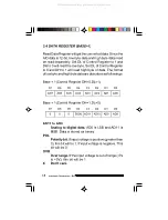
Page 18: ...aredescribesasfollowings Base 1 Control Register DH 0 DL 1 D7 D6 D5 D4 D3 D2 D1 D0 AD7 AD6 AD5 AD4 AD3 AD2 AD1 AD0 Base 1 Control Register DH 1 DL 0 D7 D6 D5 D4 D3 D2 D1 D0 0 0 0 SIGN AD11 AD10 AD9 AD...

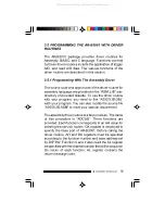
Page 19: ...your program you need to link A3001LIB OBJ wiith your program You can also modify the source file A3001LIB ASM to meet your special requirement The assembly driver routine is a far procedure The name...

Page 20: ...channel and sends a pulse to trigger the ADC Input Arguments The following input arguments have to be initialized before calling the function AH 0 specifies function 0 AL Channel number Valid number...

Page 21: ...ately after trigger ADC Function1needtobecalledtocheckendofconversion and read converted data To perform trigger and return with converted data use function 2 Example MOV AH 0 Specify function 0 MOV D...

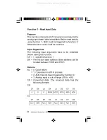
Page 22: ...to be initialized before calling the function AH 1 specifies function 1 DX The I O port base address Base address can be located between 100H and 3FCH Returns AL 0 Good return 1 Conversion is still i...

Page 23: ...ored as 12 bit binary and ranges between 000H and FFFH Programming Note 1 Function 0 should be called prier to read input data by using function 1 2 Base address specified must match the setting of DI...

Page 24: ...AL Channel number Valid number is 0 to 7 for differential input or 0 to 15 for single ended input DX The I O port base address Base address can be located between 100H and 3FCH Returns AL 0 Good retu...

Page 25: ...below 0 volt AD0 to AD11 Analog data AD0 is LSB and AD11 is MSB Data is stored as 12 bit binary and ranges between 000H and FFFH Example MOV AH 2 Specify function 2 MOV DX 3E0H Base address CALL ADCL...

Page 26: ...ables BASEPORT The base port address of AR B3001 I O port It can be located in the range of H100 to H3FC ADCHN The channel number of the input channel for which analog input is going to be acquired Re...

Page 27: ...utp The C driver routine is saved as the file name of C3001lib C in the C_LIB sub directory The syntax of this routine is described as bellow int c3001lib int port int channel Where int port Base port...

Page 28: ...ACROSSER TECHNOLOGY 28 This page is intentionally left blank All manuals and user guides at all guides com...

Page 29: ...ow to connect analog signals with AR B3001 correctly in different types of data acquisition applications The analog input connection to AR B3001 is jumper selectabletofitdifferentialorsingle endedanal...

Page 30: ...annel and responds only to difference between high and low inputs The signal source ground and the AR B3001 ground will not be at exactly the same voltage since they are connected through the ground r...

Page 31: ...o differential input To avoid the ground loop noise and unreliable readings the signal ground should be connected to the LOW input of AR B3001 differential input If the ground referred signal source i...

Page 32: ...t configuration should be used Toconnectafloatingsignalsourcetothedifferential input connecting a jumper wire between negative and analog ground of AR B3001 effectively turns the differential input in...

Page 33: ...oning components For example the user can easily implement low pass filter voltage attenuator and currentshuntfunctionsbyaddingresistorsandcapacitors on the reserved circuit pads A 60 cm flat ribbon c...

Page 34: ...ifferential input Attenuation R3 R1 R2 R3 C1 not installed C Low pass filter for single ended input freq 3dB 1 2 R1 C1 R2 0 R3 not installed D 4 20 mA current to voltage converter R3 250 0 1 precision...

Page 35: ...ssembly language driver routine A3001LIB ASM BAS_LIB BASIC driver routine B3001LIB BAS and demo program B3001DM BAS C_LIB C language driver routine C3001LIB C and demo program C3001DM C 5 1 DEMO PROGR...

Page 36: ...tines serve important functions and are provided to make your application programming easier Instead of coding these routines yourself you need only to call them into your program at the points needed...

Page 37: ...ssist your calibration work This program shows the input voltage for each A D input and help you to calibrate the AR B3001 card In addition to the calibration program a 4 1 2 digit digital multimeter...

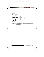
Page 38: ...equal to 1 3 Apply an analog input of 2 5V and adjust the full scale pot VR1 and VR2 for a reading of 2 5V Other inputs such as 1 25V and 3 75V can be applied to check the linearity 4 If differential...

Page 39: ...ACROSSER TECHNOLOGY 39 G Voltage Calibrator Ground AR B3001 Figure 6 1 Connection of Common Mode Rejection Adjustment All manuals and user guides at all guides com...

Page 40: ...Sampling Rate 30 times per second Linearity 1 bit Temp Coef 1 ppm C typ 5 ppm C max CMRR 50 uV V Noise 15 uV p p typ A D Converter ICL7109 Input Impedance 1M ohms Software Driver Assembly BASICA and...

Page 41: ...ACROSSER TECHNOLOGY 41 All manuals and user guides at all guides com...

Reviews: