background image

PA 358 

Technical description    Chapter 4 

4 TECHNICAL 

DATA 

4.1 Electromagnetic 

compatibility 

The board has been subjected to EMC tests in an accredited laboratory in 
accordance with the norms EN50082-2, EN55011, EN55022. 
The board complies as follows with the limit values set by the norm EN50082-2:  
 True 

value Set value 

ESD ............................................................................  4 kV 

4 kV 

Fields..........................................................................  10 V/m 

10 V/m 

Burst ...........................................................................  4 kV 

2 kV 

Conducted radio interferences ...................................  10 V 

10 V 

Noise emissions  ........................................................   B-class 


WARNING! 

The EMC tests have been carried out in a specific appliance 
configuration. We guarantee these limit values 

only 

in this 

configuration

1)

 .  

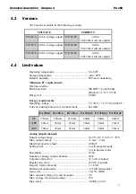
4.2 

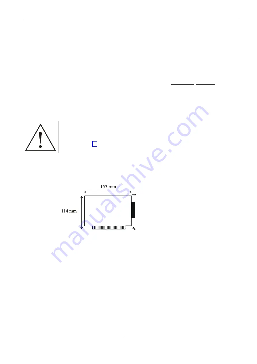
Physical set-up of the board 

The board is assembled on a 4-layer printed circuit card. 


Weight: 150 

Installation in: 

XT / AT slot 

Connection to the peripheral through 37-pin SUB-D male connector 
Standard cables: 

ST010 or ST011 

Screw terminal boards: 

PX 901-AG, PX 901-A for 

voltage

 outputs 

 (PA 

358-4/-6/-8) 

 PX 

901-ZG 

for 

current

 outputs 

 (PA 

358-4C/-6C/-8C) 


1) We transmit our appliance configuration on request. 

Summary of Contents for ADDIALOG PA 358

Page 1: ...Technical support 49 0 7223 9493 0 Technical description ADDIALOG PA 358 Analog output board 10th edition 06 2001 ...

Page 2: ...ntrusion of foreign bodies and by influence beyond the user s control Licence for ADDI DATA software products Read carefully this licence before using the software ADDISET and ADDIMON The right for using this software is given to the customer if he she agrees to the conditions of this licence this software can only be used for configuring ADDI DATA boards copying the software is forbidden except f...

Page 3: ...this leaflet is not with the manual please contact us and ask for it Observe the instructions of the manual Make sure that you do not forget or skip any step We are not liable for damages resulting from a wrong use of the board Symbols used It designates a possibly dangerous situation If the instructions are ignored the board PC and or peripheral may be damaged IMPORTANT designates hints and other...

Page 4: ... the form TD358 020 Following norms have been applied to test the product regarding electromagnetic compatibility l l l l EN55011 03 91 l l l l EN55022 08 94 l l l l EN50082 2 03 95 We point out that l the conformity and herewith the permission of use expire if the user alters the product without consulting with the manufacturer l non skilled users are to have the operational area of the product a...

Page 5: ...ss through DIP switches 12 6 2 Inserting the board 13 6 2 1 Opening the PC 13 6 2 2 Plugging the board into the slot 14 6 2 3 Closing the PC 14 6 3 Installing the software 15 6 3 1 Software installation under MS DOS and Windows 3 11 15 6 3 2 Software installation under Windows NT 9x 15 6 4 Board configuration with ADDIREG 16 6 4 1 ADDIREG installation 16 6 4 2 Program description 17 6 4 3 Register...

Page 6: ...Adjustment of the current output channels 30 8 5 1 0 20 mA adjustment Example for channel 0 31 8 5 2 4 20 mA adjustment Example for channel 0 31 8 5 3 Measuring the current 31 8 6 Operating the board 32 9 DEVICE DRIVER 35 9 1 Introduction 35 9 2 Software functions API 37 9 2 1 Base address 37 1 i_PA358_SetBoardInformation 37 2 i_PA358_CloseBoardHandle 37 9 2 2 Analog output channels 38 1 i_PA358_W...

Page 7: ...crew terminal board PX 901 and cable ST010 23 Fig 7 3 Connection of the voltage output channels 24 Fig 7 4 Connection of the current output channels Floating load 24 Fig 7 5 Connection of the current output channels Floating supply 24 Fig 8 1 Setup Channel 0 and 1 25 Fig 8 2 Schematic diagram of the watchdog circuitry 28 Fig 8 3 Measuring the current 31 Fig 8 4 Description of the task 32 Fig 8 5 C...

Page 8: ... and immunity Increased noise emission or decreased noise immunity could result in the system not being conform anymore Check the shielding capacity of the PC and cable prior to putting the device into operation The connection with our standard cable ST010 complies with the specifications metallized plastic hoods shielded cable cable shield folded back and firmly screwed to the connector housing T...

Page 9: ...ersons trained in electronics are entitled to perform the following works installation use maintenance 2 2 Personal protection Consider the country specific regulations about the prevention of accidents electrical and mechanical installations radio interference suppression ...

Page 10: ...Technical description Chapter 3 PA 358 3 3 HANDLING THE BOARD Fig 3 1 Wrong handling Fig 3 2 Correct handling ...

Page 11: ...terferences 10 V 10 V Noise emissions B class WARNING The EMC tests have been carried out in a specific appliance configuration We guarantee these limit values only in this configuration1 4 2 Physical set up of the board The board is assembled on a 4 layer printed circuit card Weight 150 g Installation in XT AT slot Connection to the peripheral through 37 pin SUB D male connector Standard cables S...

Page 12: ...y requirements Operating voltage 5 V 5 12 V from the PC Current consumption im mA without load See table PA 358 8 PA 358 6 PA 358 4 PA 358 8C PA 358 6C PA 358 4C 5V 230mA 220mA 210mA 60mA 60mA 60mA 12V 50mA 38mA 26mA 50mA 38mA 26mA 12V 50mA 38mA 26mA 50mA 38mA 26mA Analog output channels Output voltage range 0 10 V 0 5 V 10 V 5 V Max output current 5 mA 5 mA Maximal capacitive load 1000 pF Settlin...

Page 13: ...PA 358 Technical description Chapter 5 6 5 SETTINGS 5 1 Component scheme Fig 5 1 Component scheme ...

Page 14: ...Technical description Chapter 5 PA 358 7 5 2 Jumper location and settings at delivery Fig 5 2 Jumper location and settings at delivery ...

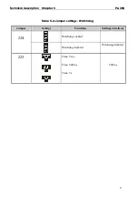
Page 15: ...ons in fig 5 2 The watchdog function is valid for all channels Table 5 1 Jumper settings Channel 0 Jumper Settings Functions Settings at delivery J1 Set Value of the DAC I after reset Unipolar zero Unipolar zero Not set Value of the DAC I after reset Bipolar zero J2 Output range for channel 0 Bipolar Output range for channel 0 Unipolar Unipolar J4 Output range for channel 0 0 10 V 0 10 V Output ra...

Page 16: ...description Chapter 5 PA 358 9 Table 5 2 Jumper settings Watchdog Jumper Settings Functions Settings at delivery J24 Watchdog enabled Watchdog disabled Watchdog disabled J23 Time 5 ms Time 500 ms Time 5 s 500 ms ...

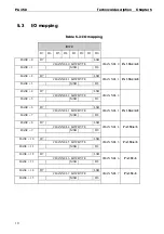
Page 17: ...PA 358 4 6 8 BASE 3 MSB D8 BASE 4 D7 LSB CHANNEL 2 LOWBYTE CHANNEL 2 BASE 5 MSB D8 BASE 6 D7 LSB CHANNEL 3 LOWBYTE CHANNEL 3 PA 358 4 6 8 BASE 7 MSB D8 BASE 8 D7 LSB CHANNEL 4 LOWBYTE CHANNEL 4 PA 358 6 8 BASE 9 MSB D8 BASE 10 D7 LSB CHANNEL 5 LOWBYTE CHANNEL 5 PA 358 6 8 BASE 11 MSB D8 BASE 12 D7 LSB CHANNEL 6 LOWBYTE CHANNEL 6 PA 358 8 BASE 13 MSB D8 BASE 14 D7 LSB CHANNEL 7 LOWBYTE CHANNEL 7 PA...

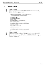
Page 18: ... Switch off the PC 2 Install the first board 3 Start the PC 4 Install ADDIREG once is enough 5 Configure the board 6 Install the driver and the samples if necessary 7 Switch off the PC 8 Install the second board 9 Start the PC 10 Configure the board 11 Install the driver and the samples if necessary etc IMPORTANT To install the new version of ADDIREG please uninstall first the current version from...

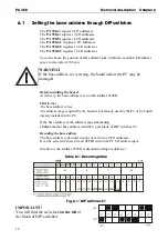
Page 19: ... damaged Before installing the board At delivery the base address is set on the address 0390H Check that the base address is free the address range required by the board is not already used by the PC or by boards already installed in the PC If the base address or the address range are wrong Select another base address with the 8 pole block of DIP switches S1 Decoding the base address The base addr...

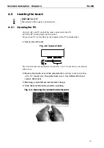
Page 20: ...manual of the PC manufacturer 1 Select a free ISA slot Fig 6 2 types of slots The board can be inserted either in a slot XT or AT It can also be inserted in EISA slots 2 Remove the back cover of the selected slot according to the instructions of the PC manufacturer Keep the back cover You will need it if you remove the board 3 Discharge yourself from electrostatic charges 4 Take the board from its...

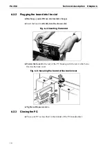
Page 21: ...Insert the board vertically into the chosen slot Fig 6 4 Inserting the board Fasten the board to the rear of the PC housing with the screw which was fixed on the back cover Fig 6 5 Securing the board at the back cover Tigthen all loosen screws 6 2 3 Closing the PC Close your PC as described in the manual of the PC manufacturer ...

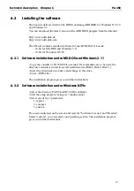
Page 22: ...opy the contents of PA358 16bit on a disk If several disks are to be used the directory contents is stored in several subdirectories Disk1 Disk2 Disk3 Insert the first disk into a drive and change to this drive Enter INSTALL The installation program gives you further instructions 6 3 2 Software installation under Windows NT 9x Select the directory PA358 winNT 9x Driver Disk1 Start the setup progra...

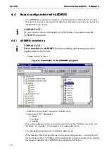
Page 23: ...and starting any other application for the board Change to the CD drive Fig 6 6 Installation of the ADDIREG program Start the set up program setup exe double click Select one of the 3 parameters 1 typical 2 compact 3 custom Proceed as indicated on the screen and read attentively the Software License and Readme In custom you can select your operating system The installation program gives you furthe...

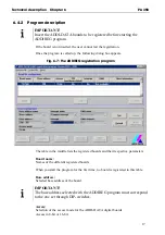
Page 24: ...ADDIREG registration program The table in the middle lists the registered boards and their respective parameters Board name Names of the different registered boards When you start the program for the first time no board is registered in this table Base address Selected base address of the board IMPORTANT The base address selected with the ADDIREG program must correspond to the one set through DIP ...

Page 25: ...h the pull down menu The corresponding address range is displayed in the field below Base address Base address In this box you can select the base addresses of your PC board The free base addresses are listed The used base addresses do not appear in this box Interrupt name Description of the used IRQ lines for the board Select a name though the pull down menu The corresponding interrupt line is di...

Page 26: ...stration of a board Select the board to be deleted and click on Clear Set Sets the parameterized board configuration The configuration should be set before you save it Cancel Reactivates the former parameters of the saved configuration Default Sets the standard parameters of the board More information You can change the board specific parameters like the identifier string the COM number the operat...

Page 27: ...he wished board Click on OK The default address interrupt and the other parameters are automatically set in the lower fields The parameters are listed in the lower fields If the parameters are not automatically set by the BIOS you can change them Click on the wished scroll function s and choose a new value Activate your selection with a click Once the wished configuration is set click on Set Save ...

Page 28: ... click on Set Save the configuration with Save You can test if the registration is OK This test controls if the registration is right and if the board is present If the test has been successfully completed you can quit the ADDIREG program The board is initialised with the set parameters and can now be operated In case the registration data is to be modified it is necessary to boot your PC again A ...

Page 29: ...e complete removal of the program Uninstall ADDIREG Click on Deinstall registration for AddiReg Proceed as indicated until the complete removal of ADDIREG You can also download the ADDI UNINSTALL program from the Internet 6 6 Software downloads from the Internet You can download the latest version of the device driver for the PA 358 board http www addi data de or http www addi data com If you have...

Page 30: ...cal description Chapter 7 PA 358 23 7 CONNECTION TO THE PERIPHERAL 7 1 Connector pin assignment Fig 7 1 37 pin SUB D male connector 7 2 Connection examples Fig 7 2 Screw terminal board PX 901 and cable ST010 ...

Page 31: ...hnical description Chapter 7 24 Fig 7 3 Connection of the voltage output channels Fig 7 4 Connection of the current output channels Floating load Fig 7 5 Connection of the current output channels Floating supply ...

Page 32: ... via a latch signal 12 bit latch register This occurs through a dummy I O read on the base address This unit also has an asynchronous clear input with sets both channels to unipolar zero or bipolar zero The value of the output channels is defined after power on reset This input is also used to reset the output channels after watchdog time has run down Should the board no longer be accessed by soft...

Page 33: ...he lowbyte When the analog output value has to be changed then the new digital value has to be changed in both addresses The value is then written on the base address with a dummy I O read command in the DAC register 1st example the value 2048 decimal should be written out on channel 0 Program SET_DAC_OUTPUT Const Base 390 Base address of PA 358 Var Dummy Byte Value Word Begin Value 2048 Portw Bas...

Page 34: ...o 07FF Hex 1 2 Full Scale 1LSB Zero 1LSB 0000 Hex Zero Full Scale USB Unipolar Straight Binary BOB Bipolar Offset Binary Example Channel 0 set on written with value then the output has the following state 0 5V 0000 Hex 0V 0 5V 0FFF Hex 5V 0 5V 0800 Hex 2 5V 4 20mA 0000 Hex 4mA 4 20mA 0FFF Hex 20mA 4 20mA 0800 Hex 12mA 10V 0000 Hex 10V 10V 0FFF Hex 10V 10V 0800 Hex 0V ...

Page 35: ...i e no new value is written on one of them then all outputs are reset depending on the adjustment J1 J6 J11 J16 to Unipolar zero or Bipolar zero One jumper adjusts two output channels Depending on the jumper adjustment If the jumper is set then the corresponding unit is loaded after reset with 0000Hex Unipolar zero Example If the range 10 V is selected then the output voltage obtained after reset ...

Page 36: ... channels 0 1 J6 DAC II channels 2 3 J11 DAC III channels 4 5 J16 DAC IV channels 6 7 a If J1 J6 J11 and or J16 are plugged 0 then the DAC registers are loaded with value 0000Hex as soon as the clear input is activated A clear is generated by a system reset at initialisation or after the watchdog time if set has run down The outputs are set to following output values after a reset in unipolar mode...

Page 37: ... 5 Adjustment of the current output channels If you use the current outputs you can adjust them To this purpose each output has been equipped with two potentiometers One for the GAIN adjustment at 0 20 mA 4 20 mA One for the OFFSET adjustment at 4 mA Table 8 2 Potentiometers for adjusting the current output channels Channel Offset Gain 0 P1 P2 1 P3 P4 2 P5 P6 3 P7 P8 4 P9 P10 5 P11 P12 6 P13 P14 7...

Page 38: ... adjustment Example for channel 0 All channels are identically set up Jumper J25 is not set and J26 is set J41 is set on 4 20mA mode Write the value 000Hex on channel 0 There must be a current of 4 mA Otherwise please calibrate on 4 mA with potentiometer P1 Write the value FFFHex on channel 0 There must be a current between 19 99 and 20 00 mA Otherwise please calibrate in this range with adjusting...

Page 39: ...d and positioned per PC Fig 8 4 Description of the task The PID controllers are analog controllers The predetermined value is set via a 4 20mA current loop it is possible to read it back The actual value is connected to the PID controllers with a 4 20mA current loop it is also to be supervised and recorded in order to obtain a daily production report Alarms can also be set via PC so that an electr...

Page 40: ...th 8 free addresses in the PC Selection address 0300Hex Supervision per watchdog is necessary The critical time for the process is in seconds A time of 5s is selected through J23 The watchdog is enabled through J24 Reset after the watchdog time has run down or after Power On Reset the current loops are to be set at 4 mA Unipolar zero Channels 0 to 3 are to be operated in 4 20 mA mode Thus the foll...

Page 41: ...PA 358 Technical description Chapter 8 34 Fig 8 6 Jumper settings for channel 1 0 in 4 20 mA ...

Page 42: ...Borland Pascal Microsoft Visual Basic Dos Microsoft Visual Basic Windows VOID void void pointer any BYTE unsigned char unsigned char byte integer integer INT int int integer integer integer UINT unsigned int unsigned int word long long LONG long long longint long long PBYTE unsigned char unsigned char var byte integer integer PINT int int var integer integer integer PUINT unsigned int unsigned int...

Page 43: ...ID void void pointer any BYTE unsigned char unsigned char byte integer integer INT int int integer integer integer UINT unsigned int unsigned int long long long LONG long long longint long long PBYTE unsigned char unsigned char var byte integer integer PINT int int var integer integer integer PUINT unsigned int unsigned int var long long long PCHAR char char var string string string ...

Page 44: ...utput channels A handle is returned to the user which allows to use the next functions Handles allow to operate several boards Return value 0 No error 1 Base address already used 2 Number of analog output channels is wrong 3 No handle is available for the board up to 10 handles can be used 2 i_PA358_CloseBoardHandle IMPORTANT Call up this function each time when you want to leave the user program ...

Page 45: ...parameter of the board is wrong 2 The channel number is wrong 3 The output value is too high 2 i_PA358_WriteSevAnalogOutput Syntax Return value i_PA358_WriteMoreAnalogValue BYTE b_BoardHandle BYTE b_FirstChannelNbr BYTE b_NbrOfChannel PUINT pui_ValueArray Parameter BYTE b_BoardHandle Handle of board PA 358 BYTE b_FirstChannelNbr Number of the first channel 1 to 8 BYTE b_NbrOfChannel Number of chan...

Page 46: ...ue 0 is written in the buffer of channel 2 The value 2048 is written in the buffer of channel 3 The value 4095 is written in the buffer of channel 4 Return value 0 No error 1 The handle parameter of the board is wrong 2 The channel number is wrong 3 Output value s too high 4 The number of channels you wish to write on is wrong See function i_PA358_SetBoardInformation ...

Page 47: ... 30 Measuring the current 31 Setup 25 Component scheme 6 Connection to the peripheral Connector pin assignment 23 Principle 23 Device driver 35 39 DIP switches 12 Electromagnetic compatibility 4 EMC See Electromagnetic compatibility Functions 25 34 I O mapping 10 Installation 11 12 Internet error analysis 22 Jumper Location 7 Settings at delivery 7 Limit values 5 Reset 28 Unipolar bipolar 29 User ...

Reviews: