


Technical description Chapter 4
PA 358
5
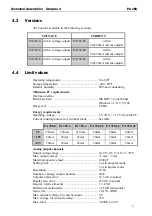
4.3 Versions
The board is available in the following versions
VOLTAGE CURRENT
PA358-4 with 4 voltage outputs PA358-4C
with 4
0(4)-20mA current outputs
PA358-6 with 6 voltage outputs PA358-6C
with 6
0(4)-20mA current outputs
PA358-8 with 8 voltage outputs PA358-8C
with 8
0(4)-20mA current outputs
4.4 Limit
values
Operating temperature: .............................................. 0 to 60
°
C
Storage temperature: .................................................. -20 to 80
°
C
Relative humidity: ..................................................... 80% non condensing
Minimum PC requirements:
ISA bus interface
Betriebssystem: .......................................................... MS DOS 3.3 oder höher
Windows 3.1, NT, 95, 98
Bus speed: .................................................................. 8 MHz
Energy requirements:
Operating voltage: ..................................................... 5 V
±
5% / ± 12 V from the PC
Current consumption im mA (without load): ............ See table
PA 358-8 PA 358-6 PA 358-4 PA 358-8C PA 358-6C PA 358-4C
5V
230mA 220mA 210mA 60mA 60mA 60mA
+12V
50mA 38mA 26mA 50mA 38mA 26mA
-12V
50mA 38mA 26mA 50mA 38mA 26mA
Analog output channels
Output voltage range: ................................................. 0-10 V; 0-5 V;
±
10 V,
±
5 V
Max. output current: ................................................... +5 mA / -5 mA
Maximal capacitive load: ........................................... 1000 pF
Settling time: .............................................................. 4 µs in unipolar mode
5 µs in bipolar mode
Resolution: ................................................................. 12-bit
Number of analog output channels: ........................... 4/6/8
Unipolar offset error: ................................................. +0,5 mV maximal
Bipolar zero error: ...................................................... ±10 mV maximal
Integral, relative linearity: ......................................... ± ½ LSB
Differential nonlinearity: ........................................... ± 1 LSB (monotonic)
Gain error: .................................................................. ± 0,15% (FSR)
Max. residual voltage for current output: .................. 6 V
Max. voltage for current feeding: .............................. 35 V
Max. load: ..................................................................
<
800 R at 24 V