background image


Mechanical Layout 

F

G

H

I

J

K

A

B

C

D

E

L

M

N

O

P

Q

R

S

W

X

Y

Z

b

a

c

d

T

U

V

e

f

g

F

G

H

I

J

K

A

B

C

D

E

L

M

N

O

P

Q

R

S

W

X

Y

Z

b

a

c

d

T

U

V

e

f

g


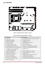
Figure 3: Onboard Connector Locations- Top Side 


Table 2: Onboard Connector Definitions - Top Side  

Item  Description 

Item

Description 

CPU socket    

Panel backlight power and resolution jumper (CN13) 

DRAM socket for DIMM1 

MXM connector (CN5) 

DRAM socket for DIMM2 

PCB edge connector 

CPU Fan connector  

RTC battery connector (CN16) 

System fan connector  

GPU fan connector  

2x USB2.0 pin header (CN22) 

12V DC in connector (CN3) 

RS-232 pin header for COM1 (CN7) 

Display port C and Display port D from MXM  

RS-232/422/485 pin header for COM2 (CN8) 

Display port A and Display port B from MXM  

2x USB 3.2 Gen1 x1 pin headers (Q370) 
2x USB 2.0 pin headers (H310) 

HDMI from CPU   

Multi-purpose connector (CN6) 

LAN1 and USB 3.2 Gen1 x1 ports 1/2  

Audio pin header (CN9) 

LAN4 and USB 3.2 Gen1 x1 ports 3/4  

PCIe power connector (CN10) 

LAN2 and LAN3   

SATA connector (SATA1) 

Display port 1 and Display port 2 from CPU  

SATA connector (SATA2) 

BMC status LED (LED2, Blue) 

SATA power connector (CN14) 

BMC watchdog LED (LED3, Red) 

Power on module connector (CN12) 

Data format and Color Depth selection for LVDS (SW1) 

DIO connector (CN11) 


Summary of Contents for AMSTX-CF Series

Page 1: ...UTING AMSTX CF Series User s Manual Embedded Motherboard supporting MXM Graphics Module with 8th 9th Generation Intel Core i7 i5 i3 in LGA1151 Socket Manual Rev 1 1 Revision Date April 20 2021 Part Number 50M 00020 1010 ...

Page 2: ...nic Equipment WEEE directive Environmental protection is a top priority for ADLINK We have enforced measures to ensure that our products manufacturing processes components and raw materials have as little impact on the environment as possible When products are at their end of life our customers are encouraged to dispose of them in accordance with the product disposal and or recovery programs presc...

Page 3: ...on Date By 1 0 Initial release 2020 12 21 JC 1 1 Add new models EGX MXM RTX3000 and EGX MXM RTX5000 add MXM cooler for RTX5000 and 500W power supply update specifications update block diagrams add mating connector list update DisplayPort BIOS settings 2021 04 20 JC ...

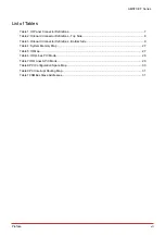
Page 4: ...mperatures 4 2 7 Humidity 4 2 8 Certificate EMC 5 2 9 Form Factor 5 2 10 Operating Systems 5 2 11 Functional Block Diagram 5 3 Mechanical Layout 7 3 1 Connector Locations 7 3 2 Mechanical Dimensions 10 4 Connector Pinouts 11 4 1 LEDs 11 4 2 Internal Connectors 12 4 3 Jumper and Switch Settings 21 5 Driver Installation 25 6 System Resources 27 6 1 System Memory Map 27 6 2 I O Map 27 6 3 Interrupt R...

Page 5: ...h Windows API 33 8 DisplayPort BIOS Settings 35 8 1 MXM P1000 P2000 T1000 RTX3000 RTX5000 35 8 2 MXM P3000 P5000 35 9 BIOS Setup 37 9 1 Menu Structure 38 9 2 Main 39 9 3 Advanced 42 9 4 Chipset 56 9 5 Security 61 9 6 Boot 62 9 7 Save Exit 63 Safety Instructions 64 Getting Service 65 ...

Page 6: ...gures Figure 1 Functional Block Diagram 5 Figure 2 IO Panel Connector Locations 7 Figure 3 Onboard Connector Locations Top Side 8 Figure 4 Onboard Connector Locations Bottom Side 9 Figure 5 Mechanical Dimensions Top View 10 ...

Page 7: ...Connector Definitions Top Side 8 Table 3 Onboard Connector Definitions Bottom Side 9 Table 4 System Memory Map 27 Table 5 IO Map 27 Table 6 IRQ Lines PIC Mode 28 Table 7 IRQ Lines APIC Mode 28 Table 8 PCI Configuration Space Map 30 Table 9 PCI Interrupt Routing Map 31 Table 10 SMBus Slave Addresses 31 ...

Page 8: ...viii Preface This page intentionally left blank ...

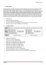
Page 9: ...delivering high performance long life embedded graphics solutions for a variety of market segments 1 1 Packing List AMSTX CF embedded motherboard CPU cooler bracket P N 32 50015 0100 A0 M3 screw P head L4 Ni for M 2 E B M Key P N 33 03013 0040 3 for Q370 2 for H310 2x M3 screw I head L4 Nylok for MXM P N 33 03306 0040 1 2 Available Models Model AMSTX CFP12 Q370 AMSTX CFP35 Q370 AMSTX CFP12 H310 AM...

Page 10: ...2 Introduction This page intentionally left blank ...
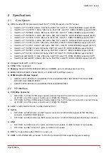
Page 11: ...M Cache 35W TDP LGA1151 DDR4 2400MHz support 2C 2T z Chipset Intel Q370 or H310 Chipset z TPM TPM 2 0 optional z Memory Non ECC DDR4 2666 2400 MHz 2x SODIMM up to 64 GB dependent on CPU z BIOS AMI UEFI BIOS 256 Mb Q370 or 128 Mb H310 SPI flash memory z MXM Graphics Module Support AMSTX CFP12 Q370 H310 EGX MXM P1000 EGX MXM P2000 EGX MXM T1000 EGX MXM RTX3000 EGX MXM RTX5000 AMSTX CFP35 Q370 H310 E...

Page 12: ...S optional default is WO LVDS dual channel 24 bit or 18 bit up to 1920 x 1200 Hz From MXM 4x DP connectors signal from MXM module resolution based on MXM module DP support 2 4 Audio z Audio Codec Realtek ALC262 VC2 GR or ALC888S VD2 GR Interfaces Default 1x 10 pin wafer box header for Mic in Line out Line in connector via additional audio module Optional 1 Mic in 6W speaker_out_L 6W speaker_out_R ...

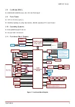
Page 13: ...ort A Port B Port C Port D DP CN DP CN HDMI CN AMP TPA3132D2_TI DMI USB3 Gen1x1 4 RJ45 x1 CN 2 2 2 2 USB3 Gen1x1 USB2 0 LAN HDA Line In Mic In Line Out USB2 0 Speaker Out USB3 Gen1x1 PCIex1 USB2 0 PCIex1 SATA USB2 0 PCIex1 2 USB2 0 ADM213EA_ADI UART UART System FAN GPU FAN BIOS SPI PCIex4 or SATA USB3 Gen1x1 2 USB3 Gen1x1 2 TPM 2 0 SLB9665_Infineon 2 H31 0 2 Q370 USB2 0 For Q370 SKU 1x PCIe x8 PCB...

Page 14: ...6 Specifications This page intentionally left blank ...

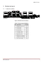
Page 15: ...able 1 IO Panel Connector Definitions Item Description Remarks A DisplayPort from CPU CN1 B LAN I210 AT RJ453 C LAN I210 AT CN24 D LAN I219 LM CN23 E 2x USB 3 2 Gen1 x1 CN24 F 2x USB 3 2 Gen1 x1 CN23 G HDMI from CPU HDMI1 H DisplayPort from MXM U13 I DisplayPort from MXM U27 J 12V DC in connector CN3 E F A B H I C D G J ...

Page 16: ...in header CN22 W 12V DC in connector CN3 G RS 232 pin header for COM1 CN7 X Display port C and Display port D from MXM H RS 232 422 485 pin header for COM2 CN8 Y Display port A and Display port B from MXM I 2x USB 3 2 Gen1 x1 pin headers Q370 2x USB 2 0 pin headers H310 Z HDMI from CPU J Multi purpose connector CN6 a LAN1 and USB 3 2 Gen1 x1 ports 1 2 K Audio pin header CN9 b LAN4 and USB 3 2 Gen1...

Page 17: ...nboard Connector Definitions Bottom Side Item Description A DB40 connector CN19 B M 2_B Key connector CN17 C M 2_M Key connector CN20 D M 2_E Key connector CN15 E LVDS CN21 F Multi IO voltage selection SW9 G RI 5V 12V selection SW7 H HSIO Selection SW5 I LVDS Channel selection SW2 J DIO voltage selection SW8 K LVDS VDD selection SW6 K ...

Page 18: ...t 3 2 Mechanical Dimensions Dimensions mm Top View 23 50 162 32 5 162 32 169 80 5 132 35 167 32 183 72 197 72 7 60 4 12 90 34 93 55 92 77 62 116 87 147 86 Figure 5 Mechanical Dimensions Top View Side View 31 05 1 60 8 50 ...

Page 19: ...tus LED will blink to indicate the type of failure LED Blink Code Status 0 NOERROR 2 NO_SUSCLK 3 NO_SLP_S5 4 NO_RSMRST 5 NO_SLP_S3 7 PLTRST_FAIL 8 NO_SYS_PWRGD 10 CRITICAL_TEMP 11 NO_VIN 12 NO_VRTC 4 1 1 2 WDT LED Red LED3 The WDT LED is driven by SEMA and will light when a watchdog timeout occurs It stays on until it is cleared by software or by pressing the reset button 4 1 2 Ethernet Connectors...

Page 20: ...4 Pin Signal Pin Signal 1 NC 11 P5V_USB56 2 CN_U3_USB6_T_P 12 CN_U2_USB5_N 3 CN_U3_USB6_T_N 13 CN_U2_USB5_P 4 GND 14 GND 5 CN_U3_USB6_R_P 15 CN_U3_USB5_R_N 6 CN_U3_USB6_R_N 16 CN_U3_USB5_R_P 7 GND 17 GND 8 CN_U2_USB6_P 18 CN_U3_USB5_T_N 9 CN_U2_USB6_N 19 CN_U3_USB5_T_P 10 P5V_USB56 20 NC Note An adapter cable is available to convert the USB 3 2 signals to USB 2 0 Contact your ADLINK representative...

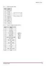
Page 21: ...V0_S 4 P_ 5V0_S 5 GND 4 2 4 SATA Power Connector Pin Header CN14 Pin Signal 1 P_ 5V0_S 2 P_ 5V0_S 3 P_ 5V0_S 4 GND 5 GND 6 GND 4 2 5 COM Pin Headers CN7 Signal Name Pin RS 232 CC Talk mode 1 DCD N A 2 DSR N A 3 RxD RS232_RX_ccTalk 4 RTS N A 5 TxD RS232_TX_ccTalk 6 CTS N A 7 DTR N A 8 RI 5V 12V 5V 12V 9 GND GND 10 NC NC ...

Page 22: ...RS 485 1 DCD Tx Tx Rx 2 DSR Tx Tx Rx 3 RxD Rx N A 4 RTS Rx N A 5 TxD N A N A 6 CTS N A N A 7 DTR N A N A 8 RI N A N A 9 GND GND GND 4 2 7 CPU Fan and System Fan Pin Signal 1 FAN_GND 2 P_ 12V_FAN 3 FAN_IN 4 FAN_OUT 4 2 8 GPU Fan Pin Signal 1 FAN_OUT 2 FAN_IN 3 P_ 12V_FAN 4 FAN_GND ...

Page 23: ...PK_RN 5 A_L_IN_R 6 GND_AUD 7 A_MIC_IN_L 8 SPK_LP 9 A_MIC_IN_R 10 SPK_LN 4 2 10 Power On Module Connector CN12 Pin Signal 1 P_ 5V0_A 2 P_ 3V3_A 3 PWR_BTN 4 LED_STANDBY 5 RST_BTN 6 POWER_ON 7 RESET_BUTTON_ALARM 8 PCH_SATS L 9 LED_TEMP_ALARM 10 GND 11 LED_FAN_ALARM 12 GND 13 P_ 12V_A 14 GND 15 BEEP_TEMP_ALARM 16 GND ...

Page 24: ...6 DCIN 7 GND 8 DCIN 4 2 13 PCB Edge Connector Pin Signal Pin Signal A1 pin 1 on bottom GND B1 pin 1 at top P_ 12V_S A2 P_ 12V_S B2 P_ 12V_S A3 P_ 12V_S B3 P_ 12V_S A4 GND B4 GND A5 JTAGE_CLK NC B5 PCH_SMB_CLK_A A6 JTAGE_DI NC B6 PCH_SMB_DAT_A A7 JTAGE_DO NC B7 GND A8 JTAGE_MS NC B8 P_ 3V3_S A9 P_ 3V3_S B9 JTAGE_RST NC A10 P_ 3V3_S B10 P_ 3V3_A A11 PCH_PLTRST L_BUF B11 X_PCIE_WAKE L A12 GND B12 NC ...

Page 25: ...26 GF_PCIEX23_RX_N B26 GND A27 GND B27 GF_PCIEX24_TX_P A28 GND B28 GF_PCIEX24_TX_N A29 GF_PCIEX24_RX_P B29 GND A30 GF_PCIEX24_RX_N B30 NC A31 GND B31 PCH_CLK_REQ7 L A32 NC B32 GND A33 NC B33 GF_PCIEX1_TX_P A34 GND B34 GF_PCIEX1_TX_N A35 GF_PCIEX1_RX_P B35 GND A36 GF_PCIEX1_RX_N B36 GND A37 GND B37 GF_PCIEX2_TX_P A38 GND B38 GF_PCIEX2_TX_N A39 GF_PCIEX2_RX_P B39 GND A40 GF_PCIEX2_RX_N B40 GND A41 G...

Page 26: ...N 5 SPI_BIOS_MISO 25 DATA 6 SPI_BIOS_MOSI 26 CLK 7 SPI_BIOS_CLK 27 OCD0A 8 3V3_LPC 28 OCD0B 9 GND 29 PWRBTN 10 BIOS_DIS0 30 SYS_RESET 11 RST 31 CB_RESET 12 CLK33_LPC 32 CB_PWROK 13 LPC_FRAME 33 SUS_S3 14 LPC_AD3 34 SUS_S4 15 LPC_AD2 35 SUS_S5 16 LPC_AD1 36 POSTWDT_DIS 17 LPC_AD0 37 SEL_BIOS 18 3 3V_SMC 38 BIOS_MODE 19 3 3V_A 39 SMC_STATUS 20 GND 40 RSVD ...

Page 27: ...GND 33 GND 8 GND 34 LVDS_A0P_1 9 GND 35 LVDS_A0N_1 10 GND 36 GND 11 N C 37 LVDS_B3P_1 12 N C 38 LVDS_B3N_1 13 LCD_SEL68_CN 39 GND 14 LVDS_I2C_CLK_CN 40 LVDS_BCKP_1 15 LVDS_I2C_DAT_CN 41 LVDS_BCKN_1 16 PNLPWR_5V_3V 42 GND 17 PNLPWR_5V_3V 43 LVDS_B2P_1 18 GND 44 LVDS_B2N_1 19 PNLPWR_5V_3V 45 GND 20 PNLPWR_5V_3V 46 LVDS_B1P_1 21 GND 47 LVDS_B1N_1 22 LVDS_A3P_1 48 GND 23 LVDS_A3N_1 49 LVDS_B0P_1 24 GN...

Page 28: ...3 4 CS01 white EVERCONN 2530 1x5P 2 5mm pitch SATA Power Connector Pin Header CN14 JVE 24W1125A 06S10 01T 0 5 CF01 beige JWT A1251H02 5P COM Pin Headers CN7 CN8 JVE 23N6850 10S10B 01G B 01 black JWT A2005H00 2Cx5P 2 0mm pitch 12V DC in Connector CN3 MOLEX 39 30 0080 natural MOLEX MOLEX 39012085 Audio Pin Header CN9 MOLEX 87832 1006 black MOLEX 511101060 2x5P 2 0mm pitch Power On Module Connector C...

Page 29: ...k CN6 ME Lock 15 16 Lock N A Undo default 4 3 5 Clear CMOS CN6 Clear CMOS 17 18 Clear CMOS N A Undo default 4 3 6 BIOS WP CN6 BIOS WP 19 20 BIOS WP N A Undo default Notes S3 and S4 not supported under operating system IAMT not supported while pairing with Q370 BIOS menu ME version information shows zero Do not install an operating system when BIOS WP is enabled Intel GbE LAN cannot update MAC addr...

Page 30: ...4 2 3 OFF JEIDA 24bpp default 4 3 9 LVDS Channel Selection SW2 LVDS Channel 1 4_ON VESA default 1 4_OFF JEIDA 2 3_ON Signal default 2 3_OFF Dual 4 3 10 HSIO Selection SW5 HSIO selection 1 8_ON CN24 lower connector support USB3 0 Default 1 8_OFF M 2 B key support USB 3 0 2 7_ON M 2 B key support SATA Default 2 7_OFF M 2 B key support PCIe BOM optional 3 6 ON M 2 B key support USB 3 0 Default 3 6 OF...

Page 31: ...I 5V 12V Selection 1 8_ON 2 7_OFF 3 6 OFF 5V 1 8_OFF 2 7_ON 3 6 OFF 12V 1 8_OFF 2 7_OFF 3 6 ON RI default 4 3 13 DIO Voltage Selection SW8 DIO Voltage Selection 1 4_ON 2 3_OFF 5V 1 4_OFF 2 3_ON 12V 1 4_OFF 2 3_OFF No power Default 4 3 14 Multi IO Voltage Selection SW9 Multi IO Voltage Selection 1 4_ON 2 3_OFF 3 3V 1 4_OFF 2 3_ON 5V 1 4_OFF 2 3_OFF No power Default ...

Page 32: ...24 Connector Pinouts This page intentionally left blank ...
Page 33: ... Driver Installation 25 5 Driver Installation Download the drivers for your system from the AMSTX CF product page at https www adlinktech com Products Industrial_Motherboards_SBCs MicroSTX_Motherboard AMSTX CF_Series ...

Page 34: ...26 Driver Installation This page intentionally left blank ...
Page 35: ...ystem Timer 04Eh 04Fh Motherboard resource 060h 062h 064h 066h 068h 06Fh 8042 equivalent keyboard 061h 063h 065h 067h NMI control and status 070h 077h Real Time Clock Controller bit 7 NMI mask 092h Reset Bit 0 Fast Gate A20 Bit 1 0A0h 0B1h 0B4h 0BDh Interrupt Controller 2 8259 equivalent 0B2h and 0B3h APM control and status port respectively 0E0h 0EFh Available 0F0h Co processor error register 2F8...

Page 36: ... Time clock N A No 9 Generic N A No 10 N A IRQ10 via SERIRQ PIRQ Note 11 N A IRQ11 via SERIRQ PIRQ Note 12 N A IRQ12 via SERIRQ PIRQ No 13 Math Processor N A No 14 Generic N A No 15 N A N A Note 6 3 2 IRQ Lines APIC Mode Table 7 IRQ Lines APIC Mode Note Table lists IRQ lines mapping when APIC mode is enabled IRQ Typical Interrupt Resource Connected to Pin Available 0 Counter 0 N A No 1 Keyboard Co...

Page 37: ...es 29 IRQ Typical Interrupt Resource Connected to Pin Available 11 N A IRQ11 via SERIRQ PIRQ No 12 N A IRQ12 via SERIRQ PIRQ No 13 Math Processor N A No 14 Generic N A No 15 N A N A No 16 511 Microsoft ACPI Compliant System N A Yes ...

Page 38: ...0 0x12 0 Internal Thermal Subsystem 0 0x14 0 Internal USB 3 1 xHCI HC 0 0x14 2 Internal Shared SRAM 0 0x15 0 Internal I 2 C Controller 0 0 0x15 1 Internal I 2 C Controller 1 0 0x16 0 Internal HECI 1 0 0x17 0 Internal SATA Controller AHCI 0 0x1C 0 Internal PCI Express Root Port 1 0 0x1D 0 Internal PCI Express Root Port 9 0 0x1D 3 Internal PCI Express Root Port 12 0 0x1E 0 Internal UART 0 0 0x1F 0 I...

Page 39: ...B 17 INTB 17 Int2 INTC 18 INTC 18 INTC 18 Int3 INTD 19 INTD 19 INTD 19 INT Line PCIe Port 1 PCIe Port 5 PCIe Port 6 PCIe Port 11 PCIe Port 17 PCIe Port 21 Int0 INTA 16 INTA 16 INTB 17 INTC 18 INTA 16 INTA 16 Int1 INTB 17 INTB 17 INTC 18 INTD 19 INTB 17 INTB 17 Int2 INTC 18 INTC 18 INTD 19 INTA 16 INTC 18 INTC 18 Int3 INTD 19 INTD 19 INTA 16 INTB 17 INTD 19 INTD 19 6 5 SMBus Slave Addresses Table 1...

Page 40: ...32 System Resources This page intentionally left blank ...
Page 41: ...the GpioLib h header file and GpioLib lib linkage library in the C project DI O functions are as follows GPIO_Init This API checks if the GPIO driver handle is valid char GPIO_Init Return value GPIO_OK on success GPIO_ERROR on failure GPI_Read This API reads the digital input DI pin status char GPI_Read UCHAR GpioNum PUCHAR data Argument GpioNum The number of a digital input pin 0 3 data The digit...

Page 42: ... register the event when there is a change in the state of a digital input pin char RegisterInterruptEvent HANDLE Event UCHAR Pin Argument Event Handle of the event waiting for interrupt notification Pin The number of an input pin Return value GPIO_OK on success GPIO_ERROR on failure ...

Page 43: ...e Yes No Yes Yes PEG Enable Disable No Yes Yes Yes Auto Enable Disable No Yes Yes Yes IGFX Disable Disable No No No Yes PEG Disable Disable No Yes No Yes Auto Disable Disable No Yes No Yes IGFX Auto Disable Yes No Yes Yes PEG Auto Disable No Yes No Yes Auto Auto Disable No Yes No Yes 8 2 MXM P3000 P5000 For four DP displays use vBIOS 86 04 70 00 3D for P3000 and vBIOS 86 04 70 00 3C for P5000 BIOS...

Page 44: ...from MXM PEG Auto Enable No Yes No Yes Auto Auto Enable No Yes No Yes IGFX Enable Disable Yes No Yes Yes PEG Enable Disable No Yes Yes Yes Auto Enable Disable No Yes Yes Yes IGFX Disable Disable No Yes No Yes PEG Disable Disable No Yes No Yes Auto Disable Disable No Yes No Yes IGFX Auto Disable Yes No Yes Yes PEG Auto Disable No Yes Yes Yes Auto Auto Disable No Yes Yes Yes ...

Page 45: ... use the BIOS setup program as the AMSTX CF Series ships with default settings that work well for most configurations Enter BIOS setup by selecting DEL when the system is powered on the POST Power On Self Test message is displayed The AMSTX CF Series controller supports one time Boot Menu allowing selection of boot device Enter the Boot Menu by selecting F7 at POST NOTES BIOS options listed are fo...

Page 46: ...e Access level CPU Configuration Graphics Configuration Power Management System Management Thermal Management Watchdog Timer Super IO Configuration Serial Console Redirection Trusted Computing S5 RTC Wake Settings NVMe Configuration Network Stack Configuration RAM Disk Configuration Network Configuration System Agent SA Configuration PCH IO Configuration Password Description Administrator Password...

Page 47: ...MRC Version Info only MRC Version GOP Version Info only GOP Version ME FW Version Info only ME FW Version 9 2 2 Main System Information Feature Options Description System Information Info only Project Name Info only Project Name 9 2 3 Main Processor Information Feature Options Description CPU Board Version Info only CPU Board Version CPU Brand String Info only CPU Brand String Stepping Info only C...

Page 48: ...ormation Runtime Statistics Feature Options Description Runtime Statistics Info only Total Runtime Info only Total Runtime Current Runtime Info only Current Runtime Power Cycles Info only Power Cycles Boot Cycles Info only Boot Cycles Boot Reason Info only Boot Reason 9 2 8 Main System Data Time Feature Options Description System Date Weekday MM DD YYYY Requires the alpha numeric entry of the day ...

Page 49: ...AMSTX CF Series BIOS Setup 41 9 2 9 Main Access level Feature Options Description Access Level Administrator User ...

Page 50: ...Processor L3 Cache size L4 Cache Info only Displays the Processor L4 eDRAM size VMX Info only VMX Supported or Not SMX TXT Info only SMX TXT Supported or Not Active Processor Cores All 1 2 3 Number of cores to enable in each processor package Intel VMX Virtualization Technology Disabled Enabled When enabled a VMM can utilize the additional hardware capabilities provided by Vanderpool Technology In...

Page 51: ...m Package C State Limit Setting Cpu Default Leaves to Factory default value Auto Initializes to deepest available Package C State Limit Tcc Activation Offset 0 63 Default 1 Offset from factory set Tcc activation temprature at which the Thermal Control Circuit must be activated Tcc will be activated at Tcc Activation Temp Tcc Activation Offset Tcc Activation Offset range is 0 to 63 9 3 2 Advanced G...

Page 52: ...TT Mode Select LVDS Backlight control function BMC Mode 0 255 Default 255 LVDS Backlight Brightness GTT Mode 0 100 Default 100 Set LVDS Backlight Brightness Percentage A change takes effect immediately 9 3 3 Advanced Power Consumption Feature Options Description Power Consumption Info only Enable ACPI Auto Configuration Disabled Enabled Enables or Disables BIOS ACPI Auto Configuration Enable Hiber...

Page 53: ...ower Consumption Power Consumption Feature Options Description Power Consumption Info only Current Input Current Info only Current Input Current Current Input Power Info only Current Input Power VIN Info only VIN VCORE Info only VCORE RTC Info only RTC 9 3 5 Advanced System Management Feature Options Description System Management Info only Version Info only SEMA Firmware Info only Version of SEMA ...

Page 54: ... Info only Power Up Watchdog Power Monitor current sense Info only Power Monitor current sense Boot Counter Info only Boot Counter 5V Input Voltage Info only 5V Input Voltage 4mR Rsense for Input Voltage Info only 4mR Rsense for Input Voltage CPU Fan Info only CPU Fan System Fan 1 Info only System Fan 1 AT ATX mode Info only AT ATX mode ACPI Thermal Trigger Info only ACPI Thermal Trigger Backlight...

Page 55: ...ptions Description BIOS Post Update Menu An update BIOS interface Choose BIOS Image An interface let user to choose BIOS image in local storage device Start Flash Start to flash BIOS 9 3 10 Advanced Thermal Management Feature Options Description Thermal Management Info only CPU Temperature Info only Current Info only Current of CPU temperature Startup Info only Startup of CPU temperature Min Info ...

Page 56: ... threshold of the Critical Trip Point Passive Cooling Trip Point Disabled 70 C 80 C 90 C 99 C This value is the temperature threshold of the Passive Cooling Trip Point 9 3 11 Advanced Thermal Management Smart Fan Feature Options Description Smart Fan Info only CPU Smart FanTemperature Source CPU Sensor CPU Smart FanTemperature Source CPU Fan Mode AUTO Smart Fan Fan Off Fan On CPU Fan Mode Trigger ...

Page 57: ...perature 0 100 Default 0 Trigger Temperature PWM Level 0 100 Default 30 PWM Level Trigger Point 2 Info only Trigger Temperature 0 100 Default 50 Trigger Temperature PWM Level 0 100 Default 45 PWM Level Trigger Point 3 Info only Trigger Temperature 0 100 Default 65 Trigger Temperature PWM Level 0 100 Default 65 PWM Level Trigger Point 4 Info only Trigger Temperature 0 100 Default 85 Trigger Tempera...

Page 58: ...d The Power Up Watchdog resets the system after a certain amount of time after power up Timeout 0 65535 Default 65535 Here you can enter the time the Power Up Watchdog should wait until it resets the system ATTENTION Pressing F12 during start up disables the Power Up Watchdog Info only RunTime Watchdog Disabled Enabled The RunTime Watchdog resets the system after a certain amount of time after pow...

Page 59: ...menu The settings specify how the host computer and the remote computer which the user is using will exchange data Both computers should have the same or compatible settings COM2 Info only Console Redirection Disabled Enabled Console Redirection enable or disable Console Redirection Settings Submenu As above 9 3 15 Advanced Console Redirection Settings COM1 2 Feature Options Description COM 1 2 Co...

Page 60: ...al can be sent to re start the flow Hardware flow control uses two wires to send start stop VT UTF8 Combo Key Support Disabled Enable Enable VT UTF8 Combination Key Support for ANSI VT100 terminals Recorder Mode Disabled Enable With this mode enabled only text will be sent This is to capture Terminal data Resolution 100x31 Disabled Enable Enables or disables extended terminal resolution Putty KeyP...

Page 61: ...sence Spec Version 1 2 1 3 Select to Tell O S to support PPI Spec Version 1 2 or 1 3 Note some HCK tests might not support 1 3 PH Randomization Disabled Enabled Enables or Disables Platform Hierarchy randomization DO NOT ENABLE THIS QUESTION IN PRODUCTION PLATFORMS THIS IS FOR DEVELOPMENT TESTING OVERRIDE ChangePlatformAuth ELINK for production platforms supporting TXT 9 3 17 Advanced S5 RTC Wake ...

Page 62: ...HTTP boot support will not be available IPSEC Certificate Disable Enable Support to Enable Disable IPSEC certificate for Ikev PXE boot wait time 0 5 Default 0 Wait time in seconds to press ESC key to abort the PXE boot Use either or numeric keys to set the value Media detect count 1 50 Default 1 Number of times the presence of media will be checked Use either or numeric keys to set the value 9 3 2...

Page 63: ...valid RAM disk size should be multiples of the RAM disk block size Create Exit Yes Create a new RAM disk with the given starting and ending address Discard Exit Yes Discard and exit 9 3 23 Advanced RAM Disk Configuration Create from file Feature Options Description Create from file Select file Create a RAM disk from a given file ...

Page 64: ...4 2 Chipset System Agent SA Configuration Memory Configuration Feature Options Description Memory Configuration Info only Memory RC Version Info only Memory RC Version Memory Frequency Info only Memory Frequency Memory Timings tCL tRCD tRP tRAS Info only Memory Timings tCL tRCD tRP tRAS DIMM 1 Info only DIMM 1 info Size Info only Size of DIMM 1 Number of Ranks Info only Number of Ranks of DIMM 1 M...

Page 65: ...ics Device 9 4 4 Chipset System Agent SA Configuration PEG Port Configuration Feature Options Description PEG Port Configuration Info only PEG Bus Dev Fun Info only PEG location and info Enable Root Port Disabled Enabled Auto Enable or Disable the Root Port Max Link Speed Auto Gen1 Gen2 Gen3 Configure PEG Bus Dev Fun Max Speed PCIe Spread Spectrum Clocking Disable Enable Allows disableing Spread S...

Page 66: ...figuration Info only PCI Express Clock Gating Disabled Enabled Enabled PCI Express Clock Gating Enable Disable for each root port Pcie Pll SSC Auto 0 0 0 1 0 2 0 3 0 4 0 5 0 6 0 7 0 8 0 9 1 0 1 1 1 2 1 3 1 4 1 5 1 6 1 7 1 8 1 9 2 0 Pcie Pll SSC percentage AUTO Keep hw default no BIOS override Range is 0 0 2 0 9 4 7 Chipset PCH IO Configuration SATA Configuration Feature Options Description SATA Co...

Page 67: ...n Selectively Enable Disable the corresponding USB port from reporting a Device Connection to the controller U3_USB1_TX_P EXTERNAL USB Disabled Enabled U3_USB2_TX_P EXTERNAL USB Disabled Enabled U3_USB3_TX_P EXTERNAL USB Disabled Enabled U3_USB4_TX_P EXTERNAL USB Disabled Enabled U3_USB5_TX_P PIN HEADER USB Disabled Enabled U3_USB6_TX_P PIN HEADER USB Disabled Enabled U2_USB1_P EXTRENAL USB Disabl...

Page 68: ...n Feature Options Description Security Configuration Info only BIOS Lock Disabled Enabled Enable Disable the PCH BIOS Lock Enable feature Required to be enabled to ensure SMM protection of flash 9 4 10 Chipset PCH IO Configuration HD Audio Configuration Feature Options Description HD Audio Configuration Info only HD Audio Disabled Enabled Control Detection of the HD Audio device ...

Page 69: ...endor Keys Info only Valid Modified Secure Boot Control Disabled Enabled Secure Boot feature is Active if Secure Boot is Enabled Platform Key PK is enrolled and the System is in User mode The mode change requires platform reset Secure Boot Mode Standard Custom Secure Boot mode options Standard or Custom In Custom mode Secure Boot Policy variables can be configured by a physically present user with...

Page 70: ...equired to launch active boot option Has no effect for BBS boot options Boot Configuration Info only Boot Option 1 Hard Disk Boot Option 2 CD DVD Boot Option 3 USB Hard Disk Boot Option 4 USB CD DVD Boot Option 5 USB Key Boot Option 6 USB Floppy Boot Option 7 USB Lan Boot Option 8 Hard Disk CD DVD USB Hard Disk USB CD DVD USB Key USB Floppy USB Lan Network Disabled Network Sets the system boot ord...

Page 71: ...tem setup without saving any changes Save Options Info only Save Changes Yes No Save Changes done so far to any of the setup options Discard Changes Yes No Discard Changes done so far to any of the setup options Restore Defaults Yes No Restore Load Default values for all the setup options Save as User Defaults Yes No Save the changes done so far as User Defaults Restore User Defaults Yes No Restor...

Page 72: ...o avoid electrical shock and or damage to equipment Keep equipment away from water or liquid sources Keep equipment away from high heat or high humidity Keep equipment properly ventilated do not block or cover ventilation openings Make sure to use recommended voltage and power source settings Always install and operate equipment near an easily accessible electrical socket outlet Secure the power c...

Page 73: ...l 1 408 360 0200 Toll Free 1 800 966 5200 USA only Fax 1 408 360 0222 Email info adlinktech com ADLINK Technology China Co Ltd Address 300 Fang Chun Rd Zhangjiang Hi Tech Park Pudong New Area Shanghai 201203 China Tel 86 21 5132 8988 Fax 86 21 5132 3588 Email market adlinktech com ADLINK Technology GmbH Address Hans Thoma Strasse 11 D 68163 Mannheim Germany Tel 49 621 43214 0 Fax 49 621 43214 30 E...

Reviews: