background image

System Description

 15

AVA-5500

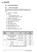
Table 2-4: AVA-5200 Power Consumption

2.6.2

System Power Features

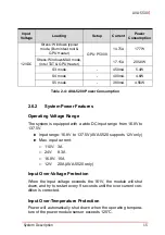
Operating Voltage Range

The system is equipped with a wide DC input range from 16.8V to
137.5V.

X

Input range: 16.8V to 137.5V (AVA-5520 supports 12V only)

X

Max. input current: 

Z

110V: 3A

Z

24V: 8.3A 

Z

16.8V: 15A

Z

12V: 20A 

(AVA-5520 

only)

Input Over-Voltage Protection

When the input voltage exceeds the 161V, the module will shut
down, and try to restart every 9 seconds until the over current con-
dition is corrected.

Input Over-Temperature Protection

Power will automatically shut down when the operating tempera-
ture of the power module sensor exceeds 125°C.

Input 

Voltage

Loading

Setup

Current

Power 

Consumption

12VDC

Stress: Windows typical 

mode, (Burnintest tool & 

GPU Heater)

GPU: P5000

14.75A

177W

Stress: Windows MAX mode, 

(Intel TAT & GPU Heater) 

17.15A

205.8W

S3 mode

-

450mA

5.4W

S4 mode

-

400mA

4.8W

S5 mode

-

380mA

4.56W

Summary of Contents for AVA-5500 Series

Page 1: ...Leading EDGE COMPUTING Manual Rev 1 1 Revision Date March 31 2020 Part No 50 1Z294 2010 AVA 5500 AI Enabled Video Analytics Platform User s Manual ...

Page 2: ...y Leading EDGE COMPUTING Revision History Revision Release Date Description of Change s 1 0 2019 09 09 Initial release 1 1 2020 03 31 SIM card slots moved to front panel add optional 4x isolated DIO add AVA 5520 content ...

Page 3: ...arising out of the use or inability to use the product or documentation even if advised of the possibility of such damages Environmental Responsibility ADLINK is committed to fulfill its social responsi bility to global environmental preservation through compliance with the European Union s Restriction of Hazardous Substances RoHS directive and Waste Electrical and Electronic Equipment WEEE direct...

Page 4: ...ve harm For more information go to www P65Warnings ca gov TrademarksProduct names mentioned herein are used for identi fication purposes only and may be trademarks and or registered trademarks of their respective companies Conventions Take note of the following conventions used throughout this manual to make sure that users perform certain tasks and instructions properly NOTE NOTE Additional infor...

Page 5: ...2 3 Block Diagram 9 2 4 Mechanical Dimensions 10 2 5 Mechanical Layout 12 2 6 Power Specifications 14 2 6 1 Power Consumption 14 2 6 2 System Power Features 15 2 7 Mini PCIe CAN Bus Module optional 16 3 Getting Started 17 3 1 Removing the Bottom Cover 17 3 2 Installing Wi Fi or Cellular Modules optional 18 3 3 Installing a M 2 2280 SATA Module optional 19 3 4 Installing micro USIM Cards optional 2...

Page 6: ...tion 44 5 3 3 System Time System Date 44 5 3 4 Board Information 45 5 4 Advanced Menu 46 5 4 1 CPU Configuration 47 5 4 2 Graphics Configuration 49 5 4 3 Power Management 49 5 4 4 System Management 50 5 4 5 Thermal Management 52 5 4 6 Watchdog Timer 52 5 4 7 CSM Configuration 53 5 4 8 Super IO Configuration 54 5 4 9 Serial Port x Configuration 54 5 4 10 Serial Console Redirection 55 5 4 11 Miscell...

Page 7: ...Table of Contents vii AVA 5500 5 5 Security Menu 61 5 5 1 Secure Boot 61 5 6 Boot Menu 62 5 7 Save Exit Menu 63 5 8 BIOS Beep Codes 63 Important Safety Instructions 65 Getting Service 67 ...

Page 8: ...viii Table of Contents Leading EDGE COMPUTING This page intentionally left blank ...

Page 9: ...gures Figure 2 1 AVA 5500 Block Diagram 9 Figure 2 2 AVA 5500 5520 Dimensions 10 Figure 2 3 AVA 5510 Dimensions 11 Figure 2 4 AVA 5500 Series Front Layout 12 Figure 2 5 AVA 5500 5200 Rear I O Layout 13 Figure 2 6 AVA 5510 Rear I O Layout 13 ...

Page 10: ...x List of Figures Leading EDGE COMPUTING This page intentionally left blank ...

Page 11: ...finition 28 Table 4 5 RJ 45 GbE Pin Definitions 29 Table 4 6 LAN LED Status Definitions 29 Table 4 7 DVI I Connector Pin Definition 30 Table 4 8 DisplayPort Pin Definition 31 Table 4 9 PS 2 Keyboard Mouse Pin Definition 31 Table 4 10 DC Power Input Pin Definition 31 Table 4 11 USB 2 0 M12 Connector Pin Definition 32 Table 4 12 CAN Bus Male DB9 Connector Pin Definition 32 Table 4 13 DIO DB9 Connect...

Page 12: ...xii List of Tables Leading EDGE COMPUTING This page intentionally left blank ...

Page 13: ...nt with its wide range DC input and isolated I O design but also provides an ideal edge solu tion for real time video graphic analysis applications that are vital to today s increasingly complex railroad operations The target applications include but are not limited to X Passenger Information Systems X Railroad Intrusion Detection X Train Station Surveillance X Onboard Video Security X Railroad Ha...

Page 14: ...B GDDR5 memory supported by AVA 5520 only X Rich I O 8x M12 GbE 4 support 7W PoE 4x RS 422 4x USB 3 0 1x DVI I 4x DisplayPort with lockable connectors Z AVA 5510 additional 2x USB 2 0 via M12 connectors X Rich Storage Options 1x M 2 SATA slot 1x CFast socket Z AVA 5500 5520 2x 2 5 SATA 6 0 Gb s drive bays Z AVA 5510 4x 2 5 SATA 6 0 Gb s drive bays X GNSS 3G 4G WLAN support via 2x Mini PCIe slots a...

Page 15: ...e X 1x Y cable for PS 2 KB MS Starter Cable Kit for AVA 5510 P N 91 95247 100E X 1x S coded M12 power supply cable X 4x PoE X coded M12 to RJ45 Ethernet cable X 4x A coded M12 to RJ 45 cable X 1x Y cable for PS 2 KB MS X 2x A coded M12 to USB 2 0 type A cable WARNING DO NOT install or apply power to equipment that is damaged or if there is missing incomplete equipment Retain the ship ping carton a...

Page 16: ...t for Europe P N 91 95247 500E X 1x Mini PCIe Cellular module SIMCOM SIM7100C PCIE GSM TD SCDMA CDMA WCDMA LTE GNSS X 2x external antennas X 2x internal RF cables S coded M12 Power Supply Cable P N 30 01324 0010 A0 Mini PCIe Cellular Module for Taiwan China SIMCOM SIM7100C PCIE GSM TD SCDMA CDMA WCDMA LTE GNSS P N 29 D0023 F000 Mini PCIe Cellular Module for Europe SIMCOM SIM7100C PCIE GSM TD SCDMA...

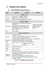
Page 17: ... I O Interfaces Ethernet 2x GbE via RJ 45 4x M12 X code 1000BASE T Ethernet ports supporting PoE Class 2 7W and 1 5kV isolation 4x M12 A coded 1000BASE T Ethernet ports 1 5kV isolation Serial Port 4x COM RS232 422 485 2kVrms isolation CAN 2x DB 9 cutouts reserved for CAN bus outputs USB 2 0 N A 2x USB 2 0 via M12 connectors N A USB 3 0 4x USB 3 0 host port Audio Mic in Line out PS 2 Keyboard Mouse...

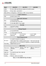
Page 18: ...x M 2 2280 SATA CFast 1x CFast socket external SATA 2x 2 5 SATA external 4x 2 5 SATA external 2x 2 5 SATA external Power Requirements DC Input 1x 4 pin S coded M12 connector 24V 36V 72V 110VDC nominal power input 16 8V to 137 5V EN50155 compliant 12V input w o wide voltage powerboard Grounding Digital chassis ground Mechanical Dimensions 360mm x 225 1mm x 88 8mm 360mm x 225 1mm x 105 4mm 360mm x 2...

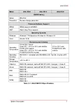
Page 19: ...to 55 C with NVIDIA P3000 GPU module Class OT3 25 C to 70 C with NVIDIA P1000 P2000 GPU module 0 C to 55 C with P3000 P5000 GPU module Operating Humidity EN 50125 1 compliant with EN 60068 2 30 Test Db 2 cycles at 55 C Storage Temperature 40 C to 85 C Vibration EN50155 standard method EN61373 2010 Category 1 Class B Shock EN50155 standard method EN61373 2010 Category 1 Class B ESD EN50153 EN50124 ...

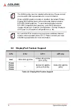
Page 20: ...tup display output to DP3 DP6 MXM graphics To send bootup display output to DP1 DP2 integrated Intel graphics go to BIOS setup and change Advanced Graphics Configuration Primary Display to IGFX see 5 4 2 Graphics Configuration on p 49 NOTE NOTE M 2 and Mini PCIe modules may require an additional thermal solution when operated above 60 C Please contact your local ADLINK representative for more info...

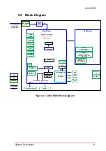
Page 21: ...CIe x2 DisplayPort from MXM x4 DVI I GbE RJ 45 x2 Ethernet M12 X code GbE x4 PoE Class 2 7Wper port 1 5kV isolation Ethernet M12 A code GbE x4 1 5kV isolation DB 9 COM x4 with 2kV isolation RS232 422 485 CAN Bus DB9 x2 PS 2 x1 USB 3 0 Type A x4 mic in line out PCIe M 2 2280 key type x1 USIM x2 MXM x1 CFast socket x1 SATA interfaces for 2 5 SSD PIS 5500 x2 PIS 5510 x4 SSD SSD SSD SSD Buttons Power ...

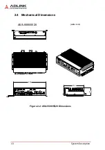
Page 22: ...10 System Description Leading EDGE COMPUTING 2 4 Mechanical Dimensions Figure 2 2 AVA 5500 5520 Dimensions AVA 5500 5520 units mm 360 6 225 1 88 8 ...

Page 23: ...System Description 11 AVA 5500 Figure 2 3 AVA 5510 Dimensions 360 225 1 105 4 6 units mm AVA 5510 ...

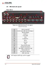
Page 24: ...code GbE B M12 X code GbE with PoE Class 2 C RS232 422 485 D USB 3 0 E RJ 45 GbE F DVI I G DisplayPort H Mic in I Line out J PS 2 K Power On Off button L System Reset button M M12 USB 2 0 AVA 5510 only N Reserved for DIO O Reserved for CAN bus P USIM card slots NOTE NOTE DP3 output is eDP only no DP support B C K L D E F G G H I M N O J P A ...

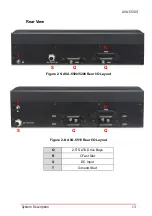
Page 25: ...System Description 13 AVA 5500 Rear View Figure 2 5 AVA 5500 5200 Rear I O Layout Figure 2 6 AVA 5510 Rear I O Layout Q 2 5 SATA Drive Bays R CFast Slot S DC Input T Ground Stud S Q Q R T S Q Q R T ...

Page 26: ...Support enabled X TurboBoost Support enabled X EIST enabled X cTDP Setting Normal X PoE full loading 4x 7W X BurnInTest Revision 8 1 1025 X TAT Revision 6 0 1011 X Windows 10 Enterprise 64 bit v1809 Table 2 3 AVA 5500 5510 Power Consumption Input Voltage Loading Setup Current Power Consumption 24VDC Stress Windows typical mode Burnintest tool GPU Heater GPU P1000 5 99A 143 9W GPU P3000 6 77A 162 6...

Page 27: ...ection When the input voltage exceeds the 161V the module will shut down and try to restart every 9 seconds until the over current con dition is corrected Input Over Temperature Protection Power will automatically shut down when the operating tempera ture of the power module sensor exceeds 125 C Input Voltage Loading Setup Current Power Consumption 12VDC Stress Windows typical mode Burnintest tool...

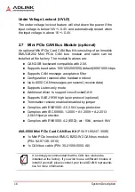
Page 28: ... after hardware reboot X Up to 6000 CAN messages per second receive data X Supports Listen only mode X Additional driver to support Linux SocketCAN X Supports SAE J1939 high layer protocol optional X Termination resistor enabled disabled by jumper X Complies with EN61000 4 5 2 5kV surge protection X Complies with IEC 60950 1 2005 A1 2009 A2 2013 2 5kV Hipot protection X Complies with EN61000 4 2 E...

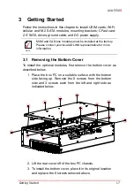
Page 29: ...he bottom cover as described below 1 Place the box PC on a suitable surface with the bottom side facing up Remove the 8 screws from the bottom side and 3 screws each from the left and right side as indicated below 2 Lift the rear cover off of the box PC chassis 3 To install the bottom cover place it in its original location and replace the 8 screws removed above NOTE NOTE MXM and CAN bus modules m...

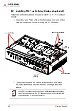
Page 30: ...o one of the slots as shown and secure it using two M2 5 screws 2 Connect the internal RF cables to the module and install the SMA connectors into the antenna openings indicated above NOTE NOTE Mini PCIe modules may require an additional thermal solution when operated above 60 C Please contact your local ADLINK representative for more information Mini PCIe modules antenna holes antenna holes Slot ...

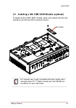
Page 31: ... install an M 2 2280 SATA module insert the module into the slot and secure it with one M2 5 screw as shown NOTE NOTE M 2 modules may require an additional thermal solution when operated above 60 C Please contact your local ADLINK rep resentative for more information M 2 module ...

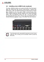
Page 32: ... the orienta tions indicated on the front panel SIM2 contacts facing down SIM1 contacts facing up with the beveled cut corner facing out wards SIM1 corresponds to Mini PCIe slot 1 CN12 and SIM2 corresponds to Mini PCIe slot 2 CN14 See 3 2 Installing Wi Fi or Cellular Modules optional on pg 18 for Mini PCIe slot locations NOTE NOTE The SIM card must be inserted with beveled cut corner facing outwar...

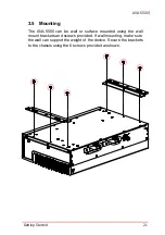
Page 33: ...g The AVA 5500 can be wall or surface mounted using the wall mount brackets and screws provided If wall mounting make sure the wall can support the weight of the device Secure the brackets to the chassis using the 6 screws provided as shown ...

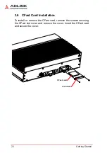
Page 34: ...Leading EDGE COMPUTING 3 6 CFast Card Installation To install or remove the CFast card remove the screws securing the CFast slot cover and remove the cover Insert the CFast card and secure the cover CFast card slot cover ...

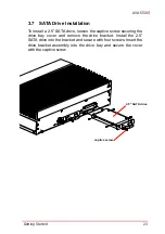
Page 35: ...ve loosen the captive screw securing the drive bay cover and remove the drive bracket Install the 2 5 SATA drive into the bracket and secure with four screws Insert the drive bracket assembly into the drive bay and secure the cover with the captive screw 2 5 SATA drive captive screw ...

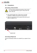
Page 36: ...and an M5 size ring terminal X Slide the ring terminal onto the ground stud and secure it with the locking M5 nut Connecting Peripherals Connect all the peripheral devices needed for your system to func tion CAUTION Connect the ground cable before making any other connec tions When disassembling the system always detach the ground cable last ground stud ...

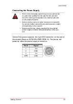
Page 37: ...ter system may only be carried out by personnel qualified for the specific task and who have the training and experience to identify risks and avoid potential hazards Z Make sure that a ground cable has been connected to the system before connecting an external power supply and switching on the system Z Make sure that the voltage supplied by the external power supply conforms with specifications o...

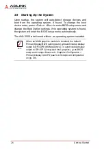
Page 38: ...erating system is found the system will enter the BIOS setup menu automatically The AVA 5500 is delivered without an operating system installed NOTE NOTE When an MXM graphics module is installed the default Primary Display BIOS setting Auto will send bootup display output to DP3 DP6 MXM graphics To send bootup display output to DP1 DP2 integrated Intel graphics go to BIOS setup and change Advanced...

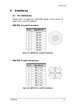
Page 39: ...nector locations GbE M12 A code Connectors Table 4 1 GbE M12 A code Pin Definition GbE M12 X code Connectors Table 4 2 GbE M12 X code Pin Definition Pin Signal Name 1 MDO0P 2 MDO0N 3 MDO1P 4 MDO1N 5 MDO3P 6 MDO3N 7 MDO2N 8 MDO2P Pin Signal Name 1 MDI_T_P0 2 MDI_T_N0 3 MDI_T_P1 4 MDI_T_N1 5 MDI_T_P3 6 MDI_T_N3 7 MDI_T_N2 8 MDI_T_P2 ...

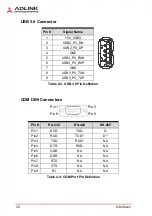
Page 40: ...ort Pin Definition Pin Signal Name 1 5V_USB3 2 USB2_P0_DN 3 USB2_P0_DP 4 GND 5 USB3_P0_RXN 6 USB3_P0_RXP 7 GND 8 USB3_P0_TXN 9 USB3_P0_TXP Pin RS 232 RS 422 RS 485 Pin1 DCD TXD D Pin2 RXD TXD D Pin3 TXD RXD NA Pin4 DTR RXD NA Pin5 GND NA NA Pin6 DSR NA NA Pin7 RTS NA NA Pin8 CTS NA NA Pin9 RI NA NA Pin 5 Pin 9 Pin 1 Pin 6 ...

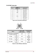
Page 41: ...0BASE T 1 TX LAN_TX0 2 TX LAN_TX0 3 RX LAN_TX1 4 LAN_TX2 5 LAN_TX2 6 RX LAN_TX1 7 LAN_TX3 8 LAN_TX3 Status Speed LED Green Amber Activity LED Yellow Network link is not established or system powered off OFF OFF 10 Mbps Link OFF ON Active Blinking 100 Mbps Link Green ON Active Blinking 1000 Mbps Link Yellow ON Active Blinking Activity Speed 8 1 ...

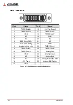
Page 42: ...t Plug Detect 2 TMDS Data2 17 TMDS Data0 3 GND 18 TMDSData0 4 NC 19 GND 5 NC 20 NC 6 DDC Clock SCL 21 NC 7 DDC Data SDA 22 GND 8 Analog vertical sync 23 TMDS Clock 9 TMDS Data1 24 TMDS Clock 10 TMDS Data1 C1 Analog Red 11 GND C2 Analog Green 12 NC C3 Analog Blue 13 NC C4 Analog Horizontal Sync 14 5 V Power C5 Analog GND Return 15 GND ...

Page 43: ...finition Pin Signal Pin Signal 1 CN_DP0_P 2 Ground 3 CN_DP0_N 4 CN_DP1_P 5 Ground 6 CN_DP1_N 7 CN_DP2_P 8 Ground 9 CN_DP2_N 10 CN_DP3_P 11 Ground 12 CN_DP3_N 13 CN_CAD L 14 CN_CEC 15 CN_AUX_P 16 Ground 17 CN_AUX_N 18 DDP_HPD 19 Ground 20 P3V3 Pin Signal Function 1 KBDATA Keyboard Data 2 MSDATA Mouse Data 3 GND Ground 4 5V Power 5 KBCLK Keyboard Clock 6 MSCLK Mouse Clock Pin Signal 1 Vin 2 GND 3 Vi...

Page 44: ...cation and pin definitions of Port 0 and Port 1 of the optional CAN Bus module are as shown below Table 4 12 CAN Bus Male DB9 Connector Pin Definition Pin Signal 1 Data 2 5V 3 NC 4 Data 5 GND Pin Port 0 Port 1 1 NC NC 2 Port 0 CAN L Port 1 CAN L 3 GND GND 4 NC NC 5 NC NC 6 NC NC 7 Port 0 CAN H Port 1 CAN H 8 NC NC 9 NC NC Port 0 Port 1 Pin 5 Pin 9 Pin 1 Pin 6 ...

Page 45: ...lated Output Channel Pin Port 0 1 1 DI0 2 DI1 3 4 DO0 5 DO1 6 DI_COM0 1 7 P_ VD0_EXT1 8 9 P 3V3_Do_GND Number of Channel 2 DI Input Voltage 0 24V dc logic H 3 3 24V logic L 0 1 5V Input Resistance 2 4kΩ 0 5W Isolated Voltage 1500VDC Number of Channel 2 DO Output Voltage 3 3VDC min 35VDC maximum Sink Current 250mA Ch Isolated Voltage 1500VDC Onboard Isolated 3 3V Output Power 200mA Port 0 Port 1 Pi...

Page 46: ... 11 REFCLK_MPCIE_N 12 UIM_CLK 13 REFCLK_MPCIE_P 14 UIM_RST 15 GND 16 UIM_VPP 17 N C 18 GND 19 N C 20 N C 21 GND 22 PLTRST_MINIPCIE L 23 MPCIE_RXN 24 P_ 3V3_MPCIE 25 MPCIE_RXP 26 GND 27 GND 28 P_ 1V5_S 29 GND 30 MPCIE_CLK 31 MPCIE_TXN 32 MPCIE_DAT 33 MPCIE_TXP 34 GND 35 GND 36 MPCIE_USB_N 37 GND 38 MPCIE_USB_P 39 P_ 3V3_MPCIE 40 GND 41 P_ 3V3_MPCIE 42 N C 43 GND 44 N C 45 N C 46 N C 47 N C 48 P_ 1V...

Page 47: ...N C 10 N C 11 GND KEY B 21 GND 20 N C 23 N C 22 N C 25 N C 24 N C 27 GND 26 N C 29 N C 28 N C 31 N C 30 N C 33 GND 32 N C 35 N C 34 N C 37 N C 36 N C 39 GND 38 NGFF_DEVSLP 41 NGFF_SATA_RXP 40 N C 43 NGFF_SATA_RXN 42 N C 45 GND 44 N C 47 NGFF_SATA_TXN 46 N C 49 NGFF_SATA_TXP 48 N C 51 GND 50 N C 53 N C 52 N C 55 N C 54 N C 57 GND 56 N C ...

Page 48: ...TING Table 4 15 M 2 Connector Pin Definition 59 N C 58 N C 61 N C 60 N C 63 N C 62 N C 65 N C 64 N C 67 N C 66 N C 69 N C 68 NGFF_SUSCLK 71 GND 70 P_ 3V3_NGFF 73 GND 72 P_ 3V3_NGFF 75 GND 74 P_ 3V3_NGFF Pin Signal Name Pin Signal Name ...

Page 49: ...imer starts the LED flashes When the timer is expired the system will auto reboot Diagnostic Green If lit continuously indicates no physical storage is connected If blinking indicates no memory is installed on either SO DIMM socket U1 White Programmable LED user defined Controlled by GPP_A21 on PCH U2 White Programmable LED user defined Controlled by GPP_A22 on PCH U3 White Programmable LED user d...

Page 50: ...wer LED lights If the system hangs depressing the button for 5 sec onds to turn off the system completely 4 4 Reset Button The reset button is a non latched The system is restarted when the button is depressed If the system hangs press the button to restart the system System status Power Button LED Idle on OS On Suspend Blinking 1Hz Hibernation Blinking 1Hz Power Off Off ...

Page 51: ...t and Power menus Setup Menu The main BIOS setup menu is the first screen that you can navi gate Each main BIOS setup menu option is described in this user s guide The Main BIOS setup menu screen has two main frames The left frame displays all the options that can be configured Grayed options cannot be configured Blue options can be The right frame displays the key legend Above the key legend is a...

Page 52: ...BIOS setup utility uses a key based navigation system called hot keys Most of the BIOS setup utility hot keys can be used at any time during the setup navigation process NOTE NOTE There is a hot key legend located in the right frame on most setup screens ...

Page 53: ...Help screen Press the F1 key to open the General Help screen F8 The F8 key on your keyboard is the previous values key It is not displayed on the key legend by default To set the previous values settings of the BIOS press the F8 key on your keyboard It is located on the upper row of a stan dard 101 keyboard The previous values settings allow the motherboard to boot up with the least amount of opti...

Page 54: ...s you have made and exit Setup Press the F10 key to save your changes The following screen will appear Press the Enter key to save the configuration and exit You can also use the Arrow key to select Cancel and then press the Enter key to abort this function and return to the previous screen ESC The Esc key allows you to discard any changes you have made and exit the Setup Press the Esc key to exit...

Page 55: ...BIOS was built MRC Version Info only w x y z Display the revision of MRC code which is implemented in BIOS VBIOS Version Info only x y zzzz VBIOS Version When video option ROM is set to Legacy Only this will display GOP Version When video option ROM is set to UEFI Only this will display ME FW Version Info only ww x yy zzzz Display the version of Intel manageability firmware which is implemented in...

Page 56: ... is booting the system CPU Frequency Info only XXXX MHz Display CPU frequency Total Memory Info only XXXX MB DDRx Display total memory size used on the motherboard and memory type Memory Frequency Info only XXXX MHz Display memory s frequency SOC SKU Info only xx Display what PCH SKU is designed on motherboard BIOS Item Options Description System Date MM DD YYYY For configuring showing system date...

Page 57: ...l time in minutes the system is running in S0 state Current Runtime Info only The returned value specifies the time in seconds the system is running in S0 state This counter is cleared when the system is removed from the external power supply Power Cycle Info only The returned value specifies the number of times the external power supply has been shut down Boot Cycles Info only The boot cycle is i...

Page 58: ...ctions Graphic Configuration Submenu For setting graphic controller parameters Power Management Submenu System Management Submenu Thermal Management Submenu Watchdog Timer Submenu CSM Configuration Submenu Super IO Configuration Submenu Serial Console Redirection Submenu Miscellaneous Submenu Network Stack Configuration Submenu Trusted Configuration Submenu Intel R Ethernet Connection 2 I219 LM 88...

Page 59: ...gy Disable Enable When enabled VMM can utilize the additional hardware capabilities provided by Vanderpool Technology C States Disable Enable Enables disables C States BIOS Item Options Description Configurable TDP Boot Mode Nominal Down Deactivate Configure TDP Mode as Nominal Down Deactivate Deactivate option will set MSR to Nominal and MMIO to Zero Configurable TDP Lock Disabled Enabled Configu...

Page 60: ... Power Limit and TDP Limit Power Limit 2 60000 Power Limit 2 in milliwatts Overclocking SKU Value must be between Max and Min Power Limits specified by PACKAGE_POWER_SKU_MSR Other SKUs This value must be between Min Power Limit and TDP Limit Power Limit 1 Time Window 0 Platform Power Limit 1 Time Window value in seconds The value may vary from 0 to 128 0 default values Indicates the time window ov...

Page 61: ...ion Enable ACPI Auto Configuration Disabled Enabled Enable disable BIOS ACPI auto configuration function Enable Hibernation Disabled Enabled Enable disable system ability to hibernate This option may be not effective with some OSes ACPI Sleep State S3 Suspend to RAM Suspend Disabled Select ACPI sleep state the system will enter when the suspend button is pressed Lock Legacy Resources Disabled Enab...

Page 62: ...o indicate that the feature is implemented on system Uptime Power Cycles Counter Info only If this item is shown it means SEMA supports Uptime Power Cycles counter System Reset Event Info only If this item is shown it means SEMA supports System Reset Event User Flash size Info only It will show 512 bytes or 1024 bytes depends on the design Watchdog Info only If this item is shown it means SEMA sup...

Page 63: ... item is shown it means SEMA supports TVIA BMC BIOS Item Options Description BMC Flags Read only Show current BMC settings BMC Select Read only Display current boot BIOS ROM chip ATX AT Mode Read only Display current power mode setting AT or ATX mode Exception Code Read only Display system exception reason BIOS Item Options Description ...

Page 64: ...emperature Current Read only Show current board temperature gotten from sensor Startup Read only Show the board temperature at system power up Min Read only Show the minimum board temperature after system boot Max Read only Show the maximum board temperature after system boot Passive Cooling Trip Point Disabled Enabled Temperature threshold of passive cooling trip point BIOS Item Options Descripti...

Page 65: ...ls what devices system can to boot Option ROM execution Info only Network Do not launch Legacy UEFI Controls the execution of UEFI and Legacy PXE OpROM Storage Do not launch UEFI Legacy Controls the execution of UEFI and Legacy Storage OpROM Video Do not launch UEFI Legacy Controls the execution of UEFI and Legacy Video OpROM Other PCI devices Do not launch UEFI Legacy For PCI devices other than N...

Page 66: ...onfiguration Submenu BIOS Item Options Description Serial Port Disabled Enabled Enable or disable serial port COMx Device Setting Info only It will show current resource assignment of serial port COMx Change Settings Auto IO 3F8 IRQ 4 IO 3F8 IRQ 3 4 5 7 9 10 11 12 IO 2F8 IRQ 3 4 5 7 9 10 11 12 IO 3E8 IRQ 3 4 5 7 9 10 11 12 IO 2E8 IRQ 3 4 5 7 9 10 11 12 Select an optimal setting for Super IO device...

Page 67: ... Redirection Settings Submenu The settings for Legacy OSes BIOS Item Options Description Terminal Type VT100 VT100 VT UTF8 ANSI Configure the type of console emulation Emulation ANSI Extended ASCII char set VT100 ASCII char set VT100 Extends VT100 to support color function keys etc VT UTF8 Uses UTF8 encoding to map Unicode chars onto 1 or more bytes Bits per second 9600 19200 38400 57600 115200 Se...

Page 68: ... both serial ports Stop bits indicate the end of a serial data packet A start bit indicates the beginning The standard setting is 1 stop bit Communication with slow devices may require more than 1 stop bit Flow Control None Hardware Software Configures flow control for console redirection Hardware flow control uses RTC CTS Software flow control uses XON XOFF VT UTF8 Combo Key Support Disabled Enab...

Page 69: ...5 Set console display resolution Redirection After POST Always Enabled BootLoader The setting specifyies if BootLoader is selected then legacy console redirection is disabled before booting to legacy OS BIOS Item Options Description PEG Port Configuration Submenu PEG Port Options SATA And RTS Configuration Submenu SATA Device Options Setting State After G3 S0 State S5 State Specify what state to g...

Page 70: ...nabled Disabled Test Mode Enable Disable Loop Back Aggressive LPM Support Enabled Disabled Enable PCH to aggressively enter link power state SATA Controller Speed Default Gen1 Gen2 Gen3 Indicates the maximum speed the SATA controller can support Serial ATA Port 0 Info only Software Preserve Info only Port X Disabled Enabled Enable Disable SATA Port Hot Plug Disabled Enabled Designates this port as...

Page 71: ...ble Enable Enable Disable DITO Configuration DITO Value Info only DM Value Info only BIOS Item Options Description Network Stack Disabled Enabled To enable or disable network stack Ipv4 PXE Support Disabled Enabled To enable or disable Ipv4 PXE boot Ipv6 PXE Support Disabled Enabled To enable or disable Ipv6 PXE boot PXE boot wait time Value Range Set wait time to press ESC key to abort the PXE bo...

Page 72: ...For configuring link speed and wake function Blink LEDs Value Range Identifies the physical network port by blinking the associated LED BIOS Item Options Description Link Speed Auto Negotiated 10 Mbps Half 10 Mbps Full 100 Mbps Half 100 Mbps Full For setting link speed of Ethernet Wake On LAN Enabled Disabled For enabling disabling wake on LAN function ...

Page 73: ...s enter without inputting password it will clear password User Password Enter to set password Configure Clear User Password When pressing enter a menu will be popped up for creating new password When password installed press enter without inputting password it will clear password Secure Boot menu Submenu BIOS Item Options Description System Mode Info only Secure Boot Info only Secure Boot Control ...

Page 74: ...ite waiting Bootup NumLock State On Off Select the keyboard NumLock state after system boot Quiet Boot Disabled Enabled Enabled will show splash screen during POST Disabled will show boot message during POST Fast Boot Disabled Enabled Enable or disabled Fast boot feature Most probes are skipped to reduce time cost during boot Boot Option 1 8 Hard Disk CD DVD USB Hard Disk USB CD DVD USB Key USB Fl...

Page 75: ...Reset Enter Discard all changed settings and let system do reset to boot system Save Changes Enter Save all changed settings Discard Changes Enter Discard changes done so far to any of the setup options Restore Default Enter Load the default made when BIOS was built Save as User Default Enter Save all changed done so far as User Defaults Restore User Default Enter Load the default that user save a...

Page 76: ...64 BIOS Setup Leading EDGE COMPUTING This page intentionally left blank ...

Page 77: ...Turn off power and unplug any power cords cables X To avoid electrical shock and or damage to equipment Z Keep equipment away from water or liquid sources Z Keep equipment away from high heat or high humidity Z Keep equipment properly ventilated do not block or cover ventilation openings Z Make sure to use recommended voltage and power source settings Z Always install and operate equipment near an...

Page 78: ...ced by authorized technicians when Z The power cord or plug is damaged Z Liquid has penetrated the equipment Z It has been exposed to high humidity moisture Z It is not functioning or does not function according to the user s manual Z It has been dropped and or damaged and or Z It has an obvious sign of breakage WARNING Risk of explosion if battery is replaced with one of an incorrect type Dispose...

Page 79: ...408 360 0200 Toll Free 1 800 966 5200 USA only Fax 1 408 360 0222 Email info adlinktech com ADLINK Technology China Co Ltd 300 Fang Chun Rd Zhangjiang Hi Tech Park Pudong New Area Shanghai 201203 China Tel 86 21 5132 8988 Fax 86 21 5132 3588 Email market adlinktech com ADLINK Technology GmbH Hans Thoma Strasse 11 D 68163 Mannheim Germany Tel 49 621 43214 0 Fax 49 621 43214 30 Email emea adlinktech...

Reviews: