background image

28

Getting Started

2. Lift and rotate the load lever to a 135° angle

3. Lift the load plate to a 100° angle using your thumb and

forefinger 

4. Use your thumb to push and remove the protective

socket cover (plastic) from the load plate 

Summary of Contents for MI-960

Page 1: ...Advance Technologies Automate the World Manual Rev 2 01 Revision Date April 14 2009 Part No 50 1X001 1010 MI 960 Mini ITX Industrial Motherboard with Intel Q965 Chipset User s Manual ...

Page 2: ...ii Revision History Revision Release Date Description of Change s 2 00 2008 11 18 Initial Release 2 01 2009 04 14 Correct graphics spec GbE pin LED def n ...

Page 3: ...en if advised of the possibility of such damages Environmental Responsibility ADLINK is committed to fulfill its social responsibility to global environmental preservation through compliance with the Euro pean Union s Restriction of Hazardous Substances RoHS direc tive and Waste Electrical and Electronic Equipment WEEE directive Environmental protection is a top priority for ADLINK We have enforce...

Page 4: ...nnectors and jumpers as well as pin assignments for configuring the MI 960 and any attached external devices Chapter 3 Getting Started Describes how to install components on the MI 960 CPU memory modules and drivers Chapter 4 BIOS Setup Presents information and illustrations to help understand and configure the system BIOS Chapter 5 POST Codes Presents POST information and detailed descriptions fo...

Page 5: ...ly NOTE NOTE Additional information aids and tips that help users perform tasks CAUTION Information to prevent minor physical injury component dam age data loss and or program corruption when trying to com plete a task WARNING Information to prevent serious physical injury component damage data loss and or program corruption when trying to complete a specific task ...

Page 6: ...vi Preface This page intentionally left blank This page intentionally left blank ...

Page 7: ... 2 Overview 2 1 3 Features 2 1 4 Specifications 3 1 5 Power Consumption 5 1 6 Block Diagram 6 1 7 Functional Description 7 1 8 Board Layout 10 1 9 Mechanical Drawings 12 2 Connectors Jumpers 15 2 1 Rear I O Connectors 15 2 2 Onboard Connectors 18 2 3 Jumpers 25 3 Getting Started 27 3 1 Installing the CPU 27 3 2 Memory Module Installation 31 3 3 Driver Installation 33 ...

Page 8: ...I PnP Settings 50 4 4 1 IRQ DMA 50 4 5 Boot Settings 51 4 5 1 Boot Settings Configuration 51 4 6 Security Setup 54 4 7 Chipset Setup 57 4 7 1 North Bridge Configuration 58 4 7 2 South Bridge Configuration 60 4 8 Exit Menu 61 5 POST Codes 63 5 1 Post Code Checkpoints 63 A Appendix Watchdog Timer 67 A 1 Sample Code 67 B Appendix System Resources 71 B 1 System Memory Map 71 B 2 Direct Memory Access C...

Page 9: ...Table of Contents ix MI 960 Important Safety Instructions 81 Getting Service 83 ...

Page 10: ...x Table of Contents This page intentionally left blank ...

Page 11: ...xi MI 960 List of Figures Figure 1 1 MI 960 Block Diagram 6 Figure 1 2 MI 960 Board Layout 10 Figure 1 3 MI 960 Rear I O Layout 11 Figure 1 4 MI 960 Board Dimensions top view 12 Figure 1 5 MI 960 Rear I O Dimensions 13 ...

Page 12: ...xii List of Figures This page intentionally left blank ...

Page 13: ... 960 Power Consumption 5 Table 5 1 POST Code Checkpoints 66 Table B 1 System Memory Map 71 Table B 2 Direct Memory Access Channels 72 Table B 3 IO Map 74 Table B 4 IRQ Lines PIC Mode 75 Table B 5 IRQ Lines APIC Mode 77 Table B 6 PCI Configuration Space Map 79 Table B 7 PCI Interrupt Routing Map 80 ...

Page 14: ...xiv List of Tables This page intentionally left blank ...
Page 15: ...0 Industrial Mini ITX Motherboard X I O shield x1 X SATA cable x2 X SATA power cable x1 X IDE cable x1 X COM cable x1 X 2 port USB cable with bracket x1 X Driver DVD X User s Manual WARNING DO NOT install or apply power to equipment that is dam aged or if there is missing incomplete equipment Retain the shipping carton and packing materials for inspection Please contact your ADLINK dealer vendor i...

Page 16: ...e diverse I O storage and audio inter faces make the MI 960 suitable for multimedia automation control transportation POS POI and medical applications requir ing a compact easy to deploy and cost effective mainboard 1 3 Features X Mini ITX form factor 170 x 170 mm X Supports the following CPUs in the LGA775 package Z Intel Core 2 Quad Duo Q6600 Q6700 Z Intel Core 2 Duo E6400 E4300 Z Intel Pentium ...

Page 17: ... 90nm 1 MB L2 3 0 GHz 800 MHz Intel Celeron Processor 440 65nm 512KB L2 2 0 GHz 800 MHz Intel Celeron D Processor 352 65nm 512KB L2 3 2 GHz 533 MHz Intel Celeron D Processor 341 90nm 512KB L2 2 93 GHz 533 MHz FSB 533 800 1066 MHz Chipset North Bridge Intel Q965 chipset South Bridge Intel ICH8 chipset Memory DDR2 533 667 800 SDRAM 4GB max 2x 240 pin DDR2 DIMM slots BIOS AMI BIOS with 16 Mb Flash RO...

Page 18: ...rts 1 D Sub VGA connector 1 serial port 2 PS2 keyboard mouse ports 3 audio jacks Expansion Slots 1 32 bit 33MHz PCI slot 1 CompactFlash socket Display VGA GMA 3000 integrated in Q965 GMCH VRAM Shared system memory up to 256 MB CRT Dsub 15 connector up to 2048x1536 75 Hz LVDS Internal 24 bit header supports dual independent display Ethernet Controller Intel 82566DM Marvell 88E8053 Ports Two RJ 45 E...

Page 19: ...480ATX 450W DOS idle Power Req 3 3V 5V 12V CPU 12V Total Current A 1 77 3 27 0 338 3 12 8 50 Watts W 5 841 16 34 4 06 37 46 63 67 Linux Idle Power Req 3 3V 5V 12V CPU 12V Total Current A 1 74 3 12 0 32 1 26 6 44 Watts W 5 75 15 58 3 89 15 14 40 35 Windows XP Idle Power Req 3 3V 5V 12V CPU 12V Total Current A 1 803 3 12 0 28 1 31 6 52 Watts W 5 95 15 62 3 42 15 72 40 71 Windows XP CPU 100 Usage Pow...

Page 20: ...ar x4 Internal x4 533 800 1066 MHz FSB DDR Channel A DDR Channel B DDRII 533 667 800 MHz PCIe x1 PCIe Controller PCIe x1 PCI Bus PCI 32 bit 33MHz bus SATA SATA ports x2 DIMM x2 Realtek ALC262 Audio Codec Audio Hardware Monitor PCI Controller Intel 82566DM RJ 45 Marvell 88E8053 RJ 45 SPI Chrontel 7308B 24 bit LVDS SATA to CF CF Socket CPU Core 2 Quad Duo Celeron LGA775 package 800 1066 MHz FSB PCIe...

Page 21: ... controller hub GMCH and the Intel ICH8 I O controller hub provides the vital interfaces for the motherboard The Intel Q965 comes with the Intel Graphics Media Accelera tor 3000 an integrated graphics engine with enhanced 3D 2D graphics rendering and video capabilities The GMCH also pro vides the interface for the processor and system memory The Intel ICH8 M Southbridge is the eighth generation of...

Page 22: ... the Intel 82566DM and Mar vell 88E8053 controllers Serial ATA Storage is efficient and secure with the Serial ATA interface Utiliz ing the Intel ICH8 the MI 960 supports up to two Serial ATA devices capable of reading writing data at up to 3 Gbps The SATA specification improves chassis airflow via thinner and more flexible cables with lower pin count Universal Serial Bus USB 2 0 The MI 960 incorp...

Page 23: ... 1 to 255 seconds or from 1 to 255 minutes The WDT generates a reset signal then a reset request after failure to strobe it within the programmed time period A register bit may be enabled to indicate if the watchdog timer caused the reset event The WDT register is cleared during the power on sequence to enable the operating system to take appropriate action when the watchdog generates a reboot ...

Page 24: ...ader FNY1 System Fan connector CN10 SATA0 connector J1 2 DIMM1 2 slot CN12 SATA1 connector J3 LVDS connector CN13 COM1 connector JP1 Case open RSVD CN14 USB6 7 pin header JP2 Clear CMOS jumper CN18 ATX power connector Slot 1 PCI slot CN19 System Panel connector CN18 CN19 CN3 J2 J1 Slot 1 CN12 CN10 FNY1 JP1 CN25 J3 JP2 CN13 CN1 FN1 CN9 CN14 CF on bottom ...

Page 25: ...Introduction 11 MI 960 Figure 1 3 MI 960 Rear I O Layout VGA COM2 MS KB CF GbE1 GbE2 USB0 USB1 USB2 USB3 Audio ...

Page 26: ...12 Introduction 1 9 Mechanical Drawings Figure 1 4 MI 960 Board Dimensions top view Dimensions in mm ...

Page 27: ...Introduction 13 MI 960 Figure 1 5 MI 960 Rear I O Dimensions Dimensions in mm ...

Page 28: ...14 Introduction This page intentionally left blank ...

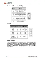
Page 29: ...I 960 Refer to Figure 1 2 MI 960 Board Layout and Figure 1 3 MI 960 Rear I O Layout for connector and jumper locations 2 1 Rear I O Connectors PS 2 Mouse Port green PS 2 Keyboard Port purple Pin Signal Function 1 MSDATA Mouse Data 2 NC not connected 3 GND Ground 4 5V Power 5 CLK Clock 6 NC not connected Pin Signal Function 1 KBDATA Keyboard Data 2 NC not connected 3 GND Ground 4 5V Power 5 CLK Clo...

Page 30: ...port connects a speaker or headphone while the pink Mic In jack connects a microphone Pin RS 232 1 DCD Data Carrier Detect 2 RXD Receive Data 3 TXD Transmit Data 4 DTR Data Terminal Ready 5 GND ground 6 DSR Data Set Ready 7 RTS Request to Send 8 CTS Clear to Send 9 RI Ring Indicator Signal Name Pin Pin Signal Name Red 1 2 Green Blue 3 4 VCC pull up GND 5 6 GND GND 7 8 GND VCC 9 10 GND VCC pull up ...

Page 31: ...d Refer to the tables below for the LAN port pin and LED definitions Refer to the table below for the LAN port LED definitions Pin Signal Name 1 Vcc 2 USB 3 USB 4 GND Pin Signal Name 1 MDI1 2 MDI1 3 MDI2 4 MDI2 5 MDI3 6 MDI3 7 MDI4 8 MDI4 LED1 LED2 Status Description Status Description Off No Link Off 10 Mb connection On Linked Green 100 Mb connection Blinking Data Activity Amber 1 Gb connection L...

Page 32: ...a 10 9 Data 4 10 Data 11 11 Data 3 12 Data 12 13 Data 2 14 Data 13 15 Data 1 16 Data 14 17 Data 0 18 Data 15 19 Ground 20 21 Request 22 Ground 23 I O Write 24 Ground 25 I O Read 26 Ground 27 I O Ready 28 Cable Select 29 DMA Ack 30 Ground 31 Interrupt Request 32 No Connect 33 Device Address 1 34 ATA 66 100 Detect 35 Device Address 0 36 Device Address 2 37 Chip Select 1 38 Chip Select 3 39 Device Ac...

Page 33: ...B0 4 USB1 5 USB0 6 USB01 7 GND 8 GND 9 Key 10 NC Pin Signal 1 GND 2 TXP 3 TXN 4 GND 5 RXN 6 RXP 7 GND Pin Signal Functions 1 DCD Data Carrier Detect 2 RXD Data Set Ready 3 TXD Receive Data 4 DTR Request to Send 5 Ground Transmit Data 6 DSR Clear to Send 7 RTS Data Terminal Ready 8 CTS Ring Indicate 9 RI Ground 10 NC No Connect 1 7 1 5 6 ...

Page 34: ...Power Connector CN18 Pin Signal Pin Signal 1 3 3V 13 3 3V 2 3 3V 14 12V 3 GND 15 GND 4 5V 16 PS ON 5 GND 17 GND 6 5V 18 GND 7 GND 19 GND 8 PWRGD 20 NC 9 5VSB 21 5V 10 12V 22 5V 11 12V 23 5V 12 24 pin detection 24 GND 1 12 13 24 ...

Page 35: ... 5V Power 5 NC 6 GND Ground Key Lock 7 KEYLOCK Keyboard lock 8 PLED Power LED signal Power LED 9 NC 10 5V Power LED pull up 11 GND Ground RESET button 12 RESETBT RESET signal 13 NC 14 GND Ground Power on button 15 POWERBT Power on signal 16 NC 17 NC 18 HDDLED Hard Disk LED signal Hard Disk LED 19 5V Hard Disk LED pull up 20 NC 1 10 20 11 ...

Page 36: ...22 Connectors Jumpers CPU Fan Connector FN1 System Fan Connector FNY1 Pin Signal 1 GND 2 Fan Power 12V 3 Fan Tachometer 4 NC Pin Signal 1 GND 2 Fan Power 12V 3 Fan Tachometer 1 3 ...

Page 37: ...t output 6 SHGND Shield GND 7 LVDS_D3P Data port output 8 SHGND Shield GND 9 SHGND Shield GND 10 LVDS_D0N Data port output 11 LVDS_CLK1P Clock port output 12 LVDS_D0P Data port output 13 LVDS_CLK1N Clock port output 14 SHGND Shield GND 15 SHGND Shield GND 16 LVDS_D1N Data port output 17 LVDS_D2P Data port output 18 LVDS_D1P Data port output 19 LVDS_D2N Data port output 20 SHGND Shield GND 1 2 20 1...

Page 38: ...F_D13 CF_D6 5 30 CF_D14 CF_D7 6 31 CF_D15 CF_CS0 7 32 CF_CS1 GND 8 33 GND GND 9 34 CF_DIOR L GND 10 35 CF_DIOW L GND 11 36 P3V3 GND 12 37 CNCF_IORDY P3V3 13 38 P3V3 GND 14 39 PCSEL GND 15 40 NC GND 16 41 CF_RESET GND 17 42 N C CF_A2 18 43 N C CF_A1 19 44 P3V3 CF_A0 20 45 N C CF_D0 21 46 N C CF_D1 22 47 CF_D8 CF_D2 23 48 CF_D9 N C 24 49 CF_D10 CD2 25 50 GND ...

Page 39: ...e and BIOS setting information CMOS is powered by the onboard button cell battery To erase the CMOS RAM data 1 Unplug the MI 960 2 Short the JP1 pin 2 3 3 Turn the power on After power on remove the jumper cap from pins 2 3 and reinstall it to pins 1 2 RTC status Connection JP2 Normal 1 2 Clear CMOS 2 3 ...

Page 40: ...26 Connectors Jumpers This page intentionally left blank ...

Page 41: ... tium Dual Core Intel Pentium 4 Intel Celeron and Intel Celeron D processors via the surface mount LGA775 socket Socket T To install the CPU 1 Press the load lever A then disengage it from the retention tab B WARNING Disconnect all power supply to the board before installing a CPU to prevent damaging the board and CPU Do not touch socket contacts Damaging the contacts voids the product warranty Fo...

Page 42: ...arted 2 Lift and rotate the load lever to a 135 angle 3 Lift the load plate to a 100 angle using your thumb and forefinger 4 Use your thumb to push and remove the protective socket cover plastic from the load plate ...

Page 43: ... on the CPU must be posi tioned on the bottom left corner of the socket 6 Carefully place the CPU on the socket in a vertical motion The socket has tabs that accommodate your fin gers during installation WARNING The CPU fits the socket in only one orientation DO NOT force it into the socket to avoid damaging it Golden triangle Notch Alignment key Socket tab ...

Page 44: ...30 Getting Started 7 Close the load plate A then fasten the load lever on the retention tab B A B ...

Page 45: ...th the same CAS latency For maximum compatibility install memory modules with the same brand model and or rating To install a memory module 1 Locate the DIMM slots on the motherboard 2 Press the socket s retaining clips outward to unlock 3 Align the memory module on the socket making sure that the notch matches the break on the socket WARNING Disconnect all power supply to the board before install...

Page 46: ...32 Getting Started 4 Insert the module firmly into the slot until the retaining clips snap back inwards and the module is securely seated ...

Page 47: ...14331 exe Follow the instructions given and reboot when instructed 4 Install the LAN1 driver Intel by running the program X Industrial Motherboard MI 960 Ethernet Intel Windows XP PRO2KXP exe Follow the instructions given and reboot if required 5 Install the LAN2 driver Marvell by running the program X Industrial Motherboard MI 960 Ethernet Marvel setup exe Follow the instructions given and reboot...

Page 48: ...34 Getting Started This page intentionally left blank ...

Page 49: ...oard 2 Press the Delete key on your keyboard when you see the following text prompt Press DEL to run Setup 3 After you press the Delete key the main BIOS setup menu displays You can access the other setup screens from the main BIOS setup menu such as Chipset and Power menus Note In most cases the Delete key is used to invoke the setup screen There are several cases that use other keys such as F1 F...

Page 50: ...e configured Grayed options cannot be configured Blue options can be The right frame displays the key legend Above the key legend is an area reserved for a text message When an option is selected in the left frame it is highlighted in white Often a text message will accompany it Navigation The BIOS setup utility uses a key based navigation system called hot keys Most of the BIOS setup utility hot ...

Page 51: ... key legend by default To set the Fail Safe settings of the BIOS press the F8 key on your keyboard It is located on the upper row of a standard 101 keyboard The Fail Safe set tings allow the motherboard to boot up with the least amount of options set This can lessen the probability of conflicting settings Hotkey Descriptions F1 The F1 key allows you to display the General Help screen Press the F1 ...

Page 52: ...us screen ESC The Esc key allows you to discard any changes you have made and exit the Setup Press the Esc key to exit the setup without saving your changes The following screen will appear Press the Enter key to discard changes and exit You can also use the Arrow key to select Cancel and then press the Enter key to abort this function and return to the pre vious screen Enter The Enter key allows ...

Page 53: ...The Main BIOS Setup screen is shown below System Time System Date Use this option to change the system time and date Highlight Sys tem Time or System Date using the Arrow keys Enter new val ues using the keyboard Press the Tab key or the Arrow keys to move between fields The date must be entered in MM DD YY format The time is entered in HH MM SS format Note The time is in 24 hour format For exampl...

Page 54: ...screen You can select any of the items in the left frame of the screen such as SuperIO Configuration to go to the sub menu for that item You can display an Advanced BIOS Setup option by highlighting it using the Arrow keys The Advanced BIOS Setup screen is shown below The sub menus are described on the following pages ...

Page 55: ...s on the right side of the screen The settings are described on the following pages An example of the IDE Configuration screen is shown below SATA Configuration This item specifies which mode the SATA channels should be initialized in The settings are Disabled Compatible and Enhanced When running in Compatible mode SATA channel can be configured as a legacy IDE channel IDE Master Slave Select one ...

Page 56: ... Serial Port1 Address Select an address and a corresponding interrupt for Serial Port1 Options 3F8 IRQ4 3E8 IRQ4 2F8 IRQ3 2E8 IRQ3 Serial Port2 Address This option specifies the base I O port address and Interrupt Request address of Serial Port2 The settings of Serial Port2 are the same as Serial Port1 However the setting used by Serial Port1 will not be available for Serial Port2 For example if S...

Page 57: ...BIOS Setup 43 MI 960 4 3 3 Hardware Health Configuration This option displays the current status of all of the monitored hard ware devices components such as voltages and temperatures ...

Page 58: ...E event will generate a sys tem wake event The options are Enabled and Disabled Resume On RTC Alarm Allows you to enable or disabled the RTC to generate a wake event When this item is set to Enabled the item RTC Alarm Date RTC Alarm Hour RTC Alarm Minute and RTC Alarm Second appear with set values Restore on AC Power Loss Determines which state the computer enters when AC power is restored after a...

Page 59: ... serial port connec tion Once both serial ports are configured to disabled you should set this value to Disabled or it may cause abnormal boot Serial Port Number Select the serial port you want to use for the remote access interface You can set the value for this option to COM1 or COM2 Note If you have changed the resource assignment of the serial ports in Advanced SuperIO Configuration you must S...

Page 60: ...t this value to turn off the redirection after POST X Boot Loader Set this value to allow the redirection to be active during POST and Boot Loader X Always Set this value to allow the redirection to be always active Terminal Type This option is used to select either VT100 VT UTF8 or ANSI terminal type The settings for this value are ANSI VT100 or VT UTF8 VT UTF8 Combo Key Support This option enabl...

Page 61: ...pport refers to USB mouse and keyboard sup port Normally if this option is not enabled any attached USB mouse or USB keyboard will not become available until a USB compatible operating system is fully booted with all USB driv ers loaded When this option is enabled any attached USB mouse or USB keyboard can control the system even when there are no USB drivers loaded on the system Set this value to...

Page 62: ...S Port 64 60 Emulation This option uses USB to receive the IO port 64 60 trap to emu late the legacy keyboard controller USB 2 0 Controller Mode The USB 2 0 Controller Mode configures the data rate of the USB port The options are FullSpeed 12 Mbps and HiSpeed 480 Mbps BIOS EHCI hand off This option provides a workaround for operating systems with out ECHI hand off support The EHCI ownership change...

Page 63: ...s they are in use on USB ports Emula tion Type can be set according to the type of attached USB mass storage device s If set to Auto USB devices less than 530MB will be emulated as Floppy and those greater than 530MB will remain as hard drive The Forced FDD option can be used to force a hard disk type drive such as a Zip drive to boot as FDD ...

Page 64: ...g and Play BIOS Setup option by highlighting it using the Arrow keys The Plug and Play BIOS Setup screen is shown below 4 4 1 IRQ DMA Set this value to allow the IRQ settings to be modified Available This setting allows the specified IRQ DMA to be used by a PCI PnP device Reserved This setting allows the specified IRQ DMA to be used by a legacy ISA device ...

Page 65: ...enu for that item You can display a Boot BIOS Setup option by highlight ing it using the Arrow keys The Boot Settings screen is shown below 4 5 1 Boot Settings Configuration Use this screen to select options for the Boot Settings Configura tion Use the up and down Arrow keys to select an item Use the and keys to change the value of the selected option The settings are described on the following pa...

Page 66: ... enabled the BIOS will display the full screen logo during the boot up sequence hiding normal POST messages When it is disabled the BIOS will display the normal POST messages instead of the full screen logo AddOn ROM Display Mode This BIOS feature controls the display of ROM messages from the BIOS of add on devices like the graphics cards or the SATA controllers during the boot sequence ...

Page 67: ...On ROM messages will only be displayed if the third party manufacturer had set the add on device to do so Bootup Num Lock This setting is to set the Num Lock status when the system is powered on Setting to On will turn on the Num Lock key when the system is powered on Setting to Off will allow users to use the arrow keys on the numeric keypad ...

Page 68: ...word every time the system boots or when Setup is exe cuted using either or either the Supervisor password or User password The Supervisor and User passwords activate two different lev els of password security If you select password support you are prompted for a one to six character password Type the password on the keyboard The password does not appear on the screen when typed Make sure you writ...

Page 69: ...word has been set Change Supervisor Password Select this option and press Enter to access the sub menu You can use the sub menu to change the supervisor password Change User Password Select this option and press Enter to access the sub menu You can use the sub menu to change the user password Clear User Password Select this option and press Enter to access the sub menu You can use the sub menu to ...

Page 70: ...User Password Select Change User Password from the Security Setup menu and press Enter Enter New Password Type the password and press Enter The screen does not dis play the characters entered Retype the password as prompted and press Enter If the password confirmation is incorrect an error message appears The password is stored in NVRAM after completes ...

Page 71: ...Setup Select the Chipset tab from the setup screen to enter the Chipset BIOS Setup screen You can select any of the items in the left frame of the screen to go to the sub menu for that item The Chipset BIOS Setup screen is shown below ...

Page 72: ...al Graphics Adapter This item is select which graphics controller to use as the pri mary boot device Options IGD Use north bridge Internal Graphics Devices IGD PCI IGD First use PCI display card if not present then use IGD PCI PEG First use PCI display card if not present then use PCIe display card PEG IGD First use PCIe display card if not present then use IGD PEG PCI First use PCIe display card ...

Page 73: ... item specifies the amount of system memory used by the Internal Graphics Device Options Enabled 8M Enabled 1M and Disabled Boot Display Device This item specifies which display port will turn on at bootup Options CRT Turn on CRT CRT LFP Turn on CRT and LFP ...

Page 74: ...o select an item Use the and keys to change the value of the selected option GbE LAN Boot Invoke the onboard LAN s PXE ROM to enable boot from LAN The options are Enabled and Disabled GbE Wake Up From S5 Set onboard LAN boot wake up from power down mode The options are Enabled and Disabled HDA Controller Set this value to Enable Disable the HDA Controller ...

Page 75: ...ng it using the Arrow keys The Exit BIOS Setup screen is shown below Save Changes and Exit When you have completed the system configuration changes select this option to leave Setup and reboot the computer so the new system configuration parameters can take effect Save Configuration Changes and Exit Now Ok Cancel appears in the window Select Ok to save changes and exit ...

Page 76: ...but may not work best for all computer applications In particular do not use the Optimal Setup options if your computer is experiencing system configuration problems Select Load Optimal Defaults from the Exit menu and press Enter Select Ok to load optimal defaults Load Failsafe Defaults Automatically sets all Setup options to a complete set of default settings when you select this option The Fails...

Page 77: ...ksum is OK Verify CMOS checksum manually by reading storage area If the CMOS checksum is bad update CMOS with power on default values and clear passwords Initialize status register A Initializes data variables that are based on CMOS setup questions Initializes both the 8259 compatible PICs in the system 05 Initializes the interrupt controlling hardware generally PIC and interrupt vector table 06 D...

Page 78: ...on of document for more information 2C Initializes different devices Detects and initializes the video adapter installed in the system that have optional ROMs 2E Initializes all the output devices 31 Allocate memory for ADM module and uncompress it Give control to ADM module for initialization Initialize language and font modules for ADM Activate ADM module 33 Initializes the silent boot module Se...

Page 79: ...needed requested Check boot password if installed 8C Late POST initialization of chipset registers 8D Build ACPI tables if ACPI is supported 8E Program the peripheral parameters Enable Disable NMI as selected 90 Initialization of system management interrupt by invoking all handlers Please note this checkpoint comes right after checkpoint 20h A1 Clean up work needed before booting to OS A2 Takes ca...

Page 80: ...r Int 19 boot Init MP tables AC End of POST initialization of chipset registers De initializes the ADM module B1 Save system context for ACPI Prepare CPU for OS boot including final MTRR values 00 Passes control to OS Loader typically INT19h Checkpoint Description ...

Page 81: ...flag IT8712_ioPort 0x4e else IT8712_ioPort 0x2e switch IT8712_ioPort case 0x2E Address port 0x2E enter keys 0x87 0x01 0x55 0x55 outportb 0x2E 0x87 outportb 0x2E 0x01 outportb 0x2E 0x55 outportb 0x2E 0x55 break case 0x4E Address port 0x4E enter keys 0x87 0x01 0x55 0xAA outportb 0x4E 0x87 outportb 0x4E 0x01 outportb 0x4E 0x55 outportb 0x4E 0xAA break default break void Exit_IT8712_Config unsigned in...

Page 82: ..._ioPort 0x07 outportb IT8712_ioPort 1 0x07 Device 7 if count_value 60 outportb IT8712_ioPort 0x72 registerValue inportb IT8712_ioPort 1 registerValue 0x7f registerValue 0x40 enable WDT output through KBRST outportb IT8712_ioPort 1 registerValue set WDT count is minute tempCount count_value 60 if count_value 60 30 tempCount if tempCount 255 tempCount 255 printf WDT timeout in d minutes n tempCount ...

Page 83: ... is Disabled n registerValue 0xbf Disable WDT output through KBRST outportb IT8712_ioPort 1 registerValue set WDT count is second outportb IT8712_ioPort 0x71 registerValue inportb IT8712_ioPort 1 registerValue 0x60 set Mouse Keyboard interrupt Enable outportb IT8712_ioPort 1 registerValue outportb IT8712_ioPort 0x73 outportb IT8712_ioPort 1 tempCount ...

Page 84: ...70 Watchdog Timer This page intentionally left blank ...

Page 85: ...ECFFFFF 1 MB APIC Configuration Space 15MB 16MB F00000 FFFFFF 1 MB ISA Hole 960 K 1024 K F0000 FFFFF 64 KB System BIOS Area 896 K 960 K E0000 EFFFF 64 KB Extended System BIOS Area 768 K 896 K C0000 DFFFF 128 KB PCI expansion ROM area C0000 C7FFF Onboard VGA BIOS CB800 CC7FFF Intel 82566DM PXE option ROM when onboard LAN boot ROM is enabled CC800 CD7FFF Marvell 88E8053 option ROM when onboard LAN b...

Page 86: ...0 1 3 is selected when using parallel port Floppy and parallel port cannot be used at the same time Channel Number Data Width System Resource 0 8 bits Parallel port 1 1 8 bits Parallel port 1 2 8 bits Diskette drive 1 3 8 bits Parallel port 1 4 Reserved cascade channel 5 16 bits Open 6 16 bits Open 7 16 bits Open ...

Page 87: ...sk 080 091 DMA page register 092 Reset Bit 0 Fast Gate A20 Bit 1 93 9F DMA page registers continued 0A0 0B1 and 0B4 0BF Interrupt controller 2 8259 equivalent 0B2 and 0B3 APM control and status port respectively 0C0 0DF DMA controller 2 8237A 5 equivalent 0E0 0EF Available 0F0 Co processor error register 0F1 N A 0F2 0F3 N A 0F4 IDE ID port 0F5 0F7 N A 0F8 IDE Index port 0F9 0FB N A 0FC IDE Data po...

Page 88: ...vailable 3F0 3F7 Primary Floppy disk controller 3F8 3FF Serial port 1 4D0 Master PIC Edge Level Trigger register 4D1 Slave PIC Edge Level Trigger register CF8 CFB PCI configuration address register 32 bit I O only CF9 Reset Control register 8 bit I O CFC CFF PCI configuration data register 400 Smbus base address for SB 480 GPIO Base Address for SB 800 PM ACPI Base Address for SB 860 Alias for ICH ...

Page 89: ...Q IRQ3 at ISA bus Note 1 4 Serial Port 1 COM1 PCI ISA IRQ4 via SERIRQ IRQ4 at ISA bus Note 1 5 Parallel Port 2 LPT2 PCI ISA IRQ5 via SERIRQ IRQ5 at ISA bus Note 1 6 Floppy Drive Controller IRQ6 via SERIRQ No 7 Parallel Port 1 LPT1 PCI ISA IRQ7 via SERIRQ IRQ7 at ISA bus Note 1 8 Real time clock N A No 9 SCI PCI IRQ9 via SERIRQ IRQ9 at ISA bus Note 1 2 10 PCI ISA IRQ10 via SERIRQ IRQ10 at ISA bus N...

Page 90: ... IRQ6 via SERIRQ No 7 Parallel Port 1 LPT1 PCI ISA IRQ7 via SERIRQ IRQ7 at ISA bus Note 1 8 Real time clock N A No 9 SCI PCI IRQ9 via SERIRQ IRQ9 at ISA bus Note 1 2 10 PCI ISA IRQ10 via SERIRQ IRQ10 at ISA bus Note 1 11 PCI ISA IRQ11 via SERIRQ IRQ11 at ISA bus Note 1 12 PS 2 Mouse PCI ISA IRQ12 via SERIRQ IRQ12 at ISA bus Note 1 13 Math Processor N A No 14 Primary IDE controller PCI ISA IRQ14 vi...

Page 91: ...up menu Note 2 BIOS does not open IRQ 9 setting for ISA bus 18 N A PCI Slot INT C UHCI Controller 2 EHCI Controller 1 SMBUS SATA controller 0 Yes 19 N A PCI Slot INT D UHCI Controller 1 SATA controller1 Yes 20 N A ICH8 internal GBE controller No 21 N A UHCI Controller 5 No 22 N A ICH8 HDA No 23 N A UHCI Controller 0 EHCI Controller 0 No IRQ Typical Intterupt Resource Connected to Pin Available ...

Page 92: ...tel ICH Express Root port 1 00h 1Ch 02h Internal Intel ICH Express Root port 2 00h 1Ch 03h Internal Intel ICH Express Root port 3 00h 1Ch 04h Internal Intel ICH Express Root port 4 00h 1Ch 05h Internal Intel ICH Express Root port 5 00h 1Dh 00h Internal Intel USB UHCI Controller 0 00h 1Dh 01h Internal Intel USB UHCI Controller 1 00h 1Dh 02h Internal Intel USB UHCI Controller 2 00h 1Dh 03h Internal ...

Page 93: ...e B 6 PCI Configuration Space Map 06h 00h 0FFh Internal PCIE Port 2 07h 00h 0FFh Internal PCIE Port 3 01h 04h 0FFh PIRQA PIRQD External PCI Slot 1 08h 00h 00h PIRQA PIRQD JMicron ATA Controller Bus Device Function Routing Description ...

Page 94: ...TA INTB INTC INTD PEG Root Port X X X X VGA X SATA Controller X X SATA Controller1 X SMBus X Thermal Controller X UHCI 0 X UHCI 1 X UHCI 2 X UHCI 3 X EHCI 0 X UHCI 4 X UHCI 5 X EHCI 0 X HDA X Intel GBE X PCIE port 0 X PCIE port 1 X PCIE port 2 X PCIE port 3 X PCI Slot1 INTA INTB INTC INTD JM363 Express IDE controller X ...

Page 95: ...urn off power and unplug any power cords cables X To avoid electrical shock and or damage to equipment Z Keep equipment away from water or liquid sources Z Keep equipment away from high heat or high humidity Z Keep equipment properly ventilated do not block or cover ventilation openings Z Make sure to use recommended voltage and power source settings Z Always install and operate equipment near an ...

Page 96: ...viced by authorized technicians when Z The power cord or plug is damaged Z Liquid has penetrated the equipment Z It has been exposed to high humidity moisture Z It is not functioning or does not function according to the user s manual Z It has been dropped and or damaged and or Z It has an obvious sign of breakage WARNING Risk of explosion if battery is replaced with one of an incorrect type Dispo...

Page 97: ...0 0222 Email info adlinktech com ADLINK Technology Beijing Address ҀᏖ ऎϞഄϰ䏃 1 োⲜ ࡼ ॺ E ᑻ 801 ᅸ 100085 Rm 801 Power Creative E No 1 B D Shang Di East Rd Beijing 100085 China Tel 86 10 5885 8666 Fax 86 10 5885 8625 Email market adlinktech com ADLINK Technology Shanghai Address Ϟ Ꮦⓩ 催 ᡔᓔথऎ䩺 䏃 333 ো 39 ᐶ 4 ሖ 200233 Tel 86 21 6495 5210 Fax 86 21 5450 0414 Email market adlinktech com ADLINK Technology S...

Page 98: ...2 Japan Tel 81 3 4455 3722 Fax 81 3 5333 6040 Email japan adlinktech com ADLINK Technology Inc Korean Liaison Office Address 昢殾柢 儛單割 嚂笊壟 60 12 壟昷捒娯 4 猻 402 笾 No 402 Dongsung B D 60 12 Nonhyeon Dong Gangnam gu Seoul 135 010 Korea Tel 82 2 2057 0565 Fax 82 2 2057 0563 Email korea adlinktech com ADLINK Technology Singapore Pte Ltd Address 84 Genting Lane 07 02A Cityneon Design Centre Singapore 349584...

Reviews: