Operation Theory
39
by 2) is used. Therefore, when the same external clock source is
applied to multiple cards, the time difference of the sampling
clocks between two cards will be half of the sampling clock period.
The A/D clock cannot synchronize the multiple cards.
5.5 A/D Data Transfer
AD Data Transfer
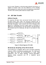
For acquiring AD data, there are several function blocks on the
PCI-9812 board. Even when the maximum sampling rate is
specified up to 20MHz, there are some limitations due to the high
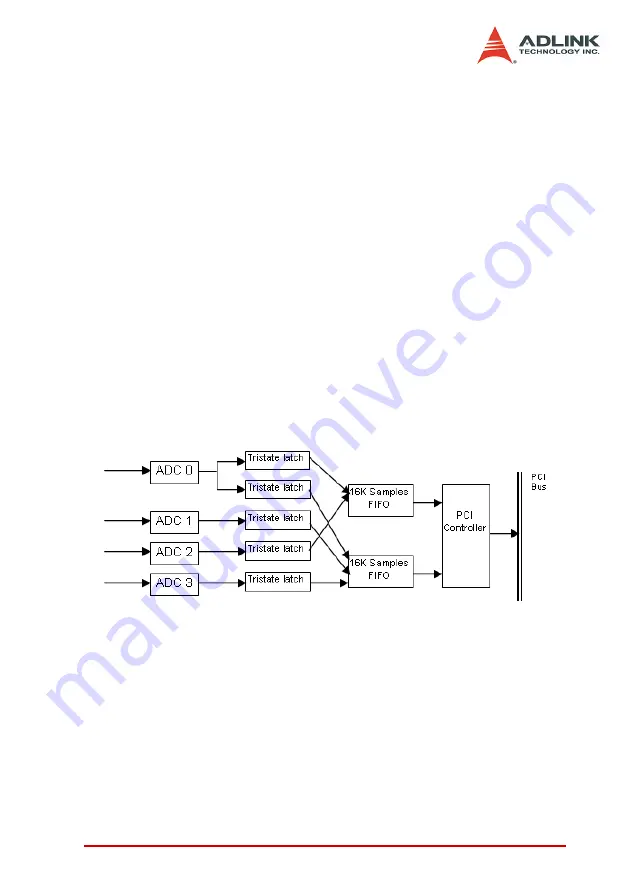
total data throughput. Users should refer to the following block
diagram to understand how the analog signal is converted to
digital form and transferred to PC host memory. The data transfer
rate limitation and the bottleneck will also be introduced in this
section.
Figure 5-5: Block Diagram of PCI-9812
Simultaneous Sampling of four AD Channels
The PCI-9812/10 is equipped with four AD converters supporting
maximum 20MHz simultaneous sampling rate. The high speed
and simple use allow the PCI-9812/9810 to serve many
applications, such as image digitizing, medical applications,
vibration testing equipment, and RF or baseband signal
digitization.
Summary of Contents for NuDAQ PCI-9810
Page 4: ......
Page 10: ...vi ...
Page 19: ...Installation 9 2 3 PCI 9812 10 s Layout Figure 2 1 PCB Layout of the PCI 9812 10 ...
Page 22: ...12 ...
Page 40: ...30 ...
Page 78: ...68 Software Utility ...


