Operation Theory
41
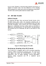
the maximum data length would be either 16K or 8K samples,
which is the maximum length from the size of onboard FIFO.
Bus-mastering Data Transfer
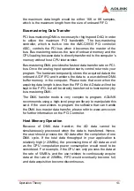
PCI bus-mastering DMA is necessary for high speed DAQ in order
to utilize the maximum PCI bandwidth. The bus-mastering
controller, which is built-in into the AMCC-5933 PCI controller
ASIC, controls the PCI bus when it becomes the master of the
bus. Bus mastering reduces the size of onboard memory and the
CPU loading because data is directly transferred to the computer’s
memory without host CPU intervention.
Bus-mastering DMA provides the fastest data transfer rate on PCI-
bus. Once the analog input operation starts, control returns to your
program. The hardware temporarily stores the acquired data in the
onboard A/D FIFO and transfers the data to a user-defined DMA
buffer memory in the computer. Please note that even when the
acquiring data length is less than the FIFO, the AD data will not be
kept in the FIFO, but will be directly transferred to host memory by
bus-mastering DMA.
The DMA transfer mode is very complex to program. ADLINK
recommends using a high-level program library to manipulate this
card. If the user wishes to program the software that can handle
the DMA bus master data transfer, please refer to www.amcc.com
for further information on the PCI Controller.
Host Memory Operation
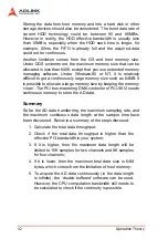
Because of DMA data transfer, the AD data cannot be
simultaneously processed when the data is transferred. Hence,
the user should process the AD data after the completion of one
DMA cycle. If the total data throughput in your application is
relatively high (>20MB/s), the processing time of AD data as well
as the CPU computation power consumption would need to be
considered. For example, if the CPU can only process the data at
the rate of 10MB/s, and the user wishes to continuously acquire
data at the rate of 20MB/s; FIFO would eventually become full,
and data acquisition become discontinuous.
Summary of Contents for NuDAQ PCI-9810
Page 4: ......
Page 10: ...vi ...
Page 19: ...Installation 9 2 3 PCI 9812 10 s Layout Figure 2 1 PCB Layout of the PCI 9812 10 ...
Page 22: ...12 ...
Page 40: ...30 ...
Page 78: ...68 Software Utility ...

