Hardware
•
15
3
Hardware Overview
This chapter describes the basic architecture of the PCI extension module and its
bus architecture.
3.1 Basic Architecture of PCI Extension Module
The PCI/PXI-8570 extension module is basically a PCI-to-PCI bridge. The
PCI-to-PCI bridge function in the PCI/PXI-8570 supports legacy address routed
traffic, which provides 100% capability with PCI drivers, application software,
BIOS, O/Ss, etc. These functions allow users to transfer their designs without
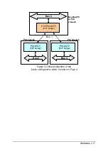
extra effort. The functional block diagram of PCI/PXI-8570 is shown in Figure 3.1.
The PCI/PXI-8570 employs a serial interconnect technology, 622Mbps low
voltage differential signaling (LVDS). Each PCI/PXI-8570 extension module has
two link ports, named as Link 0 & Link 1. Each link is divided into transmit (TX)
and receive (RX). Four TX and RX differential pairs in each link are used to
provide 2.5Gbps full duplex link bandwidth or 5Gbps of total bandwidth.
Incorporated with the high speed serial LVDS, it is easy to extend the
transmission up to 10 meters through shielded twisted pair copper cables.
Inside the PCI-to-PCI bridge, a PCI-to-StarFabric/StarFabric-to-PCI converter is
used to translate PCI transactions into StarFabric frames and StarFabric frames
into PCI transactions. The PCI interface of the PCI/PXI-8570 is capable of
64-bit/66MHz. Thus the maximum data throughput can up to 528Mbytes/s. The
PCI interface in PCI/PXI-8570 acts like the primary side of a PCI-to-PCI bridge if
PCI/PXI-8570 is plugged into the peripheral slot. The PCI interface in PXI-8570
acts like the secondary side of a PCI-to-PCI bridge if PXI-8570 is plugged into the
system slot. The secondary side PCI interface of PCI-to-PCI bridge is
responsible to the central resources and system clocks generation.


