

40
Interfaces
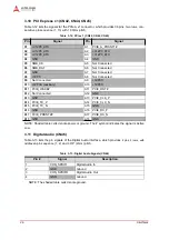
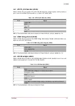
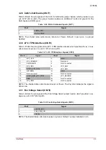
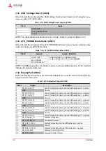
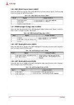
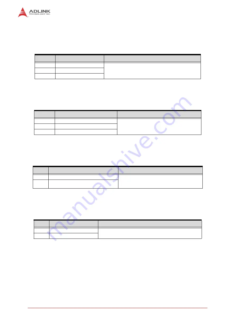
3.46 USB_VBUS Source Select (CN96)
Table 3-47 lists the pin signals of the USB_VBUS Source Select jumper header, which provides
3 pins in a single row with 2.00mm pitch.
3.47 PWM Backlight Voltage Select (CN97)
Table 3-48 lists the pin signals of the PWM Backlight Voltage Select jumper header, which pro-
vides 3 pins in a single row with 2.00mm pitch.
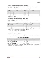
3.48 eDP1 Backlight Control (CN98)
Table 3-49 lists the pin signals of the eDP1 Backlight Control jumper header, which provides 2
pins in a single row with 2.00mm pitch.
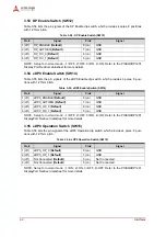
3.49 eDP1 Backlight Enable (CN99)
Table 3-50 lists the pin signals of the eDP1 Backlight Enable jumper header, which provides 2
pins in a single row with 2.00mm pitch.
Table 3-47: USB_VBUS Source Select (CN96)
Pin #
Signal
Jumper Position
1
USB_VBUS_SRC
• Jumper Installed 1-2 - USB_VBUS (
Default
)
• Jumper Installed 2-3 - USB_CC
2
USB_VBUS
3
USB_CC (Client Connect)
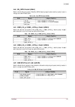
Table 3-48: PWM Backlight Voltage Select (CN97)
Pin #
Signal
Jumper Position
1
+V3P3S
• Jumper Installed 1-2 - 3.3V (
Default
)
• Jumper Installed 2-3 - 5V
2
LVDS_BKLT_CTRL_GP_PWM_OUT
3
+V5_IN
Table 3-49: eDP1 Backlight Control (CN98)
Pin #
Signal
Jumper Position
1
LVDS_BKLT_CNTRL_GP_PWM_OUT_B
• Jumper Installed - eDP1 Backlight Control
• Jumper Removed - LVDS Backlight Control
(
Default
)
2
eDP1_BKLT_CNTRL
Table 3-50: eDP1 Backlight Enable (CN99)
Pin #
Signal
Jumper Position
1
LVDS_BLEN
• Jumper Installed - eDP1 Backlight Enable
• Jumper Removed - LVDS Backlight Enable (
Default
)
2
eDP1_BKLT_EN