background image

44

Operation

the  counter  value  in  Edge  Separation  Measurement  mode  is
shown.

Figure 3-19: Mode 9-Edge Separation Measurement

Mode 10: PWM Output

The USB-1900 Series timer/counter can also simulate a PWM
(Pulse Width Modulation) output. By setting a varying amount
of  Pulse_initial_cnt  and  Pulse_length_cnt,  varying  pulse  fre-
quencies (Fpwm) and duty cycles (Dutypwm) can be obtained.
PWM output is shown.

Figure 3-20: Mode 10-PWM Output

Calculation of the PWM frequency and duty cycle is as follows.

1 3

1 3

1 2

1 1

9

8

7

6

S o f t w a r e  s t a r t

5

4

3

2

1

1

1

1

1

1

G a t e

C L K

A U X

C o u n t  v a l u e

1 0

T I M E B A S E

P W M O U T

P u l s e _ I n i t i a l _ c n t

= 0 x 7

P u l s e _ I e n g t h _ c n t = 0 x B

cnt

length

Pulse

cnt

initial

Pulse

cnt

length

Pulse

Duty

cnt

length

Pulse

cnt

initial

Pulse

F

F

PWM

Tim ebase

PWM

_

_

_

_

_

_

_

_

_

_

+

=

+

=

Summary of Contents for USB-2401

Page 1: ...Advance Technologies Automate the World Manual Rev 2 00 Revision Date Apr 27 2012 Part No 50 1Z101 1000 USB 2401 24 bit 2kS s USB 2 0 Based Universal Input DAQ Module User s Manual...

Page 2: ...ii Revision History Revision Release Date Description of Change s 2 00 Apr 27 2012 Initial release...

Page 3: ...en if advised of the possibility of such damages Environmental Responsibility ADLINK is committed to fulfill its social responsibility to global environmental preservation through compliance with the...

Page 4: ...OTE NOTE Additional information aids and tips that help users perform tasks CAUTION Information to prevent minor physical injury component dam age data loss and or program corruption when trying to co...

Page 5: ...ns 2 1 4 2 General Analog Input 2 1 4 3 Analog Input Electrical 4 1 4 4 Digital Input Output 7 1 5 Software Support 8 1 6 Driver Support for Windows 8 1 7 Utilities for Windows 10 1 8 Overview and Dim...

Page 6: ...e and Half Bridge Input Mode 30 3 3 4 Thermocouple Input Mode 31 3 3 5 RTD Input Mode 32 3 3 6 Wire Resistance Mode 34 3 4 AI Data Format 35 3 5 ADC Sampling Rate 36 3 5 1 Software Polling Data Transf...

Page 7: ...ount Apparatus 25 Figure 3 1 USB 2401 Functional Block Diagram 27 Figure 3 2 Ground Referenced Source and Differential Input 28 Figure 3 3 Floating Source and Differential Input 29 Figure 3 4 Current...

Page 8: ...viii List of Figures This page intentionally left blank...

Page 9: ...Table 1 2 USB 2401 Pin Assignment 18 Table 1 3 I O Signal Description 19 Table 3 1 Analog Input Range and Output Digital Code 35 Table 3 2 Analog Input Range and Output Digital Code cont d 36 Table 3...

Page 10: ...x List of Tables This page intentionally left blank...

Page 11: ...wall mounting The USB 2401 is suitable for basic measurement applications requiring high resolution and accuracy laboratory research and material testing environments and industrial temperature mea su...

Page 12: ...49 X 1 61 in I O Connector Two 20 pin removable screw down terminals Power requirement USB power 5 V 400 mA Operating environment Ambient temperature 0 to 55qC Relative humidity 10 to 90 non condensi...

Page 13: ...5mA for Resistance mode Cold junction compensation CJC accuracy 0 5 C after 15 minute warmup Operational common mode voltage range Voltage input mode Vcm Vpp 2 input range 25V 12 5V 2 5V 0 3125V Curre...

Page 14: ...idge 28 00370355 30 90013157 Half bridge 33 48025514 1 750342188 Thermocouple 62 9978196 0 164409864 2 wire RTD 2 842575758 0 522492944 3 wire RTD 2 879839489 0 258840329 4 wire RTD 2 902723485 0 0186...

Page 15: ...Voltage 25V 1 620950284 0 105635778 Voltage 12 5V 1 584251894 0 11027477 Voltage 2 5V 1 701225379 0 067356314 Voltage 312 5mV 20 52684091 0 113061874 Current 20mA 3 771356399 0 338399386 Full bridge 3...

Page 16: ...41 628525 67 98029188 Thermocouple 28 24161013 41 73502813 51 59679 76 21635225 2 wire RTD 8 00126525 11 64115513 16 869046 33 30653975 3 wire RTD 8 407154625 12 01619113 16 528028 33 69525963 4 wire...

Page 17: ...TL single end supports 3 3V and 5 V DI but 3 3V DO Input voltage Logic low VIL 0 8 V max IIL 0 2 mA max Logic high VIH 2 0 V min IIH 0 2 mA max Output voltage Logic low VOL 0 5 V max IOL 10 mA max Log...

Page 18: ...t kernel drivers for customized DAQ application development USB DASK enables you to perform detailed operations and achieve superior perfor mance and reliability from your data acquisition system DASK...

Page 19: ...Introduction 9 USB 2401 Please note that only DAQPilot versions 2 3 0 712 and later can support the USB 2401...

Page 20: ...to providing data collection and monitoring functions U Test also supports basic FFT analysis and provides direct control of analog output and digital I O with a user friendly interface Figure 1 1 U...

Page 21: ...Introduction 11 USB 2401 1 8 Overview and Dimensions 1 8 1 Module Figure 1 2 USB 2401 Module Rear View NOTE NOTE All dimensions shown are in millimeters mm 41 3 114...

Page 22: ...12 Introduction Figure 1 3 USB 2401 Module Side View...

Page 23: ...Introduction 13 USB 2401 Figure 1 4 USB 2401 Module Front View 41 3 114...

Page 24: ...dule in the stand slide the module body into the stand until a click is heard To remove the module from the stand twist the bottom of the stand in a back and forth motion and separate from the module...

Page 25: ...Introduction 15 USB 2401 Figure 1 7 Module In Stand Front View...

Page 26: ...16 Introduction Figure 1 8 Module Stand Top View 20 4 20 4 B 26...

Page 27: ...Introduction 17 USB 2401 Figure 1 9 Module Stand Side Cutaway View Figure 1 10 Module Stand Front View 5 89 1 5 6 3 4 100...

Page 28: ...iption as follows Table 1 2 USB 2401 Pin Assignment Pin Function Pin Function 20 GPO0 40 GPO1 19 GPI1 39 GPI3 18 GPI0 38 GPI2 17 NC 37 DGND 16 GND1 36 GND3 15 SC1 35 SC3 14 SC1 34 SC3 13 EXC1 33 EXC3...

Page 29: ...nnected on board AI 0 4 GND I Differential analog Input channels 0 3 CI 0 4 GND I Current input channel 0 3 EXC 0 3 GND O Excitation output for channel 0 3 can be configured to voltage output 2 5V or...

Page 30: ...20 Introduction This page intentionally left blank...

Page 31: ...nd 6 sec onds to load the firmware When loading is complete the LED indicator on the rear of the USB DAQ module changes from amber to green and the New Hardware message closes 4 The USB 2401 module ca...

Page 32: ...2 2 Device ID A rotary control on the rear of the module as shown controls device ID setting and can be set from 1 to 8 The device ID allows dedicated control of the USB 2401 module irrespective of th...

Page 33: ...programmable including sampling update rate input output channel input range and others Please see the UD DASK Function Reference manual for details 2 4 Device Mounting 2 4 1 Rail Mounting The multi...

Page 34: ...24 Getting Started Figure 2 4 Module Pre Rail Mounting Figure 2 5 Module Rail Mounted...

Page 35: ...ounting The multi function stand can be fixed to a wall using four flush head screws as shown The four screw holes should be approximately 3 4 mm in diameter Figure 2 6 Wall Mount Holes Figure 2 7 Mod...

Page 36: ...26 Getting Started This page intentionally left blank...
Page 37: ...Functional Block Diagram 3 2 Signal Sources 3 2 1 Floating Signal Source Not connected in any way to the existing ground system Devices with isolated output are floating signal sources such as optical...

Page 38: ...s follow 3 3 1 Voltage Input Mode The properties of the signal to be measured must be considered The differential input mode provides two inputs that respond to signal voltage difference between them...

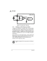
Page 39: ...3 3 Floating Source and Differential Input 3 3 2 Current Input Mode Current signal source can be floating or grounded reference converted to voltage through a precision 249 5 resistor Cross voltage on...

Page 40: ...nd half bridge modes For half bridge transducer USB 2401 has built in precision 20k resistors to compensate the circuit as a full bridge transducer measurement Also provided is a moving average functi...

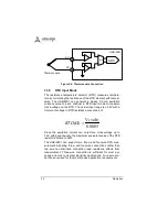
Page 41: ...of the pair of conductors The USB 2401 uses 78 125mV input range to acquire the thermocouple signal and provides a precision built in digital temperature sensor for cold junction com pensation CJC CJC...

Page 42: ...sistance conversion of Since the excitation current can only drive cross voltage up to 1 5V with good linearity the maximum equivalent value of the RTD resistor is limited to 3k The USB 2401 can suppo...

Page 43: ...Operation 33 USB 2401 Figure 3 7 4 Wire RTD Connection Figure 3 8 3 Wire RTD Connection MUX 0 5mA RTD EXC SC SC GND MUX 0 5mA RTD SC SC GND EXC...

Page 44: ...be measured and use a 2 5V input range to acquire cross voltage on the resistor The formula of voltage to resistance conversion is Since the excitation current can only drive the cross voltage up to 1...

Page 45: ...ut Digital Code Description Bipolar Analog Input Range Digital Code Full scale range 25 V 12 5 V 2 5 V 0 3125V N A Least significant bit 2 98uV 1 49uV 0 298uV 0 037uV N A FSR 1LSB 24 999997 V 12 49999...

Page 46: ...nd is suitable for retrieving the latest data without FIFO buffering latency The USB 2401 con tinuously updates the latest acquired data onto a data port for spe cific channels Data not retrieved in t...

Page 47: ...128 in continuous acquisition mode Please refer to UD DASK function reference for details of corresponding software API instruction 3 6 Programmable Function I O The USB 2401 supports powerful program...

Page 48: ...put GPTC_CLK gate input GPTC_GATE and up down control input GPTC_UD The GPTC_CLK input provides a clock source input to the timer coun ter Active edges on the GPTC_CLK input increment or decrement the...

Page 49: ...n Current count value can be read back by software any time with no influence on calcula tion GPTC_GATE enables disables calculation When GPTC_GATE is inactive the counter halts the current count valu...

Page 50: ...tware application After software start the counter calculates the number of active edges on GPTC_CLK when GPTC_GATE is in its active state After the completion of the pulse width interval on GPTC_GATE...

Page 51: ...gle pulse with a pulse delay of two and a pulse width of four is shown Figure 3 14 Mode 4 Single Gated Pulse Mode 5 Single Triggered Pulse This mode generates a single pulse with programmable delay an...

Page 52: ...h of four is shown Figure 3 16 Mode 6 Re Triggered Single Pulse Mode 7 Single Triggered Continuous Pulse Generation This mode is similar to Mode 5 except that the counter gener ates continuous periodi...

Page 53: ...Mode 9 Edge Separation Measurement Measures the time differentiation between two different pulse signals The first pulse signal is connected to GPTC_GATE and the second signal is connected to GPTC_AU...

Page 54: ...uencies Fpwm and duty cycles Dutypwm can be obtained PWM output is shown Figure 3 20 Mode 10 PWM Output Calculation of the PWM frequency and duty cycle is as follows 1 3 1 3 1 2 1 1 9 8 7 6 S o f t w...

Page 55: ...f the TrimDACs firmware are written to the onboard EEPROM TrimDACs firmware is the algorithm in the FPGA Loading calibration constants entails loading the values of TrimDACs firmware stored in the onb...

Page 56: ...46 Calibration This page intentionally left blank...

Page 57: ...urn off power and unplug any power cords cables X To avoid electrical shock and or damage to equipment Z Keep equipment away from water or liquid sources Z Keep equipment away from high heat or high h...

Page 58: ...iced by authorized technicians when Z The power cord or plug is damaged Z Liquid has penetrated the equipment Z It has been exposed to high humidity moisture Z It is not functioning or does not functi...

Page 59: ...il info adlinktech com ADLINK Technology China Co Ltd Address 300 201203 300 Fang Chun Rd Zhangjiang Hi Tech Park Pudong New Area Shanghai 201203 China Tel 86 21 5132 8988 Fax 86 21 5132 3588 Email ma...

Page 60: ...o Dong Seocho Gu Seoul 137 070 Korea Tel 82 2 2057 0565 Fax 82 2 2057 0563 Email korea adlinktech com ADLINK Technology Singapore Pte Ltd Address 84 Genting Lane 07 02A Cityneon Design Centre Singapor...

Reviews: