PCIE-1840 User Manual
24
A.5
Dynamic Characteristics
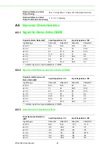
A.5.1
Signal
‐
to
‐
Noise
Ratio
(SNR)
A.5.2
Signal
‐
to
‐
Interference
and
Noise
Ratio
(SINAD)
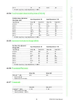
A.5.3
Total
Harmonic
Distortion
(THD)
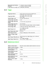
External Reference Clock
Output Swing
Min. 1.0 Vpp; Max. 1.9 Vpp, 100 Ohm load line-to-line
External Reference Clock
Output common mode voltage
1.8 ~ 2.1 V, typically
Signal-to-Noise Ratio (dB)
*
Input Impedance: 50
Input Impedance: 1M
Input Range
Filter ON
Filter OFF
Filter ON
Filter OFF
±10.0 V
N/A
N/A
72.5
65
±5.0 V
71
64
70
63.5
±2.0 V
67
61.5
65
61.5
±1.0 V
71.5
64.5
71
64
±0.5 V
70
63.5
69.5
63
±0.2 V
66
61
64
60.5
±0.1 V
61
58.5
58.5
57
* 100 kHz input tone, input amplitude is -1 dBFS.
Signal-to-Interference and
Noise Ratio (dB)
*
Input Impedance: 50
Input Impedance: 1M
Input Range
Filter ON
Filter OFF
Filter ON
Filter OFF
±10.0 V
N/A
N/A
69
64
±5.0 V
71
64
68.5
63.5
±2.0 V
67
61.5
65
61.5
±1.0 V
71.5
64
71
64
±0.5 V
69.5
63.5
69
63
±0.2 V
65.5
61
64
60
±0.1 V
61
58.5
58.5
57
* 100 kHz input tone, input amplitude is -1 dBFS.
Total Harmonic Distortion
(dB)*
Input Impedance: 50
Input Impedance: 1M
Input Range
Filter ON
Filter OFF
Filter ON
Filter OFF
±10.0 V
N/A
N/A
-71.5
-71.5
±5.0 V
-85
-83.5
-74
-75
±2.0 V
-84
-82.5
-80
-83
±1.0 V
-83
-82
-84
-82.5
±0.5 V
-83
-82.5
-85
-84
±0.2 V
-83
-83.5
-83
-83
Summary of Contents for PCIE-1840
Page 1: ...User Manual PCIE 1840 4 ch 16Bit 125 MS s High Speed Data Acquisition PCI Express Card ...
Page 4: ...PCIE 1840 User Manual iv ...
Page 12: ...PCIE 1840 User Manual 6 ...
Page 13: ...Chapter 2 2 Installation ...
Page 18: ...PCIE 1840 User Manual 12 ...
Page 26: ...PCIE 1840 User Manual 20 ...
Page 27: ...Appendix A A Specifications ...
Page 35: ...Appendix B B Block Diagram ...


