PCM-9362 User Manual
56
–
Click the READ GPIO DATA button and the status of the GPIO pin will be dis-
played in (R/W) Result field.
Test Read Multiple Input Pin
–
Click the radio button- Multiple-Pins.
–
Key in the pin number from ‘0x01’ to ‘0x0F’ to read the value of the input pin.
The pin numbers are ordered bitwise, i.e. bit 0 stands for GPIO 0, bit 1 stands
for GPIO 1, etc. For example, if you want to read pin 0, 1, and 3, the pin num-
bers should be ‘0x0B’.
–
Click READ GPIO DATA button and the statuses of the GPIO pins will be dis-
played in (R/W) Result field.
Test Write Single Output Pin
–
Click the radio button- Single-Pin.
–
Key in the pin numbers you want to write. Pin numbers start from '0'.
–
Key in the value either '0' or '1' in (R/W) Result field to write the output pin you
chose above step.
–
Click the WRITE GPIO DATA button to write the GPIO output pin.
Test Write Multiple Output Pins
–
Click the radio button- Multiple-Pins.
–
Key in the pin number from ‘0x01’ to ‘0x0F’ to choose the multiple pin num-
bers to write the value of the output pin. The pin numbers are ordered bit-
wise, i.e. bit 0 stands for GPIO 0, bit 1 stands for GPIO 1, etc. For example, if
you want to write pin 0, 1, and 3, the pin numbers should be ‘0x0B’.
–
Key in the value in (R/W) Result field from ‘0x01’ to ‘0x0F’ to write the value
of the output pin. The pin numbers are ordered bitwise, i.e. bit 0 stands for
GPIO 0, bit 1 stands for GPIO 1, etc. For example, if you want to set pin 0
and 1 high, 3 to low, the pin number should be ‘0x0B/, and then you should
key in the value ‘0x0A’ to write.
–
Click the WRITE GPIO DATA button to write the GPIO output pins.
I
2
C
When the application is executed, you can read or write a byte of data through I2C
devices. All data must be read or written in hexadecimal system.
Read a byte
–
Key in the slave device address in Slave address field.
–
Key in the register offset in Register Offset field.
–
Click the READ A BYTE button and then a byte of data from the device will
be shown on the Result field.
Summary of Contents for PCM-9362 Series
Page 8: ...PCM 9362 User Manual viii...
Page 14: ...PCM 9362 User Manual 6...
Page 24: ...PCM 9362 User Manual 16 2 3 2 Board Dimension Figure 2 3 Board Dimension layout Component side...
Page 26: ...PCM 9362 User Manual 18...
Page 27: ...Chapter 3 3 BIOS settings...
Page 35: ...27 PCM 9362 User Manual Chapter 3 BIOS settings 3 3 5 ACPI Settings Figure 3 8 ACPI Settings...
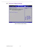
Page 50: ...PCM 9362 User Manual 42 3 7 Advanced Chipset Settings Figure 3 23 Advanced Chipset Settings...
Page 56: ...PCM 9362 User Manual 48...
Page 57: ...Chapter 4 4 S W Introduction Installation...
Page 69: ...Appendix A A PIN Assignments...
Page 99: ...91 PCM 9362 User Manual Appendix A PIN Assignments...

