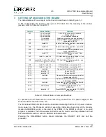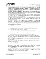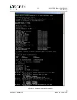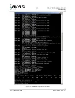
19
GR-UT699 Development Board
User Manual
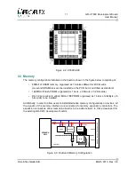
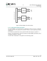
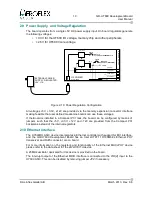
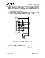
2.9 Power Supply and Voltage Regulation
The board operates from a 5V DC power supply input. On board regulators generate
the following voltages:
•
+3.3V for the UT699 I/O voltage, memory chip and other peripherals
•
+2.5V for UT699 Vcore voltage
All vo5V, +3.3V, ±12V are provided via the memory expansion connector interface
making feasible that user defined mezzanine boards can use these voltages.
If the Board is installed in a Compact PCI rack, the board can be configured by means of
jumpers such that the +5V, +3.3V, +12V and -12V are provided from the Compact PCI
backplane instead of the internal regulators.
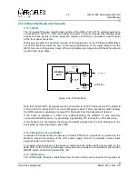
2.10 Ethernet Interface
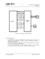
The
UT699RH
ASIC device incorporates a Ethernet controller with support for MII interface,
and the
GR-UT699
Development Board has an Intel LXT971 10/100Mbit/s Ethernet PHY
transceiver and RJ45 connector are on board.
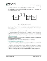
For more information on the registers and functionality of the Ethernet MAC+PHY device
please refer to the data sheet for the
WJLXT971A
device.
A 25MHz oscillator dedicated for this device is provided on the board.
The interrupt output of the Ethernet MDIO interface is connected to the
PIO[4]
input to the
UT699
ASIC. This can be disabled by removing jumper
JP2
if necessary.
© Aeroflex Gaisler AB
March 2013, Rev. 0.6
Figure 2-10: Power Regulation Configuration
REGULATOR
+3.3V
Vcore
(+2.5V for UT699RH core)
EXTERNAL POWER
SUPPLY, REGULATED
+5V, >1A
J13 POWER
2.1mm JACK
C
P
C
I
C
O
N
N
E
C
T
O
R
+5V PCI
REGULATOR
+3.3V PCI
1
1
2
3
2
3
JP12
JP13
+VIO PCI
n.c.
±12V PCI
MEZZ. CONN.
+3V3asic
(+3.3V for UT699RH)
JP14
JP15

