21
GR-UT699 Development Board
User Manual
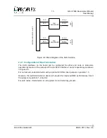
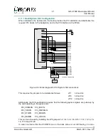
2.11.1 Host/System Slot Configuration
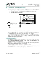
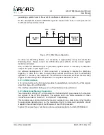
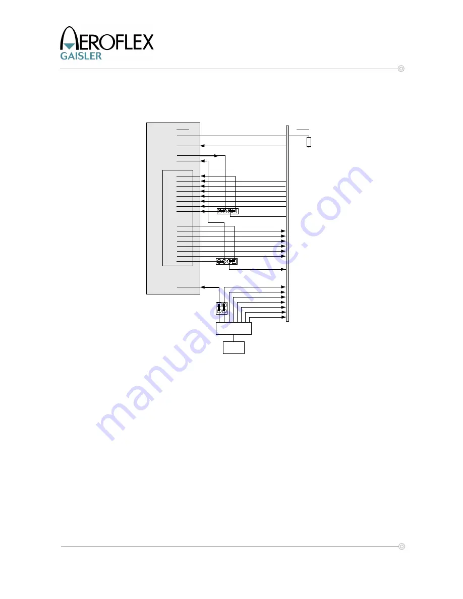
When installed in the System slot, the board provides the PCI arbitration and distributes the
required PCI clocks to the backplane, and to the PCI interface in the FPGA.
Figure 2-12: Block diagram for PCI System Slot connections
This requires the jumpers to be installed as follows:
JP7
1-2 and 3-4
JP9
1-2 and 3-4
JP10
1-2 and 3-4
Additionally, the PCI specification requires that the following system signals are pulled-up by
the card operating in the system slot:
PCI_FRAMEN
PCI_IRDYN
PCI_TRDYN
PCI_DEVSELN
PCI_STOPN
PCI_PERRN
PCI_SERRN
PCI_LOCKN
This can be achieved by installing the JP8 jumpers 1-2, 3-4, 5-6, 7-8, 9-10, 11-12, 13-14, 15-
16, 17-18 and 19-20.
In order to ensure that the PCIRSTN pin on the back plane is not left floating, it is also
© Aeroflex Gaisler AB
March 2013, Rev. 0.6
ASIC
BUFFER
XTAL
33MHz
JP7
PCICLK1
PCICLK2
PCICLK
PCICLKIN
GNT3
GNT0
GNT2
GNT1
REQ
IDSEL
GNTN
IDSEL
GNT1N
REQ4
REQ3
REQ1
REQ5N
REQ2N
REQ3N
GNT
A
R
B
IT
E
R
CPCI EDGE CONNECTOR
JP9
HOST
PCICLK4
PCICLK5
PCICLK3
PCICLK6
GND
GNT7
GNT6
GNT5
JP10
GNT4
GNT2N
GNT3N
GNT4N
GNT5N
GNT6N
REQ2
REQ1N
REQ0
REQ4N
REQ7
REQ6
REQ5
REQN
REQ6N
3
4
1
2
1
4 3 2
1
4 3 2
SYSEN


