background image


9


/W controls read and write operation. During a read cycle, /G must be asserted to enable the outputs. 
 

Table 6. Write Enable LEON-3FT J7 to J9 connector 

LEON-3FT connector 

(J9) 

UT8MR8M8 Device 

(J7) 

Pin 

Signal Pin 

Signal 

46 

WEB 

42 

/W 


5.6


Output Enable (/G) 


/W controls read and write operation. During a read cycle, /G must be asserted to enable the outputs. 
 

Table 7. Output Enable LEON-3FT J7 to J9 connector 

LEON-3FT connector 

(J9) 

UT8MR8M8 Device 

(J7) 

Pin 

Signal Pin 

Signal 

47 

OEB 

53 

/G 


5.7


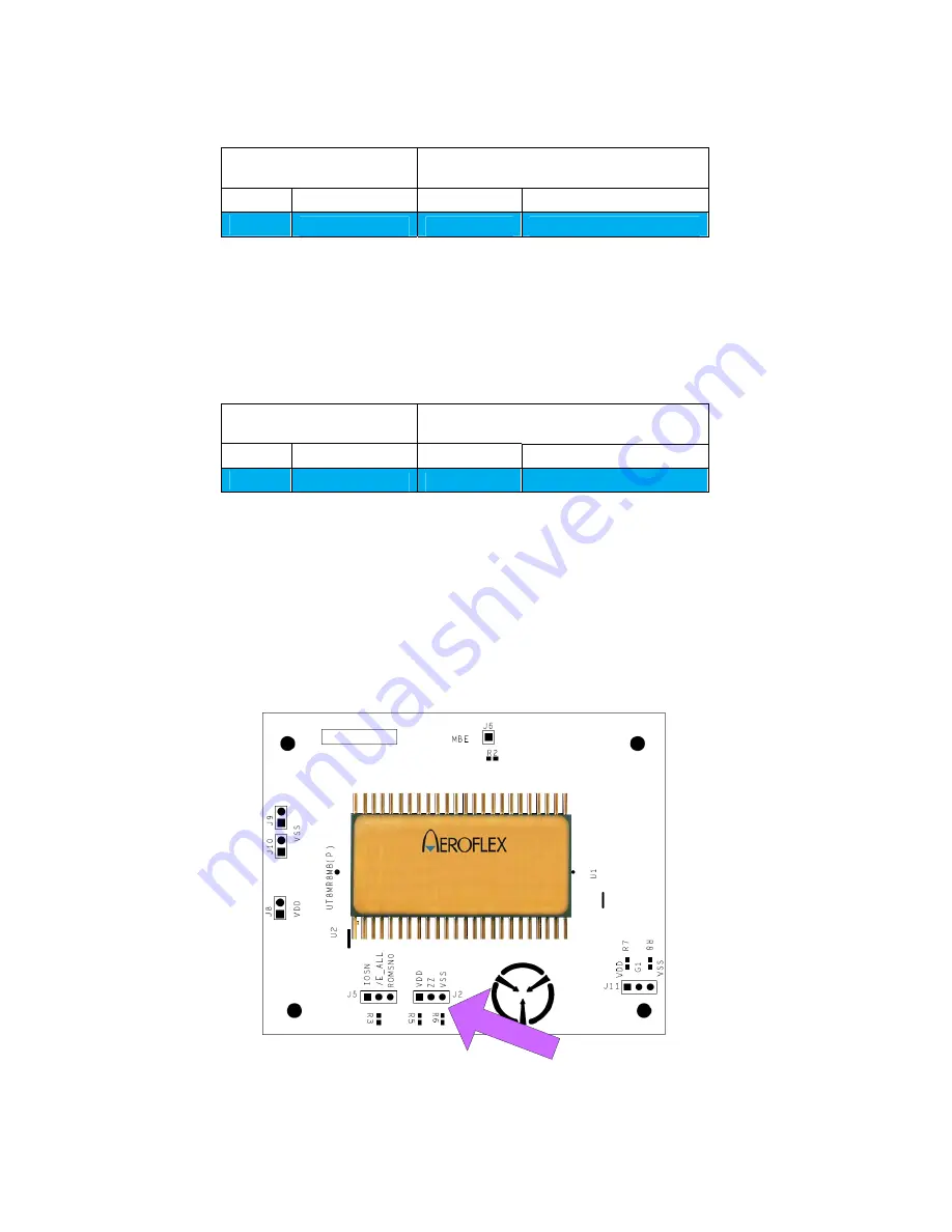
Deep Sleep Power Down (ZZ)  


ZZ controls the sleep mode operation. Enabling sleep mode causes all other inputs to be do not cares. ZZ 
places all die into internal low power even while system power is still applied to VDD.  Pin 12 on the 
UT8MR8M8 are routed to a three pin header J2.  The center pin on the three pin J2 header is tied to the ZZ 
pin, the other pins are tied to VDD and VSS.   Please refer to the UT8MR8M8 datasheet for further 
information. 


Dee

p Pow

er D

own

UT8MR8M8


Figure 7. ZZ pin 

5.8


Multi-Bit Error Flag (MBE) 

Summary of Contents for UT8MR8M8-EVB

Page 1: ...tomatically protected against power loss by a low voltage write inhibit The UT8MR8M8 EVB allows the user access to most all the features of the 64Mb MRAM via bench top evaluation or using the UT699 LE...

Page 2: ...2 4 0 FUNCTIONAL DIAGRAM UT8MR8M8 64M Non Volatile MRAM 64 Lead FP MCM Figure 1 Notional UT8MR8M8 EVB block diagram...

Page 3: ...evice Power to the board may be provided through the J9 connector on the GR UT699 CPCI Development Board or through the 100 mil connector J8 on the UT8MR8M8 EVB Only one power source should be used at...

Page 4: ...board Ensure that the mating connectors are lined up and that the power is removed from the GR cPCI UT699 eval board prior to plugging in the MRAM evaluation board Table 1 LEON 3FT EVB Power Pins J9 T...

Page 5: ...5 Figure 3 Aeroflex Gaisler LEON 3FT J7 to J9 connector...

Page 6: ...in Signal 45 A0 10 A0 76 A1 9 A1 44 A2 8 A2 77 A3 7 A3 43 A4 6 A4 78 A5 28 A5 42 A6 27 A6 79 A7 26 A7 39 A8 25 A8 82 A9 24 A9 38 A10 41 A10 83 A11 40 A11 37 A12 39 A12 84 A13 38 A13 36 A14 37 A14 85 A...

Page 7: ...inputs outputs are connected to J7 as shown in table 4 Table 4 Data I O J7 pin out LEON 3FT connector J9 UT8MR8M8 Device J7 Pin Signal Pin Signal 95 D24 46 DATA0 97 D25 47 DATA1 99 D26 50 DATA2 103 D2...

Page 8: ...l the UT8MR8M8 74 IOSN 21 Can be jumpered to E_ALL The user can exercise either the IOSN or ROMSN0 pin on the LEON 3FT to exercise the E_All pin on the MRAM There is a three pin header J5 that allows...

Page 9: ...LEON 3FT connector J9 UT8MR8M8 Device J7 Pin Signal Pin Signal 47 OEB 53 G 5 7 Deep Sleep Power Down ZZ ZZ controls the sleep mode operation Enabling sleep mode causes all other inputs to be do not c...

Page 10: ...e The following steps describe how the user to get the UT8MR8M8 EVB up and running with the UT699 LEON 3FT EVB 1 Connect J5to the UT8MR8M8 EVB to ROMSN0 for using MRAM as PROM or Connect J5to the UT8M...

Page 11: ...O1 0 8 bit Mode Closed 3 PIO2 0 PROM EDAC disabled Closed 4 PIO3 1 Open 5 PIO4 1 Open 6 PIO5 1 Open 7 PIO6 1 Open 8 PIO7 1 Open Table 9 Quick Start LEON 3FT S4 Configuration DIP Switch S4 Switch Funct...

Page 12: ...5 6 Install 7 8 Install 9 10 Install 11 12 Install 13 14 Install 15 16 Install 17 18 Install 19 20 Install PCI Host Mode Pull ups enabled see section 2 11 JP9 1 2 Install 3 4 Install PCI Host Mode se...

Page 13: ...evaluation board J9 on the GR UT699 evaluation board is pinned out as listed in table 12 below For further information on interfacing the UT8MR8M8 EVB with the GR UT699 Evaluation board please see the...

Page 14: ...A8 40 3 3V 41 VSS 42 A6 27 A6 43 A4 6 A4 44 A2 8 A2 45 A0 10 A0 46 WEB 42 WEB 47 OEB 53 OEB 48 ROMSN0 ROMSN0 49 RAMSN4 NC 50 VSS 51 3 3V 52 RAMSN3 NC 53 RAMSN2 NC 54 RAMSN1 NC 55 RAMSN0 NC 56 RWEN2 N...

Page 15: ...58 A15 86 A17 56 A17 87 A19 11 A19 88 A21 22 A21 89 A23 NC 90 VSS 91 3 3V 92 A25 NC 93 A27 NC 94 D16 NC 95 D24 46 DATA0 96 D17 NC 97 D25 47 DATA1 98 D18 NC 99 D26 50 DATA2 100 VSS 101 3 3V 102 D19 NC...

Page 16: ...16 116 VSS 117 12V NC 118 VSS 119 5V NC 120 VSS...

Page 17: ...17 8 0 BOARD SCHEMATICS The schematics are for reference ONLY...

Page 18: ...7 47uF J11 HEADER 3 1 2 3 J8 HEADER 2 1 2 C6 0 01uF C1 0 1uF J5 HEADER 3 1 2 3 R3 10k J10 HEADER 2 1 2 C4 0 01uF CONN_MEZ120 J7 DGND 1 5V 2 DGND 3 12V 4 DGND 5 12V 6 DGND 7 D15 8 D7 9 3 3V 10 DGND 11...

Page 19: ...18 ORDERING INFORMATION UT Device Type 8MR8M8 EVB 64Megabit Non Volatile MRAM Evaluation Board...

Page 20: ...19 Aeroflex Colorado Springs Datasheet Definition Advanced Datasheet Product In Development Preliminary Datasheet Shipping Prototype Datasheet Shipping QML Reduced Hi Rel...

Reviews: