100
Chapter 8: Theory of Operation
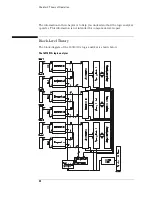
onto the card and provides for control of the card by the analyzer mainframe. It
also provides a path for unloading acquired data to the analyzer display.
The FPGA converts bus signals generated by the mainframe processor into
control signals for the logic analyzer card. It also provides centralized functions
for the card such as I2C, Calibration signals, Flag routing, and Timing mode
sample clock.
Summary of Contents for 16900 Series
Page 3: ...3 Chapter The 16910A Logic Analyzer The 16911A Logic Analyzer...
Page 8: ...8 Contents...
Page 14: ...14 Chapter 1 General Information...
Page 18: ...18 Chapter 2 Preparing for Use...
Page 61: ...61 4 Calibrating This chapter gives you instructions for calibrating the logic analyzer...
Page 65: ...65 Chapter 5 Troubleshooting Troubleshooting Flowchart 1...
Page 66: ...66 Chapter 5 Troubleshooting Troubleshooting Flowchart 2...
Page 82: ...82 Chapter 5 Troubleshooting To test the cables 18 Return to the troubleshooting flow chart...
Page 94: ...94 Chapter 7 Replaceable Parts 16910A Exploded View Exploded view of the 16910A logic analyzer...
Page 95: ...95 Chapter 7 Replaceable Parts 16911A Exploded View Exploded view of the 16911A logic analyzer...
Page 96: ...96 Chapter 7 Replaceable Parts...
Page 102: ...102 Index...


