background image

54

Chapter 2

Making Adjustments

5. Crystal and LC Bandwidth Filter

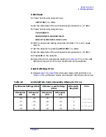
26.Adjust A13C45 LC CTR for maximum signal at center-screen.

27.Move the short from A11TP10 and A11TP11 to A11TP12 and

A11TP13, then adjust A11C23 LC CTR for maximum signal at
center-screen.

28.Move the short from A13TP12 and A13TP13 to A11TP10 and

A11TP11, then adjust A13C45 LC CTR for maximum signal at
center-screen.

29.Move the short from A13TP10 and A13TP11 to A13TP12 and

A13TP13, then adjust A13C23 LC CTR for maximum signal at
center-screen.

30.Disconnect all the shorts from A11 and A13 bandwidth board

assemblies.

LC Amplitude

31.Press the following analyzer keys.

BW

, 3,

MHz

SPAN

, 2,

MHz

32.Press

AMPLITUDE

 and adjust the signal level one division below the

top graticule using the knob.

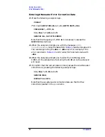
33.Press the following analyzer keys.

PEAK SEARCH

,

MARKER

 ∆

MKR FCTN

,

MK TRACK ON OFF

(ON)

BW

, 100,

kHz

It may be necessary to occasionally recenter the 30 kHz bandwidth.

34.Adjust A11R26 LC and A13R26 LC equally for a MARKER

amplitude of 0 dB. Each potentiometer should be adjusted to
accomplish one-half of the necessary increase in signal amplitude. If
A11R26 or A13R26 reaches its limit, recenter both potentiometers
and repeat

step 31

 to

step 35

.

35.Press

MKR FCTN

,

 MK TRACK ON OFF

 (OFF) on the analyzer.

Summary of Contents for 8590L

Page 1: ...ding but not limited to the implied warranties of merchantability and fitness for a particular purpose Agilent Technologies shall not be liable for errors contained herein or for incidental or consequential damages in connection with the furnishing performance or use of this material Advanced Test Equipment Rentals www atecorp com 800 404 ATEC 2832 Established 1981 ...

Page 2: ...e year from date of shipment During the warranty period Agilent Technologies will at its option either repair or replace products which prove to be defective For warranty service or repair this product must be returned to a service facility designated by Agilent Technologies Buyer shall prepay shipping charges to Agilent Technologies and Agilent Technologies shall pay shipping charges to return th...

Page 3: ...OLOGIES SPECIFICALLY DISCLAIMS THE IMPLIED WARRANTIES OF MERCHANTABILITY AND FITNESS FOR A PARTICULAR PURPOSE Exclusive Remedies THE REMEDIES PROVIDED HEREIN ARE BUYER S SOLE AND EXCLUSIVE REMEDIES AGILENT TECHNOLOGIES SHALL NOT BE LIABLE FOR ANY DIRECT INDIRECT SPECIAL INCIDENTAL OR CONSEQUENTIAL DAMAGES WHETHER BASED ON CONTRACT TORT OR ANY OTHER LEGAL THEORY Assistance Product maintenance agree...

Page 4: ... your analyzer to determine if the analyzer meets its specifications 8590 E Series and L Series Spectrum Analyzers User s Guide Tells you how to make measurements with your analyzer Describes the analyzer features Tells you what to do in case of a failure 8590 E Series and L Series Spectrum Analyzers Quick Reference Guide Describes how to make a simple measurement with your analyzer Briefly descri...

Page 5: ...ou how to make measurements using the spectrum analyzer mode Describes the spectrum analyzer mode features Tells you what to do in case of a failure 8591C Cable TV Analyzer Getting Started and Quick Reference Guide Describes how to make a simple measurement with your analyzer Briefly describes the cable TV and spectrum analyzer functions Provides a quick reference for cable TV and spectrum analyze...

Page 6: ...0 195 DVB C Data Measurements Tells you how to make QAM measurements with your analyzer Describes the QAM analyzer mode features Spectrum Analyzer Reference Tells you how to make measurements using the spectrum analyzer mode Describes the spectrum analyzer mode features Tells you what to do in case of a failure 8594Q Option 190 195 DVB C Data Measurement QAM Analyzer Getting Started and Quick Refe...

Page 7: ...two manuals 8590 Series Analyzers Assembly Level Repair Service Guide Describes adjustment and assembly level repair of the analyzer 8590 Series Analyzers Component Level Repair Service Guide Provides information for component level repair of the analyzer How to Order Guides Each of the guides listed above can be ordered individually To order contact your local Sales and Service Office How to Use ...

Page 8: ...d Linear Amplifier 63 8 CAL FREQ Adjustment Routine 68 9 CAL AMPTD Adjustment Routine 70 10 CAL YTF Adjustment Routine 72 11 CAL MXR Adjustment Routine 77 12 Second Converter 79 13 Third Converter and Second IF Bandpass 85 14 Comb Generator 92 15 Frequency Response of the 8590L 8591C and 8591E 96 16 Frequency Response of the 8592L 94L 8593E 94E 95E 96E and 8594Q 106 17 Time and Date 124 18 Modulat...

Page 9: ...deo Problem 232 Using the Internal Service Diagnostic Routines 238 Troubleshooting the A16 Processor Video Board Assembly 249 5 Troubleshooting the IF Section Before You Start 254 Service Equipment You Will Need 254 After an Analyzer Repair 255 IF Section Information 255 IF Power Level Measurement 256 Troubleshooting the A15 Motherboard Assembly 266 6 Troubleshooting the RF Section Before You Star...

Page 10: ...58 RF and LO Section for 8590L 8591E and 8591C Spectrum Analyzers 359 RF and LO Section for 8592L 8593E 8594E 8594L 8594Q 8595E and 8596E Analyzers 365 IF Section 373 10 Analyzer Options and Block Diagrams Analyzer Options and Block Diagrams 394 Option Descriptions 397 Troubleshooting Analyzer Options 408 Tracking Generator 8593E 8594E 8595E 8596E Option 010 410 First LO Distribution Amplifier LOD...

Page 11: ...essages 614 15 Service Equipment and Tools Service Equipment and Tools 660 16 Safety and Regulatory Information Safety Considerations 668 Safety Symbols 668 Instrument Markings 669 General Safety Considerations 670 Protection from Electrostatic Discharge 672 ...

Page 12: ...Series Analyzers Assembly Level Repair Service Guide provides the information needed to adjust and repair the 8590 E Series and L Series spectrum analyzers the 8591C cable TV analyzer and 8594Q QAM analyzer to the assembly level ...

Page 13: ...r selected assemblies Each CLIP contains component level schematics a component parts list and illustrations for component location by reference designator Each CLIP has its own part number which is changed whenever the part number for its related analyzer assembly is changed A list of all CLIP part numbers for the 8590 E Series and L Series spectrum analyzers 8591C cable TV analyzers and 8594Q QA...

Page 14: ...on for selected assemblies in the IF section and the A15 Motherland assembly Chapter 6 Troubleshooting the RF Section contains troubleshooting information for the RF and LO sections of the 8590 E Series and L Series spectrum analyzer and 8591C cable TV analyzer The information is separated by the following tabs Chapter 6a 8590L 8591C and 8591E contains specific troubleshooting information for sele...

Page 15: ...d Microwave frequency ranges The frequency ranges of 8590 E Series and L Series spectrum analyzers 8591C cable TV analyzers and 8594Q QAM analyzers are described below All 8590 E Series spectrum analyzers 8591C cable TV analyzers and 8594Q QAM analyzers are equipped with a memory card reader The memory card reader allows the analyzer to use downloadable software programs The functional personality...

Page 16: ...Frequency Ranges Analyzer Model Frequency Range 8590L 9 kHz to 1 8 GHz 8591E 9 kHz to 1 8 GHz 8591C 1 MHz to 1 8 GHz 8592L 9 kHz to 22 0 GHz 8592L Option 026 9 kHz to 26 5 GHz 8593E 9 kHz to 22 0 GHz 8593E Option 026 9 kHz to 26 5 GHz 8594E 9 kHz to 2 9 GHz 8594L 9 kHz to 2 9 GHz 8594Q 9 kHz to 2 9 GHz 8595E 9 kHz to 6 5 GHz 8596E 9 kHz to 12 8 GHz ...

Page 17: ...rmware date along with the complete serial number and option designation This will ensure that you obtain accurate service information Firmware Upgrade Kit Ordering Information There are occasions when the factory revises the analyzer firmware to correct defects or make performance improvements When a firmware revision is needed a service note is distributed by the factory to all Agilent Technolog...

Page 18: ...y to protect its input circuitry The analyzer input can easily be protected by disconnecting it from the signal source whenever it is likely that large transients will be present When it is impractical to disconnect the analyzer a transient limiting device should be used The 11947A Transient Limiter is an analyzer accessory that protects the input circuitry from transients and accidental overloads...

Page 19: ... V rms input attenuation 10 dB 50 dBm 100 W for 10 µs pulse width and 1 duty cycle ssfs input attenuation 30 dB dc 0 Vdc Table 1 4 8594E and 8594L Spectrum Analyzer and 8594Q Analyzer Maximum Safe Input Level INPUT 50Ω Input Attenuation 10 dB Average Continuous Power Peak Pulse Power 30 dBm 1 W 7 1 V rms 50 dBm 100 W for 10 µs pulse width and 1 duty cycle input attenuation 30 dB dc 0 V dc coupled ...

Page 20: ...alyzer Adjustment Procedures Adjustment for Spectrum Analyzer Model Adjustment Procedure Name 8590L 8591C 8591E 8592L 8593E 8596E 8594E 8594L 8594Q 8595E 1 Display 2 Sampler Match 3 10 MHz Reference 4 10 MHz Precision Frequency Reference 5 Crystal and LC Bandwidth Filter 6 Cal Attenuator Errora 6a Cal Attenuator Errorb 7 Log and Linear Amplifiera 7a Log and Linear Amplifierb 8 CAL FREQ Adjustment ...

Page 21: ...the Absolute Amplitude Accuracy for Option 050 26 Correcting for Absolute Amplitude Accuracy for Option 050 27 Checking the Absolute Amplitude Accuracy for Option 051 28 Correcting for Absolute Amplitude Accuracy for Option 051 a If a 3335A source is not available use the alternative adjustment with the same number found in Chapter 2a Making Adjustments If 3335A Source Not Avail able b If a 3335A ...

Page 22: ... test equipment accessories and adapters When A 3335A Source Is Not Available The 3335A Synthesizer Level Generator signal source has become obsolete because parts used in the manufacture of this instrument are no longer available from suppliers To meet the need of our customers this service guide has been revised to add new adjustments that do not use the 3335A Synthesizer Level Generator This re...

Page 23: ... operation Under most conditions of use you should test the analyzer at least once a year with either operation verification or the complete set of performance verification tests located in the calibration guide for your instrument When test results show proper operation and calibration no adjustments are necessary However if test results indicate that the instrument does not meet specifications t...

Page 24: ...Repaired Assemblies Replaced or Repaired Assembly Related Adjustments and Adjustment Routines Related Performance Verification Tests A1 Front Frame CAL AMPTD Frequency Response Residual Responses A2 Display Display CAL AMPTD Frequency Response Residual Responses A3A1 Comb Generator Comb Generator CAL YTF Comb Generator Frequency Accuracy Frequency Response Residual Responses A3A2 Microwave Switch ...

Page 25: ... CAL FREQ CAL AMPTD CAL YTF CAL MXR Frequency Response Noise Sidebands System Related Sidebands Frequency Response Other Input Related Spurious Responses Spurious Response Displayed Average Noise Residual Responses A3A9 Bandpass Filter CAL FREQ CAL AMPTD None A3A10 Directional Coupler CAL FREQ CAL AMPTD CAL YTF System Related Sidebands Frequency Response Other Input Related Spurious Responses Spur...

Page 26: ...ed Spurious Responses Spurious Response Residual Responses A3 Input Attenuator CAL FREQ CAL AMPTD Frequency Response A4 First Converter Frequency Response CAL FREQ CAL AMPTD Noise Sidebands System Related Sidebands Frequency Response Spurious Response Gain Compression Displayed Average Noise Residual Responses A5 Second Converter Second Converter CAL FREQ CAL AMPTD Noise Sidebands Residual FM Syst...

Page 27: ...Level Flatness Harmonic Spurious Outputs Non Harmonic Spurious Outputs Tracking Generator Feedthrough A8 Power Supply None System Related Sidebands Spurious Responses Residual Responses A9 Third Converter Third Converter Second IF Bandpass CAL FREQ CAL AMPTD BITG Power Level for Option 010 only Noise Sidebands System Related Sidebands Absolute Amplitude Calibration and Resolution Bandwidth Switchi...

Page 28: ...e Fidelity Reference Level Accuracy A15 Motherboard CAL FREQ CAL AMPTD Complete Operation Verification A16 Processor Video A16A1 Memory 10 MHz Reference CAL FREQ CAL AMPTD CAL YTF 8592L 8593E 8595E 8596E only CAL MXR 8592L 8593E 8595E 8596E only Cal Attenuator Error Frequency Response Time and Date Reference Level Accuracy Frequency Response These adjustments are not necessary if valid correction ...

Page 29: ...30 Chapter1 Introduction If You Replace or Repair an Assembly ...

Page 30: ...trical performance to the specifications described in Chapter 2 of the calibration guide for your instrument Most adjustments require access to the interior of the analyzer If a 3335A source is not available use the alternative adjustments with the same number found in Chapter 2a ...

Page 31: ... on the analyzer and read the general safety considerations and the symbol definitions given in the front of this service guide Check that the analyzer has been turned on and allowed to warm up for at least 30 minutes at room temperature before making any adjustments The analyzer must be allowed to stand at room temperature at least 2 hours prior to the 30 minute warmup Read the rest of this secti...

Page 32: ...here are two focus adjustments fine and coarse The fine adjustment is located on the left side of the display assembly and can be accessed with the instrument cover on or off The coarse adjustment is located on the rear of the display assembly and can only be adjusted with the instrument cover off Procedure Display Position 1 Press the following analyzer keys to adjust the horizontal position PRES...

Page 33: ...ENSITY control for a comfortable viewing intensity 2 Use an adjustment tool to access the fine focus adjustment See Figure 2 1 Adjust as necessary for a focused display If one of the end stops of the fine focus adjustment is reached proceed with the Coarse Focus Adjustment section Figure 2 1 Fine Focus Adjustment Location ...

Page 34: ...ING The analyzer contains potentially hazardous voltages Refer to the safety symbols provided on the analyzer and in the general safety instructions in this guide before operating the unit with the cover removed Ensure that safety instructions are strictly followed Failure to do so can result in severe or fatal injury 3 Turn the analyzer LINE switch to ON 4 Center the fine focus adjustment Refer t...

Page 35: ...es in the top of the shield continue with this procedure If it has four holes go to the preceding procedure If you are going to make adjustments to your display only make the adjustments that would correct the problem that the display is experiencing The following is a list of adjustments described in this procedure The horizontal and vertical display positions should first be adjusted using front...

Page 36: ...2 of 3 DEFAULT SYNC CAL More 1 of 4 More 2 of 4 DEFAULT CAL DATA Focus The Focus potentiometer is located on the left side of the instrument and can be accessed with the instrument cover on or off Use the specified adjustment tool to make this adjustment 1 Adjust the front panel INTENSITY control for a comfortable viewing intensity 2 Adjust as necessary for a focused display See Figure 2 1 Figure ...

Page 37: ...f the display s cover The instrument cover must be removed for access to the display s cover Refer to Figure 2 4 for the location of this adjustment Use the specified adjustment tool to make this adjustment 1 Press CAL More 1 of 4 CRT HORZ POSITION 2 Set the CRT horizontal position setting to 12 3 Set the Centering potentiometer so the displayed image is positioned approximately at the center of t...

Page 38: ...splay begins to roll horizontally 5 Find the counter clockwise position of the Horizontal Hold potentiometer where the display begins to roll horizontally 6 Set the adjustment to a position approximately midway between the clockwise and counter clockwise position where the display does not roll horizontally Vertical Hold Perform this adjustment only if the displayed image is rolling vertically on ...

Page 39: ... Press CAL More 1 of 4 CRT VERT POSITION 2 Set the CRT vertical position setting so that softkey labels are adjacent to the keys at the right to which they are associated 3 Adjust the Vertical Size potentiometer so that the uppermost softkey label is adjacent to the uppermost softkey and the lowermost softkey label is adjacent to the lowermost softkey 4 Repeat step 2 and step 3 if necessary Vertic...

Page 40: ...he Contrast potentiometer to the full clockwise position the image is no longer displayed 2 Adjust the front panel INTEN knob to the full clockwise position 3 Adjust the Bright potentiometer until the background is just barely extinguished the background is dark 4 Adjust the front panel INTEN knob to the full counter clockwise position 5 Adjust the Contrast potentiometer until the image is just ba...

Page 41: ...E switch to OFF Remove the instrument over assembly 2 Turn the analyzer LINE switch to ON 3 Set the center frequency of the analyzer to 194 MHz If you are adjusting an 8590L or 8591E spectrum analyzer or an 8591C cable TV analyzer set the center frequency to 265 MHz 4 Press the following analyzer keys SPAN 10 MHz 5 Connect the digital multimeter DMM from chassis ground to A25TP1 Refer to Figure 2 ...

Page 42: ...Chapter 2 43 Making Adjustments 2 Sampler Match Figure 2 5 A25 Counter Lock Assembly Test Points ...

Page 43: ...quency accuracy This procedure does not adjust for long term drift or aging rate Only short term accuracy is adjusted A frequency counter is connected to the CAL OUT which is locked to the 10 MHz reference This yields better effective resolution The time base is adjusted for a frequency of 300 MHz as read by the frequency counter Equipment Required Microwave frequency counter Frequency standard Ca...

Page 44: ...e FREQUENCY STANDARD EXTERNAL 3 Press the following analyzer keys PRESET FREQUENCY 2001 Hz CAL More 1 of 4 More 2 of 4 More 3 of 4 SERVICE CAL CAL TIMEBASE 4 A number will be displayed in the active function block of the analyzer display This is the setting of the DAC 0 to 255 which controls the frequency of the internal time base Use the knob or keyboard to change the DAC setting until the freque...

Page 45: ...Failure to allow sufficient stabilization time could result in the misadjustment of the oscillator The frequency of the internal 10 MHz frequency reference is compared to a known frequency standard and adjusted for minimum frequency error This procedure does not adjust the short term stability or long term stability of the 10 MHz Ovenized Crystal Oscillator OCXO which are determined by characteris...

Page 46: ...equency counter 5 Set the frequency counter controls as follows FUNCTION DATA FREQ A INPUT A x10 ATTN OFF AC OFF DC coupled 50 Ω Z OFF 1 MΩ input impedance AUTO TRIG ON 100 kHz FILTER A OFF INT EXT switch rear panel EXT 6 On the frequency counter select a 1 second gate time and a 10 MHz offset of the displayed frequency by pressing the following frequency counter keys GATE TIME 1 GATE TIME MATH SE...

Page 47: ...er should now display the difference between the frequency of the INPUT A signal and 10 0 MHz with a resolution of 0 001 Hz 1 MHz 10 Wait at least 2 gate periods for the frequency counter to settle and then adjust the FREQ ADJ control on the OCXO for a stable frequency counter indication of 0 000 0 010 Hz 11 Replace the dust cap screw on the OCXO Figure 2 8 Oven Reference Adjustment Location ...

Page 48: ... constants are turned off This allows for uncorrected 3 dB resolution bandwidth centering and amplitude adjustments New corrections are then generated by performing the CAL FREQ and CAL AMPTD adjustment routines Equipment Required Crystal shorts set of three Cable BNC 23 cm 9 in Additional Equipment for 75 Ω Input Cable BNC 75 Ω 30 cm 12 in Procedure 1 Turn the analyzer LINE switch to OFF Remove t...

Page 49: ...igure 2 9 Crystal Symmetry and Centering CAUTION Use only 75 Ω cables connectors or adapters on instruments equipped with 75 Ω inputs or damage to the input connectors will occur 4 Press the following analyzer keys FREQUENCY 300 MHz SPAN 10 MHz PEAK SEARCH MKR FCTN MK TRACK ON OFF ON 75 Ω input AMPLITUDE More 1 of 2 AMPTD UNITS dBm SPAN 200 kHz AMPLITUDE 20 dBm SCALE LOG LIN LIN More 1 of 2 AMPTD ...

Page 50: ...litude Then adjust A13C38 SYM and A13C54 CTR for a centered and symmetrical bandpass response as shown in Figure 2 9 9 Remove the crystal short from A13TP1 and A13TP2 and connect it across A13TP4 and A13TP5 10 Adjust A13C25 CTR for minimum signal amplitude Then adjust A13C15 SYM and A13C25 CTR for a centered and symmetrical bandpass response 11 Remove the crystal short from A11TP4 and A11TP5 Conne...

Page 51: ...r keys PEAK SEARCH MKR FCTN MK TRACK ON OFF ON SPAN 50 kHz MKR FCTN MK TRACK ON OFF OFF BW 3 kHz PEAK SEARCH MARKER DELTA BW 30 kHz PEAK SEARCH 16 Verify that the MARKER frequency does not exceed 3 kHz If the signal shift is out of tolerance repeat step 3 to step 16 17 Press the following analyzer keys MKR MARKER 1 ON OFF OFF ...

Page 52: ...Move the short from A13TP10 and A13TP11 to A13TP12 and A13TP13 then adjust A13C17 LC dip for a minimum signal amplitude 23 Move the short from A11TP10 and A11TP11 to A13TP10 and A13TP11 then adjust A11C17 LC dip for a minimum signal amplitude 24 Move the short from A11TP12 and A11TP13 to A11TP10 and A11TP11 then adjust A11C47 LC dip for a minimum signal amplitude LC Centering Note that the center ...

Page 53: ...ct all the shorts from A11 and A13 bandwidth board assemblies LC Amplitude 31 Press the following analyzer keys BW 3 MHz SPAN 2 MHz 32 Press AMPLITUDE and adjust the signal level one division below the top graticule using the knob 33 Press the following analyzer keys PEAK SEARCH MARKER MKR FCTN MK TRACK ON OFF ON BW 100 kHz It may be necessary to occasionally recenter the 30 kHz bandwidth 34 Adjus...

Page 54: ...ess the following analyzer keys BW 30 kHz PEAK SEARCH MARKER BW 100 kHz PEAK SEARCH 40 Verify that the MARKER frequency does not exceed 10 kHz If the signal shift is out of tolerance repeat step 26 to step 39 Crystal Amplitude 41 Press the following analyzer keys BW 30 kHz SPAN 10 kHz PEAK SEARCH MARKER MKR FCTN MK TRACK ON OFF ON BW 1 kHz 42 Adjust A11R31 XTL and A13R31 XTL equally for a MARKER a...

Page 55: ... example of the XTAL and LC bandwidth amplitude correction numbers that will be displayed on the analyzer Perform the following steps that apply to your analyzer If the difference between the bandwidth amplitude correction numbers of the 30 kHz XTAL and 3 MHz LC is greater than 0 8 dB pad A11R8 or A13R8 and repeat the Final BW Amplitude Check Refer to the Component Level Information Package for th...

Page 56: ...idth Amplitude Correction Map Resolution Bandwidths BW AMP Correction Numbers not used 0 00 not used 0 00 not used 0 00 not used 0 00 XTAL 9 kHz 0 00 300 Hz 0 46 1 kHz 0 06 3 kHz 0 02 10 kHz 0 00 30 kHz 0 00 LC 100 kHz 0 27 300 kHz 0 40 1 MHz 0 43 3 MHz 0 47 5 MHz 0 54 120 kHz 0 17 ...

Page 57: ...8 dB and 16 dB attenuators which are correctable The 16 dB step is not used at this time The attenuator error correction procedure involves disabling the attenuator correction constants determining the attenuator step errors and entering the new correction constants into the analyzer memory Equipment Required Synthesizer level generator Cable BNC 120 cm 48 in Adapter Type N m to BNC f Additional E...

Page 58: ...he synthesizer level generator to the analyzer INPUT 50 Ω See Figure 2 10 75 Ω input Connect the 75 Ω output of the synthesizer level generator to the analyzer INPUT 75 Ω Figure 2 10 Cal Attenuator Error Correction Setup CAUTION Use only 75 Ω cables connectors or adapters on instruments equipped with 75 Ω inputs or damage to the input connectors will occur 4 Set the frequency of the synthesizer le...

Page 59: ...TN MK TRACK ON OFF ON SPAN 50 kHz BW 3 kHz VID BW AUTO MAN 300 Hz 7 Press the following analyzer keys PEAK SEARCH MARKER DELTA MKR FCTN MK TRACK ON OFF ON 8 The MKR amplitude reading should be 0 0 dB 0 01 dB If it is not repeat step 7 9 Set the analyzer by pressing AMPLITUDE 17 dBm 10 Set the amplitude of the synthesizer level generator to 18 dBm 11 Press MKR on the analyzer 12 Record the MKR ampl...

Page 60: ...zer level generator to 15 dBm 19 Press MKR on the analyzer 20 Record the MKR amplitude reading in Table 2 2 This is the 2 dB attenuator step error of the A12 amplitude control assembly 4 and 8 dB Step Error 21 Repeat step 13 to step 20 for attenuator steps 4 dB and 8 dB Use Table 2 2 for synthesizer values and analyzer reference level values Table 2 2 A12 Amplitude Control Assembly Attenuator Erro...

Page 61: ...N ERROR enter the data from Table 2 2 and terminate with the reverse sign using the dBm or dBm keys For example if the error recorded in Table 2 2 is 0 07 enter 0 07 and terminate with dBm 24 When the analyzer prompts you to enter the 16 dB step enter 0 dBm At the completion of entering the 16 dB error the analyzer will reset 25 To confirm that the correct data is stored access the cal attenuator ...

Page 62: ...Hz signal is injected into an IF test board that has been inserted in place of the first resolution bandwidth assembly A11 The gain of the A14 log amplifier assembly is adjusted by observing the voltage at the AUX VIDEO OUT on the rear panel with a digital multimeter Equipment Required Synthesizer level generator Digital multimeter DMM IF test board Cable BNC 120 cm 48 in Cable BNC f to dual banan...

Page 63: ... DMM to read dc volts 4 Press the following analyzer keys PRESET CAL More 1 of 4 CORRECT ON OFF OFF More 2 of 4 SERVICE DIAG STP GAIN ZERO SPAN 0 Hz BW 10 kHz VID BW AUTO MAN 300 Hz AMPLITUDE 10 dBm SCALE LOG LIN LIN 5 Set the synthesizer as follows FREQUENCY 21 4 MHz MANUAL TUNE ON AMPTD INCR 0 01 dBm AMPLITUDE 6 dBm 6 Connect equipment as shown in Figure 2 11 Connect the output of the synthesize...

Page 64: ...zer amplitude as necessary to keep the signal on the display 8 Adjust the synthesizer output level for a DMM reading of 1000 mV 1 0 mV Record the synthesizer amplitude readout for later reference ____________________dBm 9 Press AMPTD INCR 10 dB on the synthesizer 10 Press SCALE LOG on the analyzer 11 Set the synthesizer to the level recorded in step 8 and adjust A14R23 SLOPE refer to Figure 2 12 f...

Page 65: ...adjust the A14R23 SLOPE for a DMM reading of 625 mV 1 mV 15 Set the synthesizer amplitude to the level recorded in step 8 and adjust the A14R69 30 dB for a DMM reading of 1000 mV 1 mV 16 Repeat step 13 and step 14 until no further adjustment is necessary 17 Set the synthesizer amplitude 10 dB below that recorded in step 8 and adjust the A14R23 SLOPE for a DMM reading of 875 mV 1 mV 18 Set the synt...

Page 66: ...ble 2 3 Log Fidelity Check Synthesizer Level DMM Reading Reference from step 8 1000 mV 1 mV Reference 10 dB 875 mV 3 mV Reference 20 dB 750 mV 4 mV Reference 30 dB 625 mV 4 mV Reference 40 dB 500 mV 5 mV Reference 50 dB 375 mV 6 mV Reference 60 dB 250 mV 7 mV Reference 70 dB 125 mV 8 mV Table 2 4 Linear Gain Check Adjust Synthesizer Level Reference Level dBm DMM Reading A14R34 Reference from step ...

Page 67: ...e CAL FREQ Adjustment Routine adjusts the analyzer to obtain frequency accuracy using CAL OUT signal The following adjustments are automatically performed by CAL FREQ routine Sweeptime calibration YTO offset and slope FM coil timing constants Span attenuator FM detector sensitivity Equipment Required Cable BNC 20 cm 9 in Adapter Type N m to BNC f Additional Equipment for Option 026 Adapter Type AP...

Page 68: ...tup CAUTION Use only 75 Ω cables connectors or adapters on instruments equipped with 75 Ω inputs or damage to the input connectors will occur 2 Press the following analyzer keys CAL CAL FREQ The CAL FREQ adjustment routine will take a few minutes to run The internal adjustment data will be stored in working RAM To store this data in nonvolatile memory press CAL STORE If the CAL AMPTD adjustment ro...

Page 69: ...usting the gain of the IF section The 3 dB resolution bandwidths are adjusted Bandwidth amplitude errors are determined Errors are corrected with video offsets Step gain and input attenuator errors are determined Errors are corrected with video offsets Log fidelity is checked in 1 dB steps Errors are corrected with video offsets Frequency accuracy is tested and adjusted by using frequency offsets ...

Page 70: ...onnect the CAL OUT to the INPUT 75 Ω with the 75 Ω BNC cable Figure 2 14 CAL AMPTD Adjustment Routine Setup CAUTION Use only 75 Ω cables connectors or adapters on instruments equipped with 75 Ω inputs or damage to the input connectors will occur 2 Press the following analyzer keys CAL CAL AMPTD The CAL AMPTD routine takes approximately 5 to 7 minutes to run The internal adjustment data will be sto...

Page 71: ...oftkey accesses an internal adjustment routine This routine adjusts the slope and offset of the A3A8 YTF tune voltage for each harmonic mixing band The CAL FREQ Adjustment Routine must be performed prior to this adjustment Equipment Required Cable Type N m to SMA m part number 8120 5148 Additional Equipment for Option 026 Cable SMA m to m Adapter Type APC 3 5 f to APC 3 5 f Additional Equipment fo...

Page 72: ...e CAL DONE will be displayed when the routine has finished The internal adjustment data will be stored in working RAM If the message LOST COMB SIGNAL is displayed perform the Mixer Bias DAC Initialization procedure 4 Press CAL STORE to store the YTF correction data in nonvolatile memory Mixer Bias DAC Initialization If the message LOST COMB SIGNAL is displayed the current mixer bias DAC settings m...

Page 73: ...in Table 2 5 complete the rest of this procedure to initialize the mixer bias DAC values 4 Press the following keys to allow entry of the default mixer bias DAC values PRESET FREQUENCY 2001 Hz DISPLAY CHANGE TITLE 5 Enter CALMXRDATA 1600 1 as a title entry to set the mixer bias value to 1600 for band 1 6 Press the following keys to store the mixer bias value for band 1 in nonvolatile memory CAL Mo...

Page 74: ...ERVICE CAL EXECUTE TITLE 9 Press the following keys to allow entry of the default mixer bias DAC value for band 3 DISPLAY CHANGE TITLE CLEAR 10 Enter CALMXRDATA 1300 3 as a title entry to set the mixer bias value to 1300 for band 3 11 Press the following keys to store the mixer bias value for band 3 in nonvolatile memory CAL More 1 of 4 More 2 of 4 SERVICE CAL EXECUTE TITLE 12 Press the following ...

Page 75: ...f 4 More 2 of 4 SERVICE CAL EXECUTE TITLE 15 Press the following keys to check the default mixer bias DAC values PRESET CAL More 1 of 4 More 2 of 4 SERVICE DIAG DISPLAY CAL DATA Confirm that the Optimum Bias DAC values displayed for band 1 through band 4 are 1600 20 1300 and 520 16 Repeat the CAL YTF adjustment procedure 17 Perform the CAL MXR adjustment procedure ...

Page 76: ...adjustment routine which optimizes the dc bias for the A3A6 Dual Band Mixer when in high band 2 75 to 22 GHz The CAL YTF routine must be performed prior to this adjustment New frequency response correction constants must be developed following the CAL MXR Adjustment Routine Equipment Required Cable Type N m to SMA m Additional Equipment for Option 026 Cable CAL Comb Adapter Type APC 3 5 f to APC 3...

Page 77: ...to the INPUT 50 Ω using a BNC cable Figure 2 16 CAL MXR Adjustment Setup 3 Press the following analyzer keys PRESET FREQUENCY 2001 Hz CAL More 1 of 4 More 2 of 4 SERVICE CAL CAL MXR Note that the frequency of 2001 Hz is necessary to access the SERVICE CAL routines The CAL MXR routine will take a few minutes to run The message CAL DONE will be displayed when the routine has finished The internal ad...

Page 78: ...and adjusting the slug tuned cavity for maximum signal The second IF bandpass filter is adjusted for a 2 1214 GHz bandpass using the Dishal method The second mixer match is adjusted for maximum output The LO is swept through the range of the 2 1214 GHz bandpass while the output is observed with an analyzer and the characteristics are evaluated Equipment Required Microwave spectrum analyzer Tuning ...

Page 79: ...ENTER FREQUENCY 1 8 GHz FREQUENCY SPAN 10 MHz REFERENCE LEVEL 20 dBm dB DIV 2 dB DIV 4 Connect the microwave spectrum analyzer to the 2ND LO 1 8 GHz port on the A5 Second Converter using SMB adapters and the test cable See Figure 2 17 Figure 2 17 Tripler Adjustment Setup 5 Use the tuning tool to adjust A5C4 FREQUENCY TRIPLER see Figure 2 18 for maximum signal amplitude as observed on the analyzer ...

Page 80: ...ing these lock nuts Figure 2 18 Second Converter Adjustment Location Second Converter Bandpass 6 Set the microwave spectrum analyzer controls as follows CENTER FREQUENCY 2 1214 GHz FREQUENCY SPAN 5 MHz REFERENCE LEVEL 30 dBm 7 Connect the microwave spectrum analyzer to the BP ALIGN port on the A5 Second Converter of the analyzer using the test cable See Figure 2 17 Figure 2 19 Second Converter Ban...

Page 81: ... of the cavity Do not force the tuning screws down 11 Turn A5C1 counterclockwise for a peaked signal on the 8566A B Lightly tighten the lock nut 12 Turn A5C2 counterclockwise for a minimum signal on the analyzer Lightly tighten the lock nut 13 Turn A5C3 counterclockwise for peak signal on the analyzer Lightly tighten the lock nut 14 Repeat step 11 to step 13 until no further improvement is noticea...

Page 82: ...mplitude as displayed on the microwave spectrum analyzer Adjust the reference level as necessary to keep the signal near top screen Swept Bandpass Check 18 Set the analyzer controls as follows SPAN 20 MHz SWEEP 20 SEC 19 On the microwave spectrum analyzer press trace B and MAX HOLD Wait for at least one complete sweep Then press the following keys to measure the 3 dB bandwidth TRACE B VIEW A B PEA...

Page 83: ...ise so that the marker delta amplitude reads 0 dB and is on the right hand side of the response Read the marker delta frequency it should be 15 MHz 2 5 MHz See Figure 2 21 22 The maximum ripple should be less than 1 dB for a bandwidth of 6 MHz Figure 2 21 Second Converter Bandpass Ripple Measurement ...

Page 84: ... 10 dB attenuator are characterized The harmonics of the CAL OUT signal are suppressed with the LPF before the amplitude accuracy is measured using a power meter Equipment Required Synthesized sweeper Microwave spectrum analyzer Measuring receiver used as a power meter Power meter Low power sensor with a 50 MHz reference attenuator Power sensor 300 MHz Power splitter Attenuator 10 dB Type N m to f...

Page 85: ...MENT PRESET on the microwave spectrum analyzer then set the controls as follows CENTER FREQUENCY 21 4 MHz FREQUENCY SPAN 50 MHz REFERENCE LEVEL 30 dBm dB DIV 1 dB DIV 2 Set the synthesized sweeper controls as follows CW 321 4 MHz POWER LEVEL 26 dBm 3 Turn the analyzer LINE switch to OFF Remove the instrument cover assembly 4 Remove the first IF bandwidth filter assembly A11 5 Install the IF test b...

Page 86: ...47 for maximum signal amplitude as observed on the microwave spectrum analyzer Adjust the reference level of the microwave spectrum analyzer as necessary to display the signal below the top graticule 12 Remove the test board from the A11 slot and install the A11 bandwidth filter assembly 13 Reconnect W9 to A9J4 321 4 MHz INPUT If you are adjusting an 8590L Option 713 continue with the 600 MHz Adju...

Page 87: ...ect W8 18 Continue with LPF Attenuator and Adapter Insertion Loss Characterization LPF Attenuator and Adapter Insertion Loss Characterization 19 Zero and calibrate the measuring receiver and power sensor combination in LOG mode as described in the measuring receiver operation manual CAUTION Do not attempt to calibrate the power sensor without the reference attenuator or damage to the power sensor ...

Page 88: ...ss RATIO mode Power indication should be 0 dB 24 On the power meter press the dB REF mode key Power indication should be 0 dB 25 Connect the LPF Attenuator and adapters as shown in Figure 2 23 26 Record the measuring receiver reading in dB This is the relative error due to mismatch Mismatch Error____________________dB 27 Record the power meter reading in dB This is the relative uncorrected inserti...

Page 89: ...tor Amplitude Adjustment 29 Connect the equipment as shown in Figure 2 24 The analyzer should be positioned so that the setup of the adapters LPF and attenuator do not bind It may be necessary to support the center of gravity of the devices Figure 2 24 300 MHz Calibrator Amplitude Accuracy Test Setup 30 On the power meter press the dBm mode key Record the power meter reading in dBm Power Meter Rea...

Page 90: ...For example if the Corrected Insertion Loss is 10 0 dBm and the measuring receiver reading is 30 dBm then 30 dBm 10 0 dBm 20 dBm CAL OUT Power____________________dBm 32 Adjust A9R19 CAL OUT ADJ accordingly if the CAL OUT amplitude is not 20 dBm 0 4 dB as calculated in step 26 ...

Page 91: ...000 MHz 0 0004 MHz A3A1L3 is selected to bring the frequency within tolerance The comb generator signal is adjusted for maximum output power as measured with a measuring receiver used as a power meter If the amplitude is not 26 0 0 8 dBm A3A1R6 is selected to bring the amplitude within tolerance A3A1C5 FREQ is adjusted for a comb generator frequency of 100 000000 MHz 0 000010 MHz tolerance of 10 H...

Page 92: ...Refer to the Front End Assembly removal procedure 3 Remove the A3A1 comb generator assembly from the front end assembly and place in a service position leaving W13 connected to the A7 Analog Interface 4 Remove W24 from the A3A1J1 comb generator output connector Connect the SMA cable to A3A1J1 Refer to Figure 2 25 5 Turn the analyzer LINE switch to ON 6 Press the following analyzer keys AUX CTRL CO...

Page 93: ...scilloscope display 11 Reconnect the BNC cable through the 20 dB attenuator to the frequency counter input The comb generator frequency must be 100 000000 MHz 0 00004 MHz 12 Repeat step 8 to step 11 until the frequency is within specification 13 Perform the following steps only if the comb generator frequency cannot be brought within tolerance with the output power peaked Set the LINE switch to OF...

Page 94: ... power cord and remove the A3A1 comb generator cover plate Change the selected value of A3A1R6 to obtain an output power reading of 6 0 dBm 0 8 dB Increasing the value of A3A1R6 decreases the output power of the comb generator while decreasing the value increases the output power Refer to Figure 2 26 for component location Each time the value of A3A1R6 is changed reconnect the power cord set the L...

Page 95: ...using the SERVICE CAL functions The error corrections are stored in battery backed RAM on the A16 processor video assembly For analyzers equipped with 75 Ω inputs the 50 Ω system is characterized before starting the Frequency Response adjustment procedure Equipment Required Synthesized sweeper Measuring receiver used as a power meter Frequency synthesizer Power sensor 1 MHz to 1 8 GHz Power splitt...

Page 96: ...TRUMENT PRESET on the synthesized sweeper Set the synthesized sweeper controls as follows CW 41 MHz FREQ STEP 37 MHz POWER LEVEL 5 dBm 4 Connect the equipment as shown in Figure 2 27 Figure 2 27 System Characterization Test Setup for 75 Ω inputs CAUTION Use only 75 Ω cables connectors or adapters on instruments equipped with 75 Ω inputs or damage to the input connectors will occur 5 Adjust the syn...

Page 97: ...r each power sensor cal factor into the respective power meter Procedure 1 Zero and calibrate the measuring receiver and 1 MHz to 1 8 GHz power sensor in log mode as described in the measuring receiver operation manual 2 Connect the equipment as shown in Figure 2 28 Figure 2 28 Frequency Response Setup 3 Press INSTRUMENT PRESET on the synthesized sweeper Set the synthesized sweeper controls as fol...

Page 98: ... RATIO mode on the measuring receiver 7 Press the following analyzer keys FREQUENCY 41 MHz 8 Set the synthesized sweeper CW to 41 MHz 9 Adjust the synthesized sweeper POWER LEVEL for an analyzer MKR TRK amplitude reading of 14 dBm 0 1 dB 10 Record the power ratio here and in Column 2 of Table 2 6 for 41 MHz Measuring Receiver Reading at 41 MHz____________________dB 11 Press the following analyzer ...

Page 99: ...6 On the synthesized sweeper press CW and STEP UP Frequency Response Error At 4 MHz 17 Using a cable connect the frequency synthesizer directly to the INPUT 50Ω See Figure 2 29 For 75 Ω inputs use a 75 Ω cable to connect the frequency synthesizer 75Ω OUTPUT to the INPUT 75Ω of the analyzer Set the frequency synthesizer 50 75 Ω switch to the 75 Ω position See Figure 2 29 Figure 2 29 Frequency Respo...

Page 100: ...ssage to disappear 20 Adjust the frequency synthesizer AMPLITUDE until the MKR TRK reads 14 dBm This corresponds to the amplitude at 41 MHz recorded in step 10 Record the frequency synthesizer amplitude here AMPLITUDE setting 41 MHz ____________________dBm 21 Set the frequency synthesizer FREQUENCY to 4 MHz 22 AUTO ZOOM on the 4 MHz signal by pressing the following analyzer keys FREQUENCY 4 MHz MK...

Page 101: ...to the reading from step 10 and enter that result in Column 2 of Table 2 6 Option 001 only Column 5 as the 4 MHz error relative to 300 MHz 75 Ω input only Starting with the error at 41 MHz add Column 3 System Error to Column 2 Error Relative to 300 MHz and record the result in Column 5 Corrected Error Relative to 300 MHz Entering Flatness Correction Data 26 Enter the pass code by pressing the foll...

Page 102: ...y be used to correct any entry if the terminator dB or dB key has not been pressed Re enter the data if the terminator has been pressed 32 Press step up key and enter the data from Table 2 6 Column 2 75 Ω input Column 5 for the next data point as described in step 30 33 Repeat step 30 for the remaining flatness correction data points listed in Table 2 6 At each point verify that the frequency list...

Page 103: ..._______________ 0 3 _______________ _______________ 337 _______________ 0 3 _______________ _______________ 374 _______________ 0 3 _______________ _______________ 411 _______________ 0 3 _______________ _______________ 448 _______________ 0 3 _______________ _______________ 485 _______________ 0 3 _______________ _______________ 522 _______________ 0 3 _______________ _______________ 559 ________...

Page 104: ... _______________ 1 0 _______________ _______________ 1410 _______________ 1 0 _______________ _______________ 1447 _______________ 1 0 _______________ _______________ 1484 _______________ 1 0 _______________ _______________ 1521 _______________ 1 0 _______________ _______________ 1558 _______________ 2 0 _______________ _______________ 1595 _______________ 2 0 _______________ _______________ 1632 ...

Page 105: ...e band being measured This is necessary since the source and power meter combination does not have sufficient dynamic range to measure the uncorrected frequency response The difference between the target marker amplitudes is taken into account when calculating the uncorrected flatness The flatness data is then entered into the analyzer using the SERVICE CAL functions The error corrections are stor...

Page 106: ...or 1 MHz to 2 9 GHz Power splitter Adapter Type N m to APC 3 5 m Adapter Type N f to APC 3 5 m Adapter APC 3 5 f to APC 3 5 f Cable APC 3 5 91 cm 36 in Procedure Measuring Uncorrected Flatness 1 Zero and calibrate the measuring receiver and 1 MHz to 2 9 GHz power sensor in log mode as described in the measuring receiver operation manual 2 Connect the equipment as shown in Figure 2 30 Figure 2 30 F...

Page 107: ...sing the following keys FREQUENCY 300 MHz CF STEP AUTO MAN MAN 72 MHz SPAN 10 MHz AMPLITUDE 0 dBm SCALE LOG LIN LOG 10 dB BW 1 MHz PEAK SEARCH MKR FCTN MKR TRACK ON OFF ON 6 Adjust the synthesized sweeper POWER LEVEL for a MKR TRK amplitude reading of 9 dBm 0 1 dB on the analyzer 7 Press RATIO on the measuring receiver Band 0 8 Set the synthesized sweeper CW to 12 MHz 9 Press the following analyze...

Page 108: ... the 1 MHz to 2 9 GHz power sensor with the 50 MHz to 26 5 GHz power sensor 16 Calibrate the measuring receiver and 50 MHz to 26 5 GHz power sensor combination in log mode 17 Set the synthesized sweeper CW to 300 MHz 18 Press the following analyzer keys FREQUENCY 300 MHz 19 Adjust the synthesized sweeper POWER LEVEL for a MKR TRK amplitude reading of 9 dBm 0 1 dB on the analyzer 20 Press RATIO on ...

Page 109: ...ata at the end of the adjustment Continue with the next step for all other analyzers Band 2 30 To enter band 2 press the following analyzer keys FREQUENCY BAND LOCK 6 0 12 8 BAND 2 31 Set the analyzer controls by pressing the following keys FREQUENCY 6 2 GHz CF STEP AUTO MAN MAN 184 MHz SPAN 10 MHz BW 1 MHz 32 Set the synthesized sweeper CW to 6 2 GHz and FREQ STEP to 184 MHz 33 Press the followin...

Page 110: ...alyzer keys FREQUENCY BAND LOCK 12 4 19 BAND 3 40 Set the controls of the analyzer by pressing the following keys FREQUENCY 12 45 GHz CF STEP AUTO MAN MAN 230 MHz SPAN 10 MHz BW 1 MHz 41 Set the synthesized sweeper CW to 12 45 GHz and FREQ STEP to 230 MHz 42 Press the following analyzer keys PEAK SEARCH MKR FCTN MK TRACK ON OFF ON AMPLITUDE PRESEL PEAK 43 Adjust the synthesized sweeper POWER LEVEL...

Page 111: ...AUTO MAN MAN 150 MHz Option 026 only 148 MHz SPAN 5 MHz BW 1 MHz VID BW AUTO MAN MAN 300 Hz 50 Set the synthesized sweeper CW to 19 15 GHz and FREQ STEP to 150 MHz Option 026 148 MHz 51 Press the following analyzer keys PEAK SEARCH MKR FCTN MK TRACK ON OFF ON AMPLITUDE PRESEL PEAK 52 Adjust the synthesized sweeper POWER LEVEL for a MKR TRK amplitude reading of 34 dBm 0 1 dB on the analyzer 53 Add ...

Page 112: ...pressing the following analyzer keys PRESET FREQUENCY 2001 Hz 58 To access the flatness correction menu press the following analyzer keys CAL More 1 of 4 More 2 of 4 SERVICE CAL FLATNESS DATA CAUTION The next step will erase all current flatness correction This step is to be performed only if the A16 processor video assembly has been repaired or replace 59 Initialize the area of memory where the f...

Page 113: ...the next data point as described in step 61 64 Repeat step 62 for the remaining flatness correction data points listed in the Frequency Response Errors tables At each point verify that the frequency listed in the active function block corresponds to the frequency at which the data was taken If these two frequencies do not correspond press step up or step down until the proper frequency is displaye...

Page 114: ... 0 05 0 300 _____________________ 0 05 0 372 _____________________ 0 05 0 444 _____________________ 0 05 0 516 _____________________ 0 05 0 588 _____________________ 0 05 0 660 _____________________ 0 05 0 732 _____________________ 0 05 0 804 _____________________ 0 05 0 876 _____________________ 0 05 0 948 _____________________ 0 05 1 020 _____________________ 0 05 1 092 _____________________ 2 0...

Page 115: ...________________ 2 0 2 388 _____________________ 2 0 2 460 _____________________ 2 0 2 532 _____________________ 3 0 2 604 _____________________ 3 0 2 676 _____________________ 3 0 2 748 _____________________ 3 0 2 820 _____________________ 3 0 2 892 _____________________ 3 0 Frequency Response Errors Band 1 6 100 _____________________ 6 0 6 284 _____________________ 6 0 6 468 ____________________...

Page 116: ...___ 9 0 9 412 _____________________ 9 0 9 596 _____________________ 10 0 9 780 _____________________ 10 0 9 964 _____________________ 10 0 10 148 _____________________ 10 0 10 332 _____________________ 10 0 10 516 _____________________ 11 0 10 700 _____________________ 11 0 10 884 _____________________ 11 0 11 068 _____________________ 11 0 11 252 _____________________ 11 0 11 436 ________________...

Page 117: ..._________________ 7 0 7 388 _____________________ 7 0 7 572 _____________________ 8 0 7 756 _____________________ 8 0 7 940 _____________________ 8 0 8 124 _____________________ 8 0 8 308 _____________________ 8 0 8 492 _____________________ 8 0 8 676 _____________________ 9 0 8 860 _____________________ 9 0 9 044 _____________________ 9 0 9 228 _____________________ 9 0 9 412 ____________________...

Page 118: ...___________ 12 0 12 356 _____________________ 12 0 12 540 _____________________ 13 0 12 724 _____________________ 13 0 Frequency Response Errors Band 3 12 450 _____________________ 12 0 12 680 _____________________ 13 0 12 910 _____________________ 13 0 13 140 _____________________ 13 0 13 370 _____________________ 13 0 13 600 _____________________ 14 0 13 830 _____________________ 14 0 14 060 ___...

Page 119: ...___________ 18 0 17 740 _____________________ 18 0 17 970 _____________________ 18 0 18 200 _____________________ 18 0 18 430 _____________________ 18 0 18 660 _____________________ 19 0 18 890 _____________________ 19 0 19 120 _____________________ 19 0 19 350 _____________________ 19 0 Frequency Response Errors Band 4 19 150 _____________________ 19 0 19 300 _____________________ 19 0 19 450 ___...

Page 120: ...______ 22 0 21 850 _____________________ 22 0 22 000 _____________________ 22 0 Frequency Response Errors Band 4 Option 026 19 100 _____________________ 19 0 19 248 _____________________ 19 0 19 396 _____________________ 19 0 19 544 _____________________ 20 0 19 692 _____________________ 20 0 19 840 _____________________ 20 0 19 988 _____________________ 20 0 20 136 _____________________ 20 0 20 2...

Page 121: ...________________ 23 0 22 652 _____________________ 23 0 22 800 _____________________ 23 0 22 948 _____________________ 23 0 23 096 _____________________ 23 0 23 244 _____________________ 23 0 23 392 _____________________ 23 0 23 540 _____________________ 24 0 23 688 _____________________ 24 0 23 836 _____________________ 24 0 23 984 _____________________ 24 0 24 132 _____________________ 24 0 24 2...

Page 122: ...________________ 25 0 25 464 _____________________ 25 0 25 612 _____________________ 26 0 25 760 _____________________ 26 0 25 908 _____________________ 26 0 26 056 _____________________ 26 0 26 204 _____________________ 26 0 26 352 _____________________ 26 5 26 500 _____________________ 26 5 Table 2 8 Frequency Response Errors Column 1 Frequency GHz Column 2 Measuring Receiver Reading dB Column 3...

Page 123: ...zer keys CONFIG TIMEDATE TIMEDATE ON OFF ON or OFF as desired The time and date will be displayed in the top left corner with ON underlined 2 The time and date may be displayed as month day and year MDY or as day month and year DMY To change the display press the following analyzer keys CONFIG TIMEDATE DATEMODE MDY DMY MDY or DMY as desired 3 To change the date press the following analyzer keys CO...

Page 124: ... time press the following analyzer keys CONFIG TIMEDATE SET TIME The active function block of the analyzer will display HHMMSS hours minutes and seconds Use the data keys on the analyzer to enter the correct time as HHMMSS Terminate the entry with an ENTER data key ...

Page 125: ... executing the command MOD_TP in screen title mode Equipment Required Digital multimeter DMM DMM test leads Adapter Type N m to BNC f two required Cable BNC 50 Ω Additional Equipment for Option 011 Cable BNC 75 Ω Procedure 1 Switch the analyzer on and let it warm up 30 minutes 2 Connect the BNC cable to the analyzer CAL OUT to the RF INPUT connector CAUTION Use only 75 Ω cables connectors or adapt...

Page 126: ...f 4 More 2 of 4 CAL TRK GEN Wait for the completion of the routine less than 1 minute 7 Press CAL STORE 8 Press PRESET then wait for preset routine to finish Set the analyzer by pressing the following keys FREQUENCY 300 MHz SPAN 0 Hz 75 Ω only Press AMPLITUDE More 1 of 2 AMPTD UNITS dBm Set the analyzer reference level to 12 dBm 9 Press the following analyzer keys AUX CTRL TRACK GENSRC PWR ON OFF ...

Page 127: ... Adjust A7A1R49 so that the MKR reading drops approximately 0 1 to 0 15 dB 17 Press the following analyzer keys MKR MARKER MARKER CAL More 1 of 4 More 2 of 4 SERVICE CAL EXECUTE TITLE AMPLITUDE SCALE LOG LIN LOG 10 dB AUX CTRL TRACK GEN SRC PWR ON OFF ON 18 Adjust the front panel knob for 1 0 V 0 01 V measured with the DMM then press the following analyzer keys TRACE CLEAR WRITE A More 1 OF 4 DETE...

Page 128: ... TITLE function Correction constants that pertain to each tracking generator are developed at the factory The two constants are recorded on a label which is located on the A7A1 tracking generator control board assembly Equipment Required No equipment is required for this procedure Procedure 1 Record the CAL TGX slope and offset numbers located on the A7A1 assembly below Slope ____________________ ...

Page 129: ...Press the following analyzer keys CAL More 1 of 4 More 2 of 4 SERVICE CAL EXECUTE TITLE CAL More 1 of 4 More 2 of 4 SERVICE DIAG DISPLAY CAL DATA NEXT PAGE Verify that the XSLOP and XOFST values are the same as you entered in step 3 5 Perform the Checking the External ALC for Option 010 or 011 procedure ...

Page 130: ... 0 dBm and 34 dBV There are no specifications for this adjustment The limit set for verification is 0 75 dBV Note that if the analyzer does not pass this procedure or if the factory correction constants are not available perform the Correcting for External ALC Error for Option 010 or 011 procedure in this chapter Equipment Required Digital multimeter DMM Power meter Power sensor 1 MHz to 350 MHz C...

Page 131: ...if the display shows CAL SIGNAL NOT FOUND the routines default settings are not sufficient to find the signal Press FREQ 37 Hz before performing the CAL routines This causes the routines to bypass the CAL signal check 4 Press CAL STORE on the analyzer 5 Connect a BNC cable from the RF INPUT to the RF OUTPUT 6 Press PRESET then wait for preset routine to finish 7 Perform the tracking generator self...

Page 132: ... Set the analyzer by pressing the following keys FREQUENCY 300 MHz SPAN 0 Hz AUX CTRL TRACK GEN SRC PWR ON OFF ON 2 dBm 13 Ensure that the power meter reads 2 2 dB then press RANGE HOLD on the power meter 14 On the analyzer press More 1 OF 2 ALC MTR INT XTAL MTR 15 Adjust the SRC PWR for 0 dBV by turning the front panel knob on the analyzer Note that the display will read the power dBm 16 Note the...

Page 133: ...the SRC PWR to 34 dBV using the front panel knob Display reads 34 dBm 19 Note the voltage on the DMM Wait until the reading stabilizes before recording it in the space provided This is the error at a source power of 34 dBV ALC voltage at 34 dBV ______________volts dc 20 Convert the ALC voltage recorded in the previous step using the following equation The calculated ALC voltage in dBV should be gr...

Page 134: ...rrected by developing two correction constants CALTGX Slope and Offset This procedure is only necessary if the Checking the External ALC for Option 010 or 011 procedure does not pass or if the factory correction constants are not available Equipment Required Digital multimeter DMM Power meter Power sensor 1 MHz to 350 MHz Cable BNC m to dual banana plug Adapter BNC Tee Adapter Type N m to BNC f tw...

Page 135: ... preset routine to finish 3 Perform the tracking generator self cal routine by pressing the following analyzer keys CAL More 1 of 4 More 2 of 4 CAL TRK GEN Wait for the completion of the routine less than 1 minute 4 Press CAL STORE 5 Zero and calibrate the power meter and power sensor as described in the power meter operation manual CAUTION Use only 75 Ω cables connectors or adapters on instrument...

Page 136: ...ALTGX 0 3079 3095 c Press the following analyzer keys CAL More 1 OF 4 More 2 OF 4 SERVICE CAL EXECUTE TITLE CAL More 1 OF 4 More 2 OF 4 SERVICE DIAG NEXT PAGE Verify that the XSLOP and XOFST values are the same as you entered in the previous step 9 Set the analyzer by pressing the following keys FREQUENCY 300 MHz SPAN 0 Hz AUX CTRL TRACK GEN SRC PWR ON OFF ON 2 dBm 10 Ensure that the power meter r...

Page 137: ...ample if VHighis 0 949V and VLow is 0 019V then the slope is 10 47 divided by 33 97 or 0 3082 17 Calculate the offset from the calculated slope value step 16 and the measured VHigh step 13 using the following equation Offset ______________ For example given the same VHigh and V Low values as listed in the slope example 18 Enter the calculated Slope and Offset correction constants into nonvolatile ...

Page 138: ...ion The LO power is adjusted so that the LO SENSE voltage is equal to the value specified on the label The adjustments are made on the A10 tracking generator control assembly which is located in the card cage Equipment Required Measuring receiver Digital multimeter Power sensor DMM test leads Adapter dual banana plug Procedure 1 Set the analyzer LINE switch to off then disconnect the line cord Rem...

Page 139: ...bias voltage printed on the RF section label 7 Zero and calibrate the measuring receiver and power sensor in LOG mode Power levels read in dBm Enter the power sensor s 5 GHz cal factor into the measuring receiver 8 Connect the power sensor to the analyzer LO OUTPUT 9 On the analyzer press PRESET SPAN ZERO SPAN FREQUENCY 300 MHz 10 Connect the positive DMM test lead to A10TP4 LOS LO sense 11 Note t...

Page 140: ...ion Amplifier for Option 009 or 010 12 Check that the measuring receiver power level reads greater than 12 dBm 13 Disconnect the power sensor from LO OUTPUT then reconnect the 50 Ω termination to LO OUTPUT 14 Disconnect the DMM leads from A10TP4 and A10TP2 ...

Page 141: ...l settings When installing a replacement BITG it should only be necessary to adjust 10 dB ADJ the offset adjustment to account for variations in cable loss from the BITG to the RF OUT 50 Ω connector This adjustment is done at a 0 dBm source power level setting This ensures that the absolute power level with a 0 dBm source power level setting is 0 dBm with little or no affect on the vernier accurac...

Page 142: ... RF OUT 50 Ω and INPUT 50 Ω connectors on the analyzer 4 Press PRESET on the analyzer and set the controls as follows CENTER FREQ 300 MHz SPAN 0 Hz 5 On the analyzer press the following keys BW 10 kHz AUX CTRL TRACK GEN SRC PWR ON OFF ON 10 dBm 6 On the analyzer press TRACKING PEAK Wait for the PEAKING message to disappear 7 Zero and calibrate the measuring receiver power sensor combination in log...

Page 143: ...ustment is complete If the power level is not within the range then continue with step 11 Power at 10 dBm Setting ______________dBm If the power level noted in step 10 was outside the range of 10 dBm 0 23 dB perform the following a With the SRC PWR level set to 10 dBm adjust 10 dB ADJ A3A15R13 for a 10 dBm 0 1 dB reading on the measuring receiver Refer to Figure 2 35 for adjustment location b Set ...

Page 144: ... 5 years however the center frequency of the tracking oscillator range may drift outside of acceptable limits The tracking oscillator range is checked first A tracking peak test is performed and the output frequency is recorded Then the manual tracking adjustment is set to its minimum and maximum values and the output frequency is recorded The minimum and maximum frequencies are compared to the pe...

Page 145: ...he analyzer Figure 2 36 Frequency Tracking Range Setup 2 Remove the rear panel jumper that is between the 10 MHz REF OUTPUT and EXT REF IN jacks Connect the frequency counter FREQ STD OUT connector to the analyzer EXT REF IN connector as shown in Figure 2 36 3 Press PRESET on the analyzer then set the controls as follows CENTER FREQ 500MHz SPAN 0Hz 4 On the analyzer press the following key BW 10 k...

Page 146: ...press MAN TRK ADJUST 0 ENTER Wait for the microwave frequency counter to gate two or three times then record the microwave frequency counter reading below as the maximum frequency Maximum Frequency ______________MHz 11 If the absolute value of the difference between either the minimum or maximum frequency and the peaked frequency is less than 5 kHz proceed with the adjustment procedure below If th...

Page 147: ...rowave frequency counter controls as follows SAMPLE RATE FullyCCW 10 Hz 500 MHz SWITCH 10 Hz 500 MHz 500 MHz 26 5 GHz SWITCH 10 Hz 500 MHz 50 Ω 1 MΩ SWITCH 50Ω 17 Remove the screw located on the front of the tracking generator used to seal the tracking oscillator adjustment 18 On the analyzer press AUX CTRL TRACK GEN MAN TRK ADJUST 0 Hz 19 Record the microwave frequency counter reading in Table 2 ...

Page 148: ...Chapter 2 149 Making Adjustments 24 Tracking Oscillator for Option 010 22 Calculate Fcenter as shown below and record it in Table 2 9 Fcenter F1 F2 2 ...

Page 149: ...eat step 17 to step 24 at least once more until no further adjustment of A3A15C3 is necessary 27 Set the analyzer LINE switch to off then replace the screw removed in step 17 28 Reinstall the A3 RF Section assembly into the analyzer 29 Replace the rear panel jumper between the 10 MHz REF OUTPUT and EXT REF IN connectors Table 2 9 Tracking Oscillator Range Centering N F1 MHz F2 MHz Fcenter MHz SRC ...

Page 150: ...he sweeper s signal is adjusted until the analyzer marker reads out a known amplitude 2 The amplitude of the sweeper s signal is measured by the measuring receiver The measurement receiver is used as a power meter 3 The difference between the marker readout and the measuring receiver s measurement is determined This difference is the absolute amplitude accuracy Equipment required Synthesized sweep...

Page 151: ...operation manual Note that the absolute amplitude accuracy test should only be performed if the ambient temperature is between 20 C and 30 C 2 Connect the equipment as shown in Figure 2 38 Connect the power splitter to the analyzer using an adapter Figure 2 38 Absolute Amplitude Accuracy Verification 3 Press instrument preset on the synthesized sweeper then set the controls as follows CW 818MHz PO...

Page 152: ...ing receiver power reading in Table 2 10 8 Adjust the output amplitude of the sweeper for analyzer marker amplitude readings of 14 dBm and 19 dBm 9 Record the measuring receiver power readings in Table 2 10 The readings should be within the limits shown Frequency Response Input Attenuator 10 dB 10 Set the frequency of the analyzer to the first measurement frequency shown in Table 2 11 11 On the sy...

Page 153: ...yzer to the measurement frequency shown in Table 2 12 18 On the synthesized sweeper press CW and set the frequency to the same measurement frequency as the analyzer is set in the previous step 19 On the analyzer press PEAK SEARCH 20 On the sweeper press POWER LEVEL and adjust the amplitude so the analyzer marker amplitude reads 1 dBm 0 05 dB 21 Set the power sensor cal factor for frequency being m...

Page 154: ...amplitude reads 5 dBm 0 05 dB 28 Set the power sensor cal factor for frequency being measured on the measuring receiver then record the measuring receiver power reading in Table 2 13 29 Repeat step 24 to step 28 for frequencies of 836 MHz 881 MHz and 948 MHz Record the results in Table 2 13 Table 2 12 Frequency Response Attenuator 20 dB Synthesized SweeperFrequency MHz Measuring Receiver Min dBm R...

Page 155: ... analyzer press PEAK SEARCH 34 On the synthesized sweeper press POWER LEVEL and adjust the amplitude so the analyzer marker amplitude reads 5 dBm 0 05 dB 35 Set the power sensor cal factor for frequency being measured on the measuring receiver then record the measuring receiver power reading in Table 2 14 36 Repeat step 31 to step 35 for frequencies of 881 MHz 836 MHz and 818 MHz Record the result...

Page 156: ...eceiver reading at 818 MHz is 9 2 dB then the error is 0 2 dB Find the average error by adding the four errors for each frequency and then dividing the sum by four Average Error___________________dB Note that if the average error is greater than 0 5 dB there may be a hardware problem Typically front end component problems are responsible for large amplitude errors A defective First Mixer or a poor...

Page 157: ...plitude ERROR from Table 2 15 or Table 2 16 then record column 3 as the Corrected Flatness ERROR Do not subtract more than 0 5 dB from the Amplitude ERROR If the Average Error is more than 0 5 dB it may not be possible to make corrections during the adjustment 6 Using step down key set the frequency displayed on the analyzer to 804 MHz 781 MHz for 8591E spectrum analyzers or 8591C cable TV analyze...

Page 158: ...After the new data is entered the analyzer will automatically jump to the next frequency correction point Enter the next Corrected Flatness ERROR from the table To confirm the entries press step down key to the frequency of interest Re check the displayed error against the Corrected Flatness ERROR from column 3 8 Perform the frequency response verification test from the calibration guide for your ...

Page 159: ... accuracy 1 The amplitude of the sweeper s signal is adjusted until the analyzer marker reads out a known amplitude 2 The amplitude of the sweeper s signal is measured by the measuring receiver The measurement receiver is used as a power meter 3 The difference between the marker readout and the measuring receiver s measurement is determined This difference is the absolute amplitude accuracy Equipm...

Page 160: ...acy test should only be performed if the ambient temperature is between 20 C and 30 C 2 Connect the equipment as shown in Figure 2 39 Connect the power splitter to the analyzer using an adapter 3 Press instrument preset on the synthesized sweeper then set the controls as follows CW 810MHz POWER LEVEL 2dBm 4 Press PRESET on the analyzer and wait for the preset to finish then press the following ana...

Page 161: ...litude reads 9 dBm 0 05 dB 7 Record the measuring receiver power reading in Table 2 17 8 Adjust the output amplitude of the sweeper for analyzer marker amplitude readings of 14 dBm and 19 dBm 9 Record the measuring receiver power readings in Table 2 17 The readings should be within the limits shown Table 2 17 Log Fidelity Analyzer Marker Reading dBm Measuring Receiver Min dBm Reading dBm Max dBm 9...

Page 162: ...eeper press POWER LEVEL and adjust the output amplitude so the analyzer marker amplitude reads 9 dBm 0 05 dB 14 Set the power sensor cal factor for frequency being measured on the measuring receiver then record the measuring receiver power reading in Table 2 18 15 Repeat step 10 to step 14 for frequencies of 826 MHz 940 MHz and 956 MHz Record the results in Table 2 11 The results should be within ...

Page 163: ...AK SEARCH 20 On the sweeper press POWER LEVEL and adjust the amplitude so the analyzer marker amplitude reads 1 dBm 0 05 dB 21 Set the power sensor cal factor for frequency being measured on the measuring receiver then record the measuring receiver power reading in Table 2 12 22 Repeat step 17 to step 21 for frequencies of 948 MHz 826 MHz and 810 MHz Record the results in Table 2 19 The results sh...

Page 164: ...is set in the previous step 27 On the synthesized sweeper press POWER LEVEL and adjust the amplitude so the analyzer marker amplitude reads 5 dBm 0 05 dB 28 Set the power sensor cal factor for frequency being measured on the measuring receiver then record the measuring receiver power reading in Table 2 20 29 Repeat step 24 to step 28 for frequencies of 826 MHz 940 MHz and 956 MHz Record the result...

Page 165: ... analyzer press PEAK SEARCH 34 On the synthesized sweeper press POWER LEVEL and adjust the amplitude so the analyzer marker amplitude reads 5 dBm 0 05 dB 35 Set the power sensor cal factor for frequency being measured on the measuring receiver then record the measuring receiver power reading in Table 2 21 36 Repeat step 31 to step 35 for frequencies of 940 MHz 826 MHz and 810 MHz Record the result...

Page 166: ...er press POWER LEVEL and adjust the output amplitude so the analyzer marker amplitude reads 9 dBm 0 05 dB 41 Set the power sensor cal factor for frequency being measured on the measuring receiver then record the measuring receiver power reading in Table 2 22 42 Repeat step 37 to step 41 for frequencies of 1453 MHz 1477 MHz and 1501 MHz Record the results in Table 2 22 The results should be within ...

Page 167: ...EARCH 47 On the sweeper press POWER LEVEL and adjust the amplitude so the analyzer marker amplitude reads 1 dBm 0 05 dB 48 Set the power sensor cal factor for frequency being measured on the measuring receiver then record the measuring receiver power reading in Table 2 23 49 Repeat step 44 to step 48 for frequencies of 1477 MHz 1453 MHz and 1428 MHz Record the results in Table 2 23 The results sho...

Page 168: ...et in the previous step 54 On the synthesized sweeper press POWER LEVEL and adjust the amplitude so the analyzer marker amplitude reads 5 dBm 0 05 dB 55 Set the power sensor cal factor for frequency being measured on the measuring receiver then record the measuring receiver power reading in Table 2 24 56 Repeat step 51 to step 55 for frequencies of 1453 MHz 1477 MHz and 1501 MHz Record the results...

Page 169: ...lyzer press PEAK SEARCH 61 On the synthesized sweeper press POWER LEVEL and adjust the amplitude so the analyzer marker amplitude reads 5 dBm 0 05 dB 62 Set the power sensor cal factor for frequency being measured on the measuring receiver then record the measuring receiver power reading in Table 2 25 63 Repeat step 58 to step 62 for frequencies of 1477 MHz 1453 MHz and 1429 MHz Record the results...

Page 170: ... dB calculate the error from the nominal value of 9 dB for each frequency For example if the measuring receiver reading at 810 MHz is 9 2 dB then the error is 0 2 dB Find the average error by adding the four errors for each frequency and then dividing the sum by four Average Error____________________dB Note that if the average error is greater than 0 5 dB there may be a hardware problem Typically ...

Page 171: ...ected Flatness ERROR Do not subtract more than 0 5 dB from the Amplitude ERROR If the Average Error is more than 0 5 dB it may not be possible to make corrections during the adjustment 6 Using step down key set the frequency displayed on the analyzer to 804 MHz 781 MHz for 8591E spectrum analyzers or 8591C cable TV analyzers Table 2 26 Frequency Response Errors 8593E 8594E 8595E 8596E Frequency Am...

Page 172: ...tions are complete Frequency Range 1429 MHz to 1501 MHz 9 Looking at Table 2 22 Frequency Response Attenuator 10 dB calculate the error from the nominal value of 9 dB for each frequency For example if the measuring receiver reading at 1429 MHz is 9 2 dB then the error is 0 2 dB Find the average error by adding the four errors for each frequency and then dividing the sum by four Average Error______...

Page 173: ...OR If the Average Error is more than 0 5 dB it may not be possible to make corrections during the adjustment 14 Using step down key set the frequency displayed on the analyzer to 1 380 GHz 1 410 GHz for 8591E spectrum analyzers or 8591C cable TV analyzers Table 2 28 Frequency Response Errors 8593E 8594E 8595E 8596E Frequency Amplitude ERROR Corrected Flatness ERROR 1 380 GHz _________________ ____...

Page 174: ...ed the analyzer will automatically jump to the next frequency correction point Enter the next Corrected Flatness ERROR from the table To confirm the entries press step down key to the frequency of interest Re check the displayed error against the Corrected Flatness ERROR from column 3 16 Press More EXIT after all corrections are complete 17 Perform the frequency response verification test from the...

Page 175: ...176 Chapter2 Making Adjustments 28 Correcting for Absolute Amplitude Accuracy for Option 051 ...

Page 176: ...ternative adjustments for the spectrum analyzer which do not require the use of the 3335A Synthesizer Level Generator Substitute the tests in this chapter for those of the same number found in Chapter 2 Making Adjustments when the 3335A Synthesizer Level Generator is not available ...

Page 177: ...y symbols marked on the analyzer and read the general safety considerations and the symbol definitions given in the front of this service guide Check that the analyzer has been turned on and allowed to warm up for at least 30 minutes at room temperature before making any adjustments The analyzer must be allowed to stand at room temperature at least 2 hours prior to the 30 minute warmup Read the re...

Page 178: ... is not used at this time The attenuator error correction procedure involves determining the 1 dB step attenuator errors disabling the attenuator correction constants determining the attenuator step errors and entering the new correction constants into the analyzer memory Equipment Required Synthesized Signal generator 8663A 1 dB step attenuator 8494G Attenuator switch driver if programmable step ...

Page 179: ... Table 2a 1 the actual attenuation for the corresponding nominal attenuation settings in column 1 2 Subtract column 1 from column 2 and enter these values in column 3 Figure 2a 1 Cal Attenuator Error Connection Setup Table 2a 1 Calculating Actual Attenuation Errors Nominal 1 dB Step Attenuator Setting Column 1 Actual Attenuation Column 2 Attenuator Error Column 2 Column 1 Column 3 1 dB 4 dB 5 dB 7...

Page 180: ...itude to 10dBm 3 Set the external 1 dB step attenuator to 9 dB 4 To turn the cal attenuator corrections off press the following analyzer keys PRESET CAL More 1 of 4 CORRECT ON OFF OFF 1 dB Step Check 5 To measure the 1 dB step correction press the following analyzer keys FREQUENCY 200 MHz SPAN 10 MHz AMPLITUDE 18 dBm SCALE LOG LIN LIN More 1 of 2 AMPTD UNITS dBm PEAK SEARCH MKR FCTN MK TRACK ON OF...

Page 181: ...asure the 2 dB step correction press the following analyzer keys AMPLITUDE 16 dBm 13 Set the 1 dB step attenuator to 7 dB 14 Press the following analyzer keys PEAK SEARCH MARKER DELTA MKR FCTN MK TRACK ON OFF ON 15 The MKR amplitude reading should be 0 0 dB 0 01dB If it is not repeat step 5 16 Set the analyzer s reference level by pressing AMPLITUDE 14 dBm 17 Set the 1 dB step attenuator to 5 dB 1...

Page 182: ... to 4 dB 26 The 4 dB attenuator step error is the MKR reading minus the error in the 1 dB step attenuator when set to 8 dB and 4 dB in Table 2a 1 4 dB attenuator step error Analyzer MKR 8dB attenuator error 4 dB attenuator error 27 Enter the 4 dB attenuator step error in Table 2a 2 8 dB Step Check 28 To measure the 8 dB step correction press the following analyzer keys AMPLITUDE 18 dBm 29 Set the ...

Page 183: ...More 2 of 4 SERVICE CAL SET ATTN ERROR Note that the frequency of 2001 Hz is necessary to access the SERVICE CAL routines 37 When the analyzer prompts you with the message ENTER CAL ATTEN ERROR enter the data from Table 2a 2 and terminate with the reverse sign using the dBm or dBm keys For example if the error recorded in Table 2a 2 is 0 07 enter 0 07 and terminate with dBm 38 When the analyzer pr...

Page 184: ...rror 39 To confirm that the correct data is stored access the cal attenuator corrections by pressing the following analyzer keys CAL More 1 of 4 More 2 of 4 SERVICE DIAG DISPLAY CAL DATA Note that the cal attenuator corrections are the first five corrections located in the ERR column ...

Page 185: ...in place of the first resolution bandwidth assembly A11 The gain of the A14 log amplifier assembly is adjusted by observing the voltage at the AUX VIDEO OUT on the rear panel with a digital multimeter Equipment Required Synthesized signal generator Digital multimeter DMM IF test board Cable BNC 120 cm 48 in Cable BNC f to dual banana plug Test cable BNC m to SMB f Adapter tip FN m to BNC f 10 dB s...

Page 186: ...nstall the IF test board into the A11 slot Turn the analyzer LINE switch to ON 3 Set the DMM to read dc volts 4 Press the following analyzer keys PRESET CAL More 1 of 4 CORRECT ON OFF OFF More 2 of 4 SERVICE DIAG STP GAIN ZERO SPAN 0 Hz BW 10 kHz VID BW AUTO MAN 300 Hz AMPLITUDE 10 dBm SCALE LOG LIN LIN 5 Set the synthesized signal generator as follows FREQUENCY 21 4 MHz AMPLITUDE 6 dBm 6 Connect ...

Page 187: ...al generator amplitude as necessary to keep the signal on the display 8 Adjust the synthesized signal generator output level for a DMM reading of 1000 mV 7 0 mV Record the synthesized sweeper amplitude readout for later reference ____________________dBm 9 Press SCALE LOG on the analyzer 10 Set the synthesized signal generator to the level recorded in step 8 and adjust A14R23 SLOPE refer to Figure ...

Page 188: ... the A14R23 SLOPE for a DMM reading of 625 mV 2 mV 14 Set the 10 dB step attenuator back to 0 dB Adjust the A14R69 30 dB for a DMM reading of 1000 mV 1 mV 15 Repeat step 13 and step 14 until no further adjustment is necessary 16 Set the 10 dB step attenuator to 10 dB Adjust the A14R23 SLOPE for a DMM reading of 875 mV 2 mV 17 Set the 10 dB step attenuator back to 0 dB Adjust the A14R39 10 dB for a...

Page 189: ...Synthesized Sweeper Level DMM Reading Reference from step 8 1000 mV 1 mV Reference 10 dB 875 mV 3 mV Reference 20 dB 750 mV 4 mV Reference 30 dB 625 mV 4 mV Reference 40 dB 500 mV 5 mV Reference 50 dB 375 mV 6 mV Reference 60 dB 250 mV 7 mV Reference 70 dB 125 mV 8 mV Table 2a 4 Linear Gain Check Adjust Synthesized Sweeper Level External Attenuator 8496G dB Analyzer Reference Level dBm DMM Reading...

Page 190: ...the analyzer using the SERVICE CAL functions The error corrections are stored in battery backed RAM on the A16 processor video assembly For analyzers equipped with 75 Ω inputs the 50 Ω system is characterized before starting the Frequency Response adjustment procedure Equipment Required Synthesized signal generator Measuring receiver used as a power meter Frequency synthesizer Power sensor 1 MHz t...

Page 191: ... as described in the power meter operation manual 3 Press INSTRUMENT PRESET on the synthesized signal generator Set the synthesized signal generator controls as follows CW 41 MHz FREQ STEP 37 MHz POWER LEVEL 5 dBm 4 Connect the equipment as shown in Figure 2a 4 Figure 2a 4 System Characterization Test Setup for 75 Ω inputs CAUTION Use only 75 Ω cables connectors or adapters on instruments equipped...

Page 192: ...nter each power sensor cal factor into the respective power meter Procedure 1 Zero and calibrate the measuring receiver and 1 MHz to 1 8 GHz power sensor in log mode as described in the measuring receiver operation manual 2 Connect the equipment as shown in Figure 2a 5 Figure 2a 5 Frequency Response Setup CAUTION Use only 75 Ω cables connectors or adapters on instruments equipped with 75 Ω inputs ...

Page 193: ... synthesized signal generator CW to 4 MHz 9 Adjust the synthesized signal generator POWER LEVEL for an analyzer MKR TRK amplitude reading of 14 dBm 0 1 dB 10 Record the power ratio in Column 2 of Table 2a 5 for 4 MHz 11 Press the following analyzer keys FREQUENCY 41 MHz 12 Set the synthesized signal generator CW to 41 MHz 13 Adjust the synthesized signal generator POWER LEVEL for an analyzer MKR T...

Page 194: ...ze the area of memory where the flatness correction data is stored press the following keys INIT FLT PRESET FREQUENCY 2001 Hz 75 Ω input AMPLITUDE More 1 of 2 AMPTD UNITS dBm CAL More 1 of 4 More 2 of 4 SERVICE CAL FLATNESS DATA 20 To enter flatness corrections press EDIT FLATNESS 21 The frequency of the first data point 4 00 MHz will be displayed in the active function block of the analyzer displ...

Page 195: ...ction block corresponds to the frequency at which the data was taken If these two frequencies do not correspond press step up or step down until the proper frequency is displayed in the active function block If some data is incorrect after entering all of the data from Table 2a 5 select the incorrect data point using step up or step down and re enter the proper data 25 After all corrections have b...

Page 196: ...____________ 300 _______________ 0 3 _______________ _______________ 337 _______________ 0 3 _______________ _______________ 374 _______________ 0 3 _______________ _______________ 411 _______________ 0 3 _______________ _______________ 448 _______________ 0 3 _______________ _______________ 485 _______________ 0 3 _______________ _______________ 522 _______________ 0 3 _______________ ___________...

Page 197: ...___________ 1373 _______________ 1 0 _______________ _______________ 1410 _______________ 1 0 _______________ _______________ 1447 _______________ 1 0 _______________ _______________ 1484 _______________ 1 0 _______________ _______________ 1521 _______________ 1 0 _______________ _______________ 1558 _______________ 2 0 _______________ _______________ 1595 _______________ 2 0 _______________ _____...

Page 198: ...ion Constants This chapter provides information for safe guarding the correction data stored in RAM on the processor video board assembly and restoring the analyzer memory after a repair or replacement of the processor video board assembly ...

Page 199: ... with the safety symbols marked on the analyzer the general safety considerations and the safety note definitions given in the front of this guide Read the section entitled Protection from Electrostatic Discharge in Chapter 15 The analyzer contains static sensitive components Become familiar with the organization of the troubleshooting information in this service guide and the information in this ...

Page 200: ...Reference Adjusting the Frequency Response for your analyzer Adjusting the Cal Attenuator Error Correcting the External ALC Error Correction for Option 010 and 011 only The 8590 E Series and L Series spectrum analyzer 8591C cable TV analyzer and 8594Q QAM analyzer stores the following correction constants in RAM Flatness correction constants Used to correct frequency response amplitude errors Step...

Page 201: ...e active function block in Table 3 2 5 Press the following keys SERVICE CAL FLATNESS DATA EDIT FLATNESS 6 The signal trace represents the frequency response flatness correction constant data The active function block displays the frequency response error 7 Record the frequency response error in the appropriate table for your analyzer Table 3 3 is for the 8590L and 8591E spectrum analyzers and 8591...

Page 202: ...mn they are the amplitude errors for the 1 dB 2 dB 4 dB 8 dB and 16 dB step attenuators 3 Record the amplitude errors correction constants for the five step attenuators in Table 3 14 Step 4 is for analyzers equipped with Option 010 or 011 only Skip this step for all other analyzers 4 Record the CALTGX slope and offset correction constants in Table 3 15 The correction constants are printed on a lab...

Page 203: ...the following User memory is erased DLP editor memory is initialized Power on state is set to PRESET Windows are initialized Video constants are initialized Display units are set to dBm Identifies which analyzer is present except for the following analyzers 8591C 8590D 8595E 8592D If the analyzer is either an 8595E or 8596E the screen will prompt you to enter the correct analyzer model number Ente...

Page 204: ...type in the following remote command Don t forget to include the semicolon FACTSET 11023 1 NOTE A remote controller may be used in place of the execute title function DISPLAY Hold Press the following keys CAL More 1 of 4 More 2 of 4 Service Cal EXECUTE TITLE PRESET wait until preset is complete CONFIG More 1 of 3 SHOW OPTIONS Confirm that the correct analyzer model number is displayed Set the defa...

Page 205: ...analyzer keys PRESET FREQUENCY 2001 Hz AMPLITUDE More 1 of 2 INPUT Z 50 75 so that 50 is underlined 75 Ω input only Press INPUT Z 50 75 so that 75 is underlined AMPLITUDE SCALE LOG LIN LOG More 1 of 2 Amptd Units dBm 75 Ω input only Press dBmV AMPLITUDE SCALE LOG LIN LIN More 1 of 2 Amptd Units Volts CAL More 1 of 4 More 2 of 4 Service Cal STOR PWR ON UNITS ...

Page 206: ...ervice Cal CAL TIMEBASE Type the value from the Table corr backup using the DATA Keys then press ENTER Reload the flatness correction constants 1 Reload the flatness correction constants by pressing the following analyzer keys Press FREQUENCY Enter 2001 Hz Press CAL More 1 of 4 More 2 of 4 Press Service Cal Flatness Data INT FLAT For Option 026 Press INIT FLT 26 5 GHz EDIT FLATNESS 2 Enter each co...

Page 207: ...Record then terminate each entry with either dBm of dBm as appropriate Typically 1 and 2 dB step errors are negative The 4 and 8 dB steps are positive The 16 dB step is always 0 dB Each entry is displayed to the left of the graticule as an amplitude offset but only with 0 1 dB resolution A PRESET occurs after the 16 dB step attenuator error is entered Reload the differential phase calibration cons...

Page 208: ...F Adjustment Routine for the 8592L 8593E 8595E or 8596E spectrum analyzers only Performing the CAL MXR Adjustment Routine for the 8592L 8593E 8595E or 8596E spectrum analyzers only Adjusting the Display for all 8590 E and L Series spectrum analyzers 8591C cable TV analyzers and 8594Q QAM analyzers Adjusting the Time and Date for all 8590 E Series and L Series spectrum analyzers 8591C cable TV anal...

Page 209: ...cy MHz Error dB Frequency MHz Error dB Frequency MHz Error dB 4 _______ 485 _______ 966 _______ 1447 _______ 41 _______ 522 _______ 1003 _______ 1484 _______ 78 _______ 559 _______ 1040 _______ 1521 _______ 115 _______ 596 _______ 1077 _______ 1558 _______ 152 _______ 633 _______ 1114 _______ 1595 _______ 189 _______ 670 _______ 1151 _______ 1632 _______ 226 _______ 707 _______ 1188 _______ 1669 _...

Page 210: ...32 _______ 0 228 _______ 1 020 _______ 1 812 _______ 2 604 _______ 0 300 _______ 1 092 _______ 1 884 _______ 2 676 _______ 0 372 _______ 1 164 _______ 1 956 _______ 2 748 _______ 0 444 _______ 1 236 _______ 2 028 _______ 2 820 _______ 0 516 _______ 1 308 _______ 2 100 _______ 2 892 _______ 0 588 _______ 1 380 _______ 2 172 _______ 0 660 _______ 1 452 _______ 2 244 _______ 0 732 _______ 1 524 _____...

Page 211: ...6 _______ 10 516 _______ 12 356 _______ 7 020 _______ 8 860 _______ 10 700 _______ 12 540 _______ 7 204 _______ 9 044 _______ 10 884 _______ 12 724 _______ 7 388 _______ 9 228 _______ 11 068 _______ 7 572 _______ 9 412 _______ 11 252 _______ 7 756 _______ 9 596 _______ 11 436 _______ Table 3 9 Frequency Response Correction Constants for 8592L or 8593E Band 3 Frequency GHz Error dB Frequency GHz Er...

Page 212: ...______ Table 3 12 Frequency Response Correction Constants for 8592L or 8593E Band 4 Option 026 Frequency GHz Error dB Frequency GHz Error dB Frequency GHz Error dB Frequency GHz Error dB 19 100 _______ 21 024 _______ 22 948 _______ 24 872 _______ 19 248 _______ 21 172 _______ 23 096 _______ 25 020 _______ 19 396 _______ 21 320 _______ 23 244 _______ 25 168 _______ 19 544 _______ 21 468 _______ 23 ...

Page 213: ...ologies Analyzer Model _________________ Serial No _______________________ Date ___________________________ Table 3 14 A12 Step Attenuator Correction Constants Attenuator Step ERR dB Attenuator Step ERR dB 1 dB _______ 4dB _______ 2dB _______ 8dB _______ 16dB _______ Table 3 15 CALTGX Correction Constants Options 010 and 011 Slope _______________________ Offset _______________________ ...

Page 214: ...ooting the Analyzer This chapter provides information that is useful when starting to troubleshoot an analyzer failure It provides procedures for troubleshooting common failures and isolating problems in the analyzer ...

Page 215: ... troubleshoot a failure Check that you are familiar with the safety symbols marked on the instrument and read the general safety considerations and the safety note definitions given in the front of the this guide The analyzer contains static sensitive components Read the section entitled Protection From Electrostatic Discharge in step 1 Become familiar with the organization of the troubleshooting ...

Page 216: ...he following assemblies are not repairable to the component level and must be replaced as an assembly A2 display A3 input attenuator 8590L 8591E and 8591C only A3A2 RF switch 8592L 8593E 8595E and 8596E only A3A3 2 9 GHz low pass filter 8592L 8593E 8594E 8594L 8594Q 8595E and 8596E only A3A4 second converter 8592L 8593E 8594E 8594L 8594Q 8595E and 8596E only A3A5 input attenuator 8592L 8593E 8594E...

Page 217: ...dth Option 030 only Refer to Chapter 12 when ordering replacement assemblies After an analyzer repair If one or more analyzer assemblies have been repaired or replaced perform the related adjustments and performance verification tests Refer to Chapter 2 for a table of the related adjustments and performance verification tests required for each assembly ...

Page 218: ...gged into ac power mains and turned on The analyzer ac power fuse blows A circuit breaker or fuse on the main ac power line opens These potentially serious faults must be corrected before proceeding Refer to Troubleshooting an Inoperative Analyzer Note that analyzers equipped with the AM FM speaker Options 102 103 or 110 normally emit noise from the speaker at power up This is not a problem adjust...

Page 219: ...supply overload ON ON OFF ON ON ON X 15 V supply failure ON M OFF M M M X 15 V supply overload ON M M OFF M M X 5 V supply failure or supply overload ON ON ON ON OFF OFF OFF 12 V supply failure ON M M M OFF OFF OFF 12 V supply overload ON ON ON ON ON OFF ON Fan failure or open along 12 V supply line to fan ON ON ON ON ON ON OFF NoWRUP signal ON ON ON ON ON ON X A16 assembly failure ON ON ON ON ON ...

Page 220: ... a nonstandard fuse with too low a current rating was installed If the line fuse still blows continue with the section entitled If the line fuse has blown WARNING For continued protection against fire hazard replace fuse only with same type and ratings type 5A 250V Failure to use the proper fuse specified for the analyzer can cause substantial instrument damage The use of other fuses or materials ...

Page 221: ...able 4 2 If the line fuse has blown If the instrument was set up correctly and the line fuse still blows suspect that the power supply is defective CAUTION The A8 power supply assembly is a switching power supply and does not operate normally without a load on the dc power supply outputs Do not attempt to operate the power supply out of the instrument Damage to the power supply may occur Table 4 2...

Page 222: ...lyzer 2 Look through the fan grill If the cables routed near the fan are jammed in the fan remove the fan from the rear frame reroute the cables and remount the fan 3 Remove the fan from the rear frame and disconnect its wiring connector from A15J19 4 Reconnect line power to the analyzer and turn it on 5 Refer to A15 Motherboard Assembly in Chapter 5 for the pin identification of the fan supply co...

Page 223: ...he instrument cover and turn the instrument so its bottom side faces up 2 Check that the line switch provides the correct LPWRON signal at pin 2 on A16J9 LPWRON becomes TTL low when the line switch is on The closed switch connects A16J9 pin 2 to the digital common ground DCOM through the W1 wiring harness LPWRON is pulled TTL high by the power supply when the line switch is in STANDBY 3 Check the ...

Page 224: ...stituting another power supply assembly If all the A8 power supply LEDs are on If all the A8 power supply LEDs are on check the dc power supply voltages on the A16 processor video assembly Check each voltage at the A16 assembly test points TP401 through TP404 Refer to Foldout 11 1 for the dc voltage assignment of each test point If a dc voltage is missing suspect an open connection in the dc power...

Page 225: ...is lost the analyzer substitutes the default correction data stored in ROM and performs the instrument preset routine The message Using Defaults N will appear on the analyzer display where N is an integer that represents a code that was used during the development of the analyzer firmware If the battery is dead replace the battery as described in Chapter 7 then reload the correction constants as d...

Page 226: ... on refer to the appropriate section of Troubleshooting an Inoperative Analyzer Note that the A8 power supply draws current whenever ac line power is applied even when the LINE switch is in the STANDBY position However no voltages are distributed outside the A8 power supply assembly when the LINE switch is in the STANDBY position except for a TTL high on LPWRON Check the dc power supplied to the A...

Page 227: ...W3 wire harness where it attaches to A1R1 1 Disconnect W3 from the A1R1 intensity control potentiometer on the front frame 2 Check the continuity and resistance range 0 to 100 kΩ of the inner potentiometer on A1R1 3 Reconnect W3 to A1R1 If the display is blank 1 Verify the MONITOR OUTPUT located on the analyzer rear frame by performing the following Attach an external monitor to the MONITOR OUTPUT...

Page 228: ...ulse width of approximately 10 µs and a repetition rate of approximately 64 µs at pin 5 horizontal sync signal If the video horizontal and vertical signals are missing but the 12 V supply voltage is present continue with step 3 3 Check the 12 Vdc power supplied to the A2 display There is a separate 12 V supply for the display assembly This supply can be checked at the output connector A8J6 located...

Page 229: ...16 failure LEDs DS1 through DS16 will not come on during power up If the WRUP signal is missing trace the signal back through the A15 motherboard to the A8 power supply assembly pin 37 on A8J1 Refer to A15 Motherboard Assembly in Chapter 5 for the connector pin designation of the WRUP signal path Note that if your analyzer is an 8590 E Series 8591C or 8594Q QAM analyzer the WRUP signal can be meas...

Page 230: ...Chapter 4 231 Troubleshooting the Analyzer Troubleshooting the A2 Display Assembly Figure 4 5 A16J1 Connector Pin Orientation Figure 4 6 Card Cage Connector Pin Orientation ...

Page 231: ...C section on the A16 processor video This section of the analyzer processes the detected 21 4 MHz IF signal from the IF section Procedure for Isolating an RF LO IF or Video Failure Perform the following procedure to isolate an RF LO IF or Video problem 1 With the failure symptoms present switch the analyzer from positive peak detector to sample detector mode If the analyzer returns to normal opera...

Page 232: ...dBm with zero input attenuation If the REF LVL CAL DAC value is 255 and the input to the A9 third converter assembly is above the test limit suspect a low gain problem in the IF section Continue with the troubleshooting procedures in IF Power Level Measurement If the REF LVL CAL DAC value is 0 and the input to the A9 third converter assembly is nominal suspect a high gain problem in the IF section...

Page 233: ...described in Using the Internal Service Diagnostic Routines Refer to Chapter 14 for a description of the displayed error message Perform the following steps to help isolate the problem 1 Check the amplitude of the CAL OUT signal and ensure that the CAL OUT signal is properly connected to the analyzer input The self calibration routines perform an initial setup check If the signal level is below 40...

Page 234: ...ce guide If the displayed signal amplitude appears too high This problem is caused by high gain somewhere along the RF or IF signal path The displayed CAL OUT signal appears to have an amplitude greater than 20 dBm The excessive gain causes a calibration error that makes the CAL OUT signal appear higher than normal The CAL AMPTD self calibration routine may not fail Check for a REF LVL CAL DAC val...

Page 235: ... OFF is off 2 Troubleshoot the input attenuator or step gain symptoms with CORRECT ON OFF turned off 3 Measure the 321 4 MHz input to the A9 third converter assembly by connecting the CAL OUT to the INPUT 50Ω with a BNC cable 75 Ω input only Connect the CAL OUT to the INPUT 75Ω with the 75 Ω BNC cable Then disconnect the W9 cable assembly from the third converter and measure at the cable output Th...

Page 236: ...mbly perform the FREQ CAL calibration routine then operate the analyzer as an unlock instrument If the analyzer is corrected suspect the A25 counterlock assembly If the signal displays in low band only This symptom only applies to the 8592L 8593E 8594E 8594L 8594Q 8595E and 8596E spectrum analyzers Perform all of the internal service diagnostic routines Refer to Using the Internal Service Diagnost...

Page 237: ...cted displayed results Access the service diagnostic routine softkeys by pressing the following analyzer keys CAL More 1 of 4 More 2 of 4 SERV DIAG Note that whenever an analyzer setting has been changed while in a service diagnostic routine you must return to the service diagnostic routine softkey menu by pressing the key sequence listed above If a flat line appears at midscreen When a service di...

Page 238: ...thin their limits Refer to Chapter 14 for typical examples of the calibration data displays If default values are being used all digital corrections should be zero If corrections are being used make sure that all digital corrections are present Typical values should be below 1 00 3 Return to the diagnostics menu by pressing the following analyzer keys PRESET FREQUENCY BAND LOCK 0 2 9 GHz BAND 0 ex...

Page 239: ...rd Verify the 2 V reference by pressing 2V REF DETECTOR If the signal trace is at the top of the display the 2 V reference is functioning properly See Figure 4 7 If the signal is not at the top of the display the problem is isolated to the A16 processor video board assembly Refer to Troubleshooting the A16 Processor Video Board Assembly located in this chapter for further troubleshooting Figure 4 ...

Page 240: ...rd Verify the ground reference by pressing GND REF If the signal trace is at the bottom of the display the ground reference is functioning properly See Figure 4 8 If the signal is not at the bottom of the display the problem is isolated to the A16 processor video board assembly Refer to Troubleshooting the A16 Processor Video Board Assembly located in this chapter for further troubleshooting Figur...

Page 241: ...isolated to a specific band In that case choose the appropriate band Figure 4 9 uses Band 0 as an example 2 Return to the diagnostics menu by pressing the following analyzer keys FREQUENCY BAND LOCK 0 2 9 GHz BAND 0 CAL More 1 of 4 More 2 of 4 SERV DIAG More 1 3 Verify the main coil driver by pressing MAIN COIL DRIVE If the signal trace is similar to Figure 4 9 the main coil driver is functioning ...

Page 242: ...iagnostics menu by pressing the following analyzer keys CAL More 1 of 4 More 2 of 4 SERV DIAG More 1 3 Verify the FM coil driver by pressing FM COIL DRIVE If the signal trace is similar to Figure 4 10 the FM coil driver is functioning properly If the signal is not similar suspect the A7 analog interface board assembly For analyzers equipped with an A25 counterlock assembly only If all other servic...

Page 243: ...s in spans wider than 10 MHz 1 Set the analyzer span to 11 MHz 2 Return to the diagnostics menu by pressing CAL More 1 of 4 More 2 of 4 SERV DIAG More 1 3 Verify the FM coil driver by pressing FM COIL DRIVE If the signal trace is similar to Figure 4 11 the FM coil driver is functioning properly If the signal is not similar continue with the next service diagnostic routine Figure 4 11 FM Coil Drive...

Page 244: ...he ramp will not be corner to corner but will have some overshoot or undershoot If the signal is not similar suspect the A7 analog interface board assembly Refer to Chapter 6 for further information about troubleshooting the A7 board assembly 2 Change the analyzer sweep time NOTE It is recommended that all sweep times be checked due to the A7 analog interface board assembly operating differently f...

Page 245: ... voltage is incorrect 1 Return to the diagnostics menu by pressing the following analyzer keys CAL More 1 of 4 More 2 of 4 SERV DIAG More 1 More 2 More 3 2 Verify the 10 V reference detector by pressing 10V REF DETECTOR If the signal trace is at the top of the display the 10 V reference detector is functioning properly See Figure 4 13 If the signal is not at the top of the display the problem is i...

Page 246: ...analog interface board assembly Frequency and amplitude errors will occur if this voltage is incorrect Verify the 10 V reference detector by pressing 10V REF DETECTOR If the signal trace is at the bottom of the display the 10 V reference detector is functioning properly See Figure 4 14 If the signal is not at the bottom of the display the problem is isolated to the A7 analog interface board assemb...

Page 247: ... 1 by pressing the following analyzer keys FREQUENCY BAND LOCK 2 75 6 5 BAND 1 Note that any band other than band 0 is acceptable 2 Verify the YTF driver by pressing CAL More 1 of 4 More 2 of 4 SERV DIAG More 1 More 2 More 3 More 4 More 5 YTF DRIVER Bands 2 3 and 4 will have a similar display at different positions on the display If the signal trace is similar to Figure 4 15 the YTF driver is func...

Page 248: ...his chapter Use an oscilloscope to check for the following conditions Refer to Sheet 2 of 4 of the A16 processor video board assembly component level information Check for 0 V throughout the signal path through U201 U61 U45 and U46 Check the offset by measuring the inverting and noninverting pins on U201 U61 U45 and U46 The difference between both measured values should not exceed 5 mV 2 Replace a...

Page 249: ... of 3 More 2 of 3 DISPOSE USER MEM DISPOSE USER MEM If the analyzer is equipped with Option 021 IB remote interface connect it to a controller Execute the following remote program line to erase user memory and clear the problem SEND 7 UNL MTA LISTEN 18 CMD 12 Perform a free run check This procedure allows you to set the microprocessor to a known state so that certain basic functions can be checked...

Page 250: ...ocation 6 Check for 5 V at pin 1 of ROM s U6 U7 U23 and U24 The Free Run Check is now complete 7 Turn the analyzer power off 8 Remove the clip lead from A16TP1 pin 7 and ground 9 Replace A16U25 16 pin DIP jumper pack 10 Turn the analyzer power on Table 4 3 Free Run Mode Test Points on A16 A16U12 Pin Location A16U12 Free Run Mode Condition 6 AS is toggling 7 UDS is toggling 8 LDS is toggling 9 R W ...

Page 251: ...252 Chapter4 Troubleshooting the Analyzer Troubleshooting the A16 Processor Video Board Assembly ...

Page 252: ...eries and L Series spectrum analyzers and 8591C cable TV analyzers and 8594Q QAM analyzers Troubleshooting information for tracing signals on the A15 motherboard assembly is also provided Refer to Chapter 4 Troubleshooting the Analyzer for procedures that are useful when first starting to troubleshoot an analyzer failure ...

Page 253: ...ardous voltages Refer to the safety symbols on the analyzer and the general safety considerations in the front of this guide before operating the unit with the cover removed Failure to heed the safety precautions can result in severe or fatal injury Service Equipment You Will Need Refer to the table entitled Recommended Test Equipment in Chapter 1 of the 8590 Series Analyzers Calibration Guide for...

Page 254: ...ion The control line outputs are valid when the instrument settings provided with each table are used For many IF functions the A7 analog interface assembly converts the digital control signals from the A16 processor video assembly to analog control signals Some analyzer functions are performed directly by the A16 assembly The A16 assembly also makes amplitude error corrections to improve instrume...

Page 255: ...if the CAL AMPTD routine has been run An IF test board is used in the following procedures to simplify troubleshooting The test board is used to isolate the RF section from the IF section and allows the testing of individual IF assemblies Refer to Chapter 15 Service Equipment and Tools for the part number of the IF test board To set up the instrument for an IF power level measurement The power lev...

Page 256: ...ngs are changed from the settings used in this section To measure the IF signal from the A9 third converter Measure the 21 4 MHz IF output from the A9 assembly with the following procedure Refer to the IF Control Overall Block Diagram while performing this procedure 1 Remove the A11 bandwidth filter assembly 2 Insert the IF test board in the A11 assembly slot 3 Measure the 21 4 MHz IF output at J1...

Page 257: ...ly and simulates a top screen signal 5 Check for the following nominal signal outputs A 10 dBm at the AUX IF OUTPUT connector on the rear panel Refer to measurement point C on Figure 9 1 Use an active probe to make the measurement If a 50 Ω analyzer is used an additional 6 dB drop in signal level results The AUX IF OUTPUT has a 50 Ω output impedance One volt at the AUX VIDEO OUTPUT connector on th...

Page 258: ...edance of the IF test board interacts with circuitry on the A15 assembly to cause a 3 dB signal loss 5 Check for the following nominal signal outputs A 10 dBm at the AUX IF OUTPUT connector on the rear panel Refer to measurement point C on Figure 9 1 Use an active probe to make the measurement If a 50 Ω analyzer is used an additional 6 dB drop in signal level results The AUX IF OUTPUT has a 50 Ω o...

Page 259: ...ltage between bandwidths from the table as a guide for normal bandwidth operation Use an extender board to measure the bandwidth control voltages at the motherboard connector for the A7 assembly or the A11 A13 filter assemblies Refer to Troubleshooting the A15 Motherboard Assembly for the location of the control lines for each assembly Table 5 1 Nominal Resolution Bandwidth Control Line Voltages R...

Page 260: ...an 1 dB is required the A16 assembly makes a corresponding change in the signal position These changes in signal position are made by mathematically offsetting the digitized video signal on the A16 assembly The A16 assembly also makes amplitude error corrections to improve instrument performance The reference level changes and error correction functions are a combined mathematical offset of the di...

Page 261: ...0 20 10 20 0 0 0 30 10 30 0 0 0 40 10 40 0 0 0 50 10 50 0 0 0 60 10 50 10 10 0 70 10 50 20 20 0 80 10 50 30 30 0 90 10 50 40 40 0 100 10 50 40 50 10 110 10 50 40 60 20 120 10 50 40 70 30 130 10 50 40 80 40 131 9 50 40 80 40 132 8 50 40 80 40 133 7 50 40 80 40 134 6 50 40 80 40 135 5 50 40 80 40 136 4 50 40 80 40 137 3 50 40 80 40 138 2 50 40 80 40 139 1 50 40 80 40 For instruments with 75 Ω Input ...

Page 262: ...F section The entries in Table 5 3 and Table 5 4 are valid after pressing the following keys PRESET CAL More 1 of 3 CORRECT ON OFF OFF Be sure that the input attenuator setting remains at 10 dB For each reference level in Table 5 3 the Calibration Attenuator control lines are set to 10 dB of attenuation as shown in the first entry of Table 5 4 The control line settings from Table 5 4 repeat starti...

Page 263: ...ines Reference Level dBm Calibratio n Attenuato r IFA1 1 dB A12J2 4 IFA2 2 dB A12J2 3 IFA3 4 dB A12J2 2 IFA4 8 dB A12J2 1 IFA5 16 dB A12J2 11 0 10 L H L H L 1 9 H L L H L 2 8 L L L H L 3 7 H H H L L 4 6 L H H L L 5 5 H L H L L 6 4 L L H L L 7 3 H H L L L 8 2 L H L L L 9 1 H L L L L H 2 5 V TTL High L 0 8 V TTL Low ...

Page 264: ...as one 20 dB amplifier and are controlled by the same control line IFG6 Refer to Troubleshooting the A15 Motherboard Assembly in this chapter when tracing control lines in the IF section When enabled each control line has a 7 6 Vdc output This voltage is supplied by the 8 VT temperature compensated power supply located on the A14 assembly The entries in Table 5 5 are valid when the instrument is s...

Page 265: ...tor Pin Designation Provides the pin numbering sequence for the four motherboard connectors in the card cage The motherboard connector for the A7 analog interface assembly not shown has the same pin numbering sequence but is installed in a position that is reversed when compared to the card cage connectors Table 5 6 A15 Motherboard Mnemonic Descriptions Provides the mnemonic full name and function...

Page 266: ...signation All connector pins on A9J20 are tied to ground ACOM The A15J1 connector for the A7 analog interface assembly is installed in a position that is reversed when compared to card cage connectors A15J3 A15J4 A15J5 and A15J6 therefore the pin numbering order is also reversed for A15J1 when compared to the card cage connectors ...

Page 267: ...268 Chapter5 Troubleshooting the IF Section Troubleshooting the A15 Motherboard Assembly Figure 5 2 A15 Connectors with Additional Associated Circuitry 1 of 2 ...

Page 268: ... Figure 5 2 A15 Connectors with Additional Associated Circuitry 2 of 2 The A15 motherboard pin designation for the 21 4 MHz IF signal path is provided in Table 5 7 All the connector pins with the same number are connected in parallel for the card cage connectors A15J3 A15J4 A15J5 and A15J6 ...

Page 269: ...270 Chapter5 Troubleshooting the IF Section Troubleshooting the A15 Motherboard Assembly Figure 5 3 A15J13 Connector Pin Designation ...

Page 270: ...Chapter 5 271 Troubleshooting the IF Section Troubleshooting the A15 Motherboard Assembly Figure 5 4 Card Cage Connector Pin Designation ...

Page 271: ...erface assembly The A7 provides temperature compensation for the IFG4 IFG6 and the Log Lin control lines using the 8 VT as a TC reference ACOM Analog Common A common ground for all analog circuitry ADC_SYNC A D Conversion Synchronization A positive going signal that indicates when the main ADC on the A16 Video Processor assembly has started an A D conversion ADC_SYNC resets the peak detectors loca...

Page 272: ... 2 An analog signal from assemblies installed in the card cage The signal goes directly to A16 A D conversion section bypassing both the video filter and peak detector sections DCOM Digital Common A common ground for all digital circuitry DISCRIM or DISCRIMINAT OR Discriminator For Spans 10 MHz the A25 Counter Lock assembly sends a dc tuning voltage through the A16 Processor Video assembly to the ...

Page 273: ...t 20 dB step gain on the A12 Amplitude Control assembly IFG3 IF Gain 3 Control line for the second 20 dB step gain on the A12 Amplitude Control assembly IFG4 IF Gain 4 Temperature compensated control line for the 10 dB linear gain on the A14 Log Amplifier assembly IFG5 IF Gain 5 Temperature compensated control line for the 10 dB linear gain on the A14 Log Amplifier assembly IFG6 IF Gain 6 Temperat...

Page 274: ...Interface assembly adjusts the gain of the A9 Third Converter assembly through REF_CAL SWEEP_RAMP Sweep Ramp A 0 to 10 V ramp signal that corresponds to signal sweep across the display The signal is sent to J14 SWEEP OUTPUT on the rear frame VIDEO_IF Video IF The detected 21 4 MHz IF signal from the detector on the A14 Log Amplifier assembly to the input multiplexer on the A16 Processor Video asse...

Page 275: ...4 MHz IF 9 22 23 1 20 22 23 b 44 b 10 V 22 c 29 29 b 12 V 13 32 27 57 15 V 3 33 1 2 3 20 21 22 c b 27 b 8 18 27 b 27b 8 38 9 39 5 V 19 49 9 10 11 12 28 29 30 31 c b 10 20 25 26 55 56 26 56 15 V 4 34 4 5 6 23 24 25 c b 6 16 b 25 b 9 39 10 40 8 VT 23 8 c ACOM 2 32 7 26 27 1 8 10 12 14 16 18 20 1 21 24 26 28 33 44 2 5 7 9 11 15 17 19 5 10 15 19 1 21 24 26 28 33 44 1 3 7 9 24 26 28 30 32 37 41 43 2 4 ...

Page 276: ...2 32 COUNT_IF b CRD_ANLG_1 3 c 3 CRD_ANLG_2 5 c 5 DCOM 11 16 35 38 43 48 14 17 33 36 16 21 40 43 48 53 17 22 41 44 49 54 DISCRIMINATO R 21 28 c EXT_HSWP b FAN b 8 c WRUP 50 37 c 54 55 HSWP b 58 c 57 IFA1 58 c 4 IFA2 29 c 3 Table 5 7 A15 Motherboard Pin Designations Continued Mnemonic Instrument Assemblies Card Cages a A7 A8 A9 A11 A12 A13 A14 A16 Slots 1 2 3 4 A15J1 A15J13 A15J7 A15J8 A15J9 A15J10...

Page 277: ... 58 b IOB0 9 14 15 IOB1 39 44 45 IOB2 10 5 16 IOB3 40 45 46 IOB4 41 46 47 IOB5 12 17 18 IOB6 42 47 48 IOB7 13 18 19 IOB8 14 19 20 IOB9 44 49 50 IOB10 15 20 21 IOB11 45 50 51 IOB12 46 51 52 IOB13 17 22 23 Table 5 7 A15 Motherboard Pin Designations Continued Mnemonic Instrument Assemblies Card Cages a A7 A8 A9 A11 A12 A13 A14 A16 Slots 1 2 3 4 A15J1 A15J13 A15J7 A15J8 A15J9 A15J10 A15J11 A15J12 A15J...

Page 278: ...DEO_IF 2 c 1 1 VTO_TUNE 11 29 b c a 8590 E Series 8591C and 8594Q only b Refer to the figure A15 Connectors with Additional Associated Circuitry in this section c Pin numbers indicate assembly where signal or voltage originates Table 5 7 A15 Motherboard Pin Designations Continued Mnemonic Instrument Assemblies Card Cages a A7 A8 A9 A11 A12 A13 A14 A16 Slots 1 2 3 4 A15J1 A15J13 A15J7 A15J8 A15J9 A...

Page 279: ...280 Chapter5 Troubleshooting the IF Section Troubleshooting the A15 Motherboard Assembly ...

Page 280: ...e RF Section This chapter provides troubleshooting information for the RF section of the 8590 E Series and L Series spectrum analyzers 8591C cable TV analyzers and 8594Q QAM analyzers This chapter is divided into two sections ...

Page 281: ...do before starting to troubleshoot an analyzer failure Check that you are familiar with the safety symbols marked on the analyzer and read the general safety considerations and the safety note definitions given in the front of this guide The analyzer contains static sensitive components Read the section entitled Section Protection from Electrostatic Discharge in Chapter 15 Become familiar with the...

Page 282: ...cal specifications given in the table can be substituted for the recommended model Refer to Chapter 13 Softkey Descriptions of this guide for a list of recommended service tools and required hand tools needed to troubleshoot and repair the analyzer After an Analyzer Repair If one or more analyzer assemblies have been repaired or replaced perform the related adjustments and performance verification...

Page 283: ... 2 Perform the frequency and amplitude calibration routines 3 Press PRESET then wait for the analyzer to complete the preset routine 4 Press the following instrument keys FREQUENCY 300 MHz SPAN 0 Hz Table 6 1 Power Levels at Measurement Points Measurement Point Measurement Frequency Power Level Range dBm 50 Ω 75 Ω A 300 MHz 29 to 31 35 to 37 B 2 1214 GHz 39 to 43 46 to 49 C 2 1214 GHz 39 to 44 46 ...

Page 284: ...connector on the A7 assembly Table 6 2 identifies the signals that are supplied to the two RF assemblies and Figure 6 1 shows the pin number location on A7J2 Figure 6 1 A7J2 Pin Out Table 6 2 A7J2 Connector Pin Designation Top Side View A7J2 Pin Number W13 Wire Color Signal Description 1 Brown 8 VF power supply for A5 Second Converter 2 Black Analog ground for A5 Second Converter 3 Orange 15 VF po...

Page 285: ... 11 Major Assembly and Cable Locations Use a digital multimeter DMM and the values from Table 6 3 to check the control voltages for each attenuator step Refer to Figure 6 1 for the location of the connector pins on A7J2 Measure the voltages at the A7J2 pins on the trace side of the A7 assembly Table 6 3 Input Attenuator Control Output at A7J2 Attenuator Setting dB 10 dB Step A7J2 Pin 6 20 dB Step ...

Page 286: ...apply after performing the following steps 1 Ensure that the CAL OUT amplitude is within specification Refer to the calibrator amplitude performance test in the calibration guide 2 Select the appropriate input signal for the desired frequency band Band 0 300 MHz at 20 dBm CAL OUT signal Band 15 GHz at 0 dBm Band 2 10 GHz at 0 dBm Band 3 15 GHz at 0 dBm Band 4 20 GHz at 0 dBm 3 Press PRESET then wa...

Page 287: ...to 20 dBm 15 to 23 dBm C 321 4 MHz 10 to 16 dB below B 18 to 26 dB below B 21 to 31 dB below B 25 to 35 dB below B D 3 9214 GHz 8 to 12 dB below A E 321 4 MHz 5 to 11 dB below D 1 to 6 dB below C 1 to 6 dB below C 1 to 6 dB below C 1 to 6 dB below C A frequency selective measuring device such as another analyzer is recommended for making these measurements Broadband measuring devices such as power...

Page 288: ...blies for both the standard and option 026 spectrum analyzers Table 6 5 A7J2 Connector Pin Designation for 8592L 8593E 8596E A7J2 Pin Number W13 Wire Color Signal Description 1 Black Normally Open 2 Grey Normally Closed 3 Orange ACOM 4 Yellow 15 VF 5 Green POS_MXR_BIAS 6 Blue PIN_Switch 7 Violet COMB 8 N C 9 White and Red 15 VF 10 N C 15 VF Table 6 6 A7J2 Connector Pin Designation for Option 026 f...

Page 289: ...10 VF 5 PIN_SW 6 KEY 7 N C 8 N C 9 N C 10 N C Table 6 8 A7J301 YTF Driver Pin Designation for 8592L 8593E 8595E 8596E A7J301 Pin Number W34 Wire Color Signal Description 1 Brown YIG_FLT 2 Orange YIG_FLT 3 Green 15 VF 4 Violet 15 VF Table 6 9 A10J1 Tracking Generator Control Pin Designation for 8593E 8594E 8594L 8594Q 8595E 8596E A10J1 Pin Number Signal Description 1 15 VF 2 ACOM 3 15 VF 4 OSC_PWR ...

Page 290: ... the top view of the analyzer in Chapter 11 Major Assembly and Cable Locations Use a digital multimeter DMM and the values from Table 6 10 to check the control voltages Measure the voltages at the A7J5 pins on the trace side of the A7 assembly Table 6 10 Input Attenuator Control Output at A7J5 for 8592L and 8593E 10 dB 1st 20 dB 2nd 20 dB 3rd 20 dB Step Step Step Step Attenuator Setting dB Pin 2 P...

Page 291: ... 9 Pin 4 Pin 8 Pin 5 Pin 7 Pin 6 0 H L H L H L 10 L H H L H L 20 H L H L L H 30 L H H L L H 40 H L L H H L 50 L H L H H L 60 H L L H L H 70 L H L H L H Blocking Capacitor In L H Blocking Capacitor Out H L H 10 V with the attenuator connected at A7J5 H 0 V A floating output if the attenuator is disconnected L 15 V A low at pin 2 9 or 8 indicates that the attenuator step is in the signal path A low ...

Page 292: ...293 7 Replacing Major Assemblies The procedures in this chapter describe the removal and replacement of major assemblies in the 8590L 8591C 8591E 8592L 8593E 8594E 8594L 8594Q 8595E and 8596E analyzers ...

Page 293: ...Chapter 15 Become familiar with the organization of the troubleshooting information in this service guide Read the rest of this section WARNING The analyzer contains potentially hazardous voltages Refer to the safety symbols on the analyzer and the general safety considerations in this guide before operating the unit with the cover removed Failure to heed the safety precautions can result in sever...

Page 294: ...d or Repaired Assemblies for the related adjustments and performance verification tests required for each assembly Removal and Replacement Procedures in this Chapter Instrument Cover A1 Front Frame Assembly A1A1 Keyboard Front Panel Keys A2 Display RF Assembly A3 Front End Assembly A7 Analog Assembly A8 Power Supply A15 Motherboard and IF Extrusion A16 Processor Video Board and Firmware A16A1 Memo...

Page 295: ...ower CAUTION To prevent damage to the front frame use a soft cloth or towel between the work surface and the front frame 2 Carefully place the analyzer on the work surface with the front frame facing down 3 Remove the four screws and washers attaching the instrument cover to the rear frame 4 Unscrew but do not remove the four rear feet screws using a 4 mm hex wrench 5 Pull the instrument cover off...

Page 296: ...its internal assemblies 2 Carefully place the analyzer on the work surface with the front frame facing down 3 Replace the instrument cover assembly by matching the seam on the cover with the bottom of the instrument 4 Fit the leading edge of the cover completely into the slot on the back of the front frame assembly The cover should fit snugly against the EMI gasket in the slot 5 Tighten the four r...

Page 297: ...2 assemblies to the W10 semi rigid cable See Figure 7 1 5 On 8592L 8593E and 8596E spectrum analyzers disconnect the W37 semi rigid cable 3 from the 100 MHz COMB OUT connector on the front frame assembly 6 Remove the two screws 1 that secure the front frame to the main chassis 7 If the instrument came equipped with a tracking generator disconnect the tracking generator output semi rigid cable 5 fr...

Page 298: ...ve screws 9 that secure the front frame to the main chassis sides There are three screws on the right and two screws on the left CAUTION To prevent damage to the semi rigid cables make sure they are completely disconnected from the front panel connectors before removing the front frame 15 Separate the front frame from the main chassis and disconnect the W4 ribbon cable from the A1A1 Keyboard assem...

Page 299: ...300 Chapter7 Replacing Major Assemblies A1 Front Frame Assembly Figure 7 1 A1 Front Frame Replacement ...

Page 300: ...uipped with an A102 AM FM Speaker and TV Synch Trigger Option 102 connect W102 to the VOL control wiring connector 8 at A1R1 9 If the instrument came equipped with a tracking generator connect the tracking generator output semi rigid cable 5 to the RF OUT connector on the front frame assembly to 10 inch pounds 10 Connect the W10 semi rigid cable 4 at the INPUT connector to 10 inch pounds 11 On 859...

Page 301: ...moval procedure 2 Place the front frame face down on the work surface 3 Refer to Foldout 12 5 at the end of Chapter 12 to remove the keyboard assembly 4 Note that the front panel menu key actuators are part of the display bezel assembly and are not replaceable If the menu keys are damaged replace the bezel assembly Replacement 1 Refer to Foldout 12 5 at the end of Chapter 12 to replace the keyboar...

Page 302: ...e 7 2 6 Disconnect the W2 wire harness 2 from A16J8 on the A16 Processor Video Board assembly 7 Place the instrument on its right side 8 Disconnect the W51 wire harness from the power supply and on 8592L and 8593E spectrum analyzers from the A7 Analog Control assembly CAUTION The plastic locking clip on the W3 connector 3 is fragile Protect the connector by wrapping it with a piece of tape before ...

Page 303: ... Continue to route W2 and W3 through the slot 4 as the display is removed Figure 7 2 A2 Display Replacement 12 Remove the screws and the fiber washer 6 that secure the A2 Display to its enclosure 7 See Figure 7 4 13 Slowly pull the display out of its enclosure while routing W2 and W3 through the opening in the enclosure 8 ...

Page 304: ... voltage potential may remain within the A2 Display assembly for some time after it has been removed from the instrument Do not attempt to remove the post accelerator lead from the cathode ray tube 14 Disconnect W2 9 and W3 10 from the display Figure 7 3 CRT Assembly ...

Page 305: ...e plastic locking clip on the W3 connector 9 is fragile Protect the connector by wrapping it with a piece of tape before pushing it through the opening 7 on the enclosure 2 Place the display close to the front of the enclosure and route W2 W51 and W3 out through the opening 7 3 Slowly push the display into the enclosure while pulling W2 W51 and W3 through the opening 7 ...

Page 306: ...ld the display as far in as possible and replace the two screws 5 that secure the display to the left side of the instrument chassis 9 Connect the W51 wire harness to the power supply and on 8592L and 8593E spectrum analyzers to the A7 Analog Control assembly See Figure 7 8 10 Place the instrument on the work surface with the bottom side facing up 11 Remove the tape protecting the plastic clip on ...

Page 307: ...crews 3 securing the RF assembly to the chassis 7 Place the analyzer with the top side facing up 8 Clip the tie wraps 9 which secure W8 and W9 to the other cables 9 Disconnect the W9 cable 4 from A9J4 the 321 4 MHz INPUT 10 Disconnect the W8 cable 5 from A9J5 the 600 MHz OUT 11 Remove the four screws 10 securing the A7 Analog board to the chassis Note that one of these is a pozidrive screw which a...

Page 308: ...ove the RF assembly from the analyzer NOTE To disassemble or assemble the RF assembly refer to the Foldouts at the end of Chapter 12 Chapter 11 provides cable location information for the RF assembly and the tracking generator assembly Figure 7 5 RF Assembly Replacement ...

Page 309: ...ce the A7 Analog Interface assembly 1 Refer to the A7 Analog Interface Assembly replacement procedure 5 Connect W9 4 to A9J4 and W8 5 to A9J5 6 Replace the tie wraps 9 which secure W8 and W9 to the other cables 7 Place the analyzer with the bottom side facing up 8 Replace the four screws 3 that secure the RF assembly to the analyzer 9 Tighten the W10 semi rigid cable 2 on the INPUT connector to 10...

Page 310: ...r tightening either of their semi rigid cables The cables can be easily damaged if the filters are allowed to twist The bracket assembly is made up of four separate brackets Whenever the brackets are called out in a replacement procedure they are designated by the letters A through D as illustrated in Figure 7 6 To disassemble the A3 Front End assembly refer to the foldouts at the end of Chapter 1...

Page 311: ...n is correct as long as A3A8J2 is connected to the SMA adapter and proper polarity of the tuning wires is observed Use the following schedule to connect the wires to the replacement YTF Connect the violet wire to one HTR terminal Connect the green wire to the other HTR terminal Connect the orange wire to the Tune terminal Connect the brown wire to the Tune terminal Figure 7 6 A3 Front End Bracket ...

Page 312: ...er to the A1 Front Frame Assembly removal procedure 3 Place the instrument so that its left side is resting on the work surface 4 Disconnect the W20 coaxial cable 1 from AT1 the 10 dB pad See Figure 7 7 5 Push W20 through the slot 2 on the instrument chassis 6 Remove the four screws 3 that secure the A3 Front End assembly to the instrument chassis Figure 7 7 A3 Front End Replacement Bottom View ...

Page 313: ...f the instrument cover 10 Disconnect W8 1 from A9J5 and W9 2 from A9J4 See Figure 7 8 11 If the instrument came equipped with a tracking generator Option 010 disconnect W39 from A10J1 and W38 from A10J2 12 If the instrument came equipped with an LO Output on the rear panel Option 009 disconnect W42 3 from the LO OUTPUT connector on the rear frame assembly 13 Remove the three screws and two washers...

Page 314: ...Chapter 7 315 Replacing Major Assemblies A3 Front End Assembly Figure 7 8 A3 Front End Replacement Top View ...

Page 315: ...etween the front end assembly and the instrument 5 Carefully lower the front end assembly into the instrument chassis 6 Replace the front end to IF support bracket and install the three screws and two washers 4 on the bracket without tightening 7 Connect W8 1 to A9J5 and W9 2 to A9J4 See Figure 7 8 8 If the instrument came equipped with an LO Output on the rear panel Option 009 connect W42 3 to th...

Page 316: ...rd cage options with additional wiring replace the tie wraps and dress the wiring so that there will be no interference with the instrument cover assembly 18 Replace the front frame assembly Refer to the A1 Front Frame Assembly replacement procedure 19 Replace the instrument cover assembly Refer to the Instrument Cover replacement ...

Page 317: ... 1 which secure the A7 Analog Interface assembly to the right side of the instrument chassis See Figure 7 9 3 Note how the cables and wiring attached to the A7 assembly are dressed This information will be used later during the replacement procedure 4 Pull the A7 assembly partially out of its slot and disconnect W12 W13 W34 W35 W36 and W51 from the A7 assembly 2 5 If you have an A7A1 Tracking Gene...

Page 318: ...Chapter 7 319 Replacing Major Assemblies A7 Analog Interface Assembly Figure 7 9 A7 Analog Interface Assembly Replacement ...

Page 319: ... and W36 1 Lower the A7 assembly part way into the A7 slot and connect W12 W13 W34 W35 W36 and W51 3 to the A7 assembly 2 If your 8590L 8591C or 8591E has an A7A1 Tracking Generator Control assembly you will need to reconnect the SMA cables to it as you lower the A7 assembly into the instrument NOTE To ensure proper installation of the A7 assembly perform the following a Arrange all wiring so that...

Page 320: ...rd the back of the A7 slot so that the front end to chassis spacer mounted on the leading edge of the A7 assembly will drop smoothly into place 4 Replace the four screws 1 that secure the A7 assembly to the right side of the chassis 5 Replace the instrument cover assembly Refer to the Instrument Cover replacement procedure ...

Page 321: ...1 pull straight up and remove the A8 assembly from the instrument chassis See Figure 7 11 Replacement 1 Position the 37 pin connector 2 on the power supply so it is able mate with the A15 motherboard connector 2 Lower the A8 assembly into the instrument chassis 3 With the connectors properly aligned push down on top of the A8 assembly close to the pull tab 3 The assembly is correctly installed whe...

Page 322: ...Chapter 7 323 Replacing Major Assemblies A8 Power Supply Figure 7 11 A8 Power Supply Replacement ...

Page 323: ...mbly Refer to the Rear Frame Assembly removal procedure 5 If there are card cage options installed perform the following Note the position of the option cards for reassembly Note how the wiring and cables to each option are dressed Remove all cable ties Disconnect all cables and wire harnesses attached to each option Remove the option assemblies from the card cage and place them in static safe con...

Page 324: ...e attached covers Traces on the printed circuit boards can be damaged if tools with sharp edges are used to remove the IF board assemblies Figure 7 12 A15 Motherboard Replacement 11 Remove the five IF board assemblies 8 from the IF extrusion and place them in a static safe container 12 Remove the five screws 9 that secure the A15 motherboard to the instrument chassis ...

Page 325: ...ll help it disconnect from the connector on the processor video board assembly 14 If the instrument is equipped with a card cage Remove the four screws 10 that secure the card cage bracket to the sides of the IF extrusion See Figure 7 13 Turn the motherboard assembly upside down on the work surface and remove the two screws 11 that secure the card cage bracket to the motherboard Remove the bracket...

Page 326: ...5 Motherboard 17 Position the IF extrusion assembly on the work surface with its IF board assembly slots facing up There is no top or bottom to the IF extrusion it can be installed with either finished surface mated to the A15 motherboard 18 Make sure that the mating surfaces of the extrusion assembly and the motherboard are free of debris ...

Page 327: ...bly d Tighten the two screws 11 on the bottom side of the motherboard CAUTION Do not twist the motherboard sideways while inserting its connector into the A16 board assembly connector This prevents damage to either connector 22 Lower the motherboard assembly into the instrument chassis and align it with the connector on the processor video board assembly 23 If it is difficult to insert the motherb...

Page 328: ... the A7 Analog Board assembly Refer to the A7 Analog Interface Assembly replacement procedure 34 Replace W7 W8 W9 and W21 1 on the A9 Third Converter 35 If the instrument is equipped with card cage options Replace the option assemblies in the card cage slot that they were removed from Connect all option cables and wire harnesses as noted in the removal procedure Replace all cable ties as noted in ...

Page 329: ... these correction constants using the procedures in Chapter 3 prior to removing the A16A1 memory board assembly If not replacing the A16A1 memory board remove the board by prying the board off the standoffs and place in a static safe bag NOTE If you are unable to record the current correction constants or they are invalid new correction constants must be generated after replacing the A16A1 memory ...

Page 330: ...ear frame from the chassis Pull the rear frame back so that the A16 Processor Video Board assembly is completely exposed 5 Disconnect the W14 ribbon cable 1 from A16J2 and A25J4 See Figure 7 14 6 Remove the four screws 2 that secure the A25 Counter Lock assembly 7 Remove the A25 assembly 3 8 If the instrument is equipped with Option 041 or Option 043 9 Remove the seven screws 6 that secure the A16...

Page 331: ...332 Chapter7 Replacing Major Assemblies A16 Processor Video Board and A16A1 Memory Board Assembly Figure 7 14 A16 Processor Video Board Replacement ...

Page 332: ... 14 4 If the instrument is equipped with Option 041 or 043 Replace the A40 or A41 IO board assembly 5 Replace the four screws 4 that secure the A40 or A41 IO board assembly 5 Replace the A25 counter lock assembly 3 6 Replace the four screws 2 that secure the A25 assembly 7 Connect the W14 ribbon cable 1 to A16J2 and A25J4 CAUTION To prevent cable and wire damage ensure all wiring is routed to one ...

Page 333: ...on constants must be generated Perform Reset the power on units in Chapter 3 Perform the 10 MHz Reference on 8590 E Series 8591Cs and 8594Qs only Frequency Response and Cal Attenuator Error adjustment procedures in Chapter 2 to generate new correction constants Perform the Instrument Calibration after Reloading the Correction Constants in Chapter 3 If valid correction constants were saved before r...

Page 334: ...a small blade screwdriver Pull the ROMs from their sockets evenly so that the IC pins 1 at the rear of each ROM are not bent Replacement CAUTION To prevent damage to the ROMs make sure that the ROMs are oriented correctly with the sockets on the A16 assembly Match the notch 2 at the end of each ROM with the notch at the end of its socket Align each ROM IC pin with the opening of its pin receptacle...

Page 335: ...rument to ac power and turn the analyzer ON 2 Press PRESET 3 Let the analyzer warm up for 30 minutes NOTE A FREQ UNCAL message may appear on screen but will disappear after the successful completion of the self calibration routines 4 Perform the following adjustments from Chapter 2 a CAL FREQ Adjustment Routine b CAL AMPTD Adjustment Routine c CAL YTF Adjustment Routine 8592L 8593E 8595E and 8596E...

Page 336: ... to the manufacture s instructions Removal Replacement CAUTION The A16A1 memory board assembly may be damaged if it is placed on a conductive surface Use a static safe workstation Ensure that the memory board assembly is not placed on any conductive material 1 Remove the A16A1 memory board assembly by lifting it up from the A16 processor video board CAUTION Placing the bottom side of the A16A1 ass...

Page 337: ... on the A16A1 board assembly 5 Record the battery replacement date on the battery label located on the analyzer rear frame 6 Replace the A16A1 memory board assembly onto the A16 processor video board Refer to the A16 Processor Video Board and A16A1 Memory Board Assembly replacement procedure 7 Connect the power cord to the analyzer and turn the power on for about five minutes This allows the super...

Page 338: ...he W14 ribbon cable 1 from the A17 Memory Card Reader assembly See Figure 7 16 4 Remove the jumper 5 between the A17 Memory Card Reader and LS1 See Figure 7 16 5 Remove the two screws 2 that secure the A17 assembly to the chassis CAUTION When removing the A17 assembly be sure to slide the assembly straight backward to prevent damage to the two alignment tabs on the front of the A17 support bracket...

Page 339: ...assembly can be easily damaged When replacing the A17 Memory Card Reader assembly carefully mate the two alignment tabs with the memory card bezel on the front frame assembly 4 Replace the A17 assembly 3 gently sliding the assembly along the chassis toward the memory card reader bezel on the front frame assembly 5 Replace the two screws 2 that secure the A17 assembly to the chassis 6 Replace the j...

Page 340: ...Chapter 7 341 Replacing Major Assemblies A17 Memory Card Reader Assembly Figure 7 16 A17 Memory Card Reader Replacement ...

Page 341: ...4 Disconnect the cables from A25J3 and A25J5 2 5 Disconnect W4 4 from the counter lock assembly 6 Remove the four mounting screws 5 7 As you remove the counter lock assembly disconnect the cables from A25J1 and A25J2 3 8 Place the counter lock in a static safe container Replacement 1 As you replace the counter lock assembly reconnect the cables to A25J1 and A25J2 3 See Figure 7 17 2 Replace the fo...

Page 342: ...Chapter 7 343 Replacing Major Assemblies A25 Counter Lock Assembly Figure 7 17 A25 Counter Lock Replacement ...

Page 343: ...ace the instrument on the worksurface with the back end facing out 3 Hold the B1 Fan assembly in position and loosen the four screws 1 that secure the fan assembly to the rear frame assembly See Figure 7 18 4 Pull the fan 2 inches away from the instrument reach into the opening in the rear frame and disconnect the fan wiring from A15J19 2 5 Remove the four screws washers and spacers from the fan 1...

Page 344: ...ust be visible through the fan grill to make sure that the fan provides the correct air flow 2 Position the four spacers on the fan and replace the screws and washers 1 3 Hold the fan 2 inches away from the instrument and connect the fan wiring to A15J19 2 4 Position the fan assembly on the instrument and tighten the four screws 1 that secure it to the rear frame ...

Page 345: ...back away from the main chassis NOTE Different models and option mixes will cause the configuration of the cables and wires to the rear frame to vary widely Therefore you will need to note these connections for reference during reassembly See Figure 7 19 6 Disconnect the fan assembly from J19 on the A15 IF Motherboard assembly 7 Disconnect the wires and cables from the rear frame assembly Replacem...

Page 346: ...s 4 Replace the W6 jumper between the 10 MHz REF OUTPUT and the EXT REF IN connectors 5 Replace the six screws three on each side that secure the rear frame to the main chassis 6 Replace the instrument cover assembly Refer to the Instrument Cover replacement procedure Figure 7 19 Rear Frame Replacement ...

Page 347: ...348 Chapter7 Replacing Major Assemblies Rear Frame Assembly ...

Page 348: ...m Your spectrum analyzer is built to provide dependable service It is unlikely that you will experience a problem However Agilent Technologies worldwide sales and service organization is ready to provide you the support you need ...

Page 349: ... refer to Chapter 4 in this guide or return the analyzer to Agilent Technologies This chapter is organized into the following sections Check the Basics A quick checklist to help identify some of the most common problems Calling Agilent Technologies Sales and Service Offices Refer to this section for information about contacting an Agilent Technologies sales and service office Returning Your Analyz...

Page 350: ...zer is turned on Check that the other equipment cables and connectors are connected properly and operating correctly Check the equipment settings in the procedure that was being used when the problem occurred Check that the test being performed and the expected results are within the specifications and capabilities of the analyzer Refer to the calibration guide for your instrument Check the analyz...

Page 351: ...ogies or returning the analyzer for service please make the checks listed in Check the Basics If you still have a problem please read the warranty printed at the front of this guide If your analyzer is covered by a separate maintenance agreement please be familiar with its terms Agilent Technologies offers several maintenance plans to service your analyzer after warranty expiration Call your Agile...

Page 352: ...igits are the serial number prefix the letter indicates the country of origin the last five digits are the suffix The serial number label contains a three digit option number for each option built into the analyzer Each option number is entered sequentially below the serial number See Table 8 1 Figure 8 1 Typical Serial Number Label The serial number prefix is a code that identifies the date of th...

Page 353: ... 378 fax 64 4 495 8950 Europe tel 31 20 547 2323 fax 31 20 547 2390 Canada tel 1 877 894 4414 fax 905 282 6495 Latin America tel 305 269 7500 fax 305 269 7599 Australia tel 1 800 629 485 fax 61 3 9210 5947 Asia Call Center Numbers Country Phone Number Fax Number Singapore 1 800 375 8100 65 836 0252 Malaysia 1 800 828 848 1 800 801664 Philippines 632 8426802 1 800 16510170 PLDT Subscriber Only 632 ...

Page 354: ...t it from shifting in the carton Styrene pellets cause equipment damage by generating static electricity and by lodging in the analyzer fan 2 Use the original packaging materials or a strong shipping container that is made of double walled corrugated cardboard with 159 kg 350 lb bursting strength The carton must be both large enough and strong enough to accommodate the analyzer and allow at least ...

Page 355: ...356 Chapter8 If You Have A Problem Returning Your Analyzer for Service ...

Page 356: ...ions and Block Diagrams This chapter describes the operation of the 8590 E Series and L Series spectrum analyzers 8591C cable TV analyzers and 8594Q QAM analyzers that is useful when first troubleshooting an analyzer failure ...

Page 357: ...594Q QAM analyzers are microprocessor controlled swept receivers covering the following frequency ranges The overall description briefly describes each of the major analyzer assemblies Table 9 1 8590 E Series and L Series Spectrum Analyzer 8591C Cable TV Analyzer and 8594Q QAM Analyzer Frequency Ranges Analyzer Model Frequency Range 8590L 9 kHz to 1 8 GHz 8591C 1 MHz to 1 8 GHz 8591E 9 kHz to 1 8 ...

Page 358: ...Ω input To protect the attenuator and input mixer from damage refer to Analyzer Input Protection in Chapter 1 for maximum input level requirements A3 Input Attenuator The A3 input attenuator has a 0 to 60 dB range that provides input attenuation in 10 dB steps Pressing PRESET or analyzer power on selects 10 dB attenuation If POWERON LAST is selected the analyzer is reset to the settings in use whe...

Page 359: ...nverter performs five functions 1 Produces the 300 MHz CAL OUT signal The CAL OUT signal is rich in harmonics these are required for the CAL FREQ self calibration routine 2 Provides the 600 MHz reference to the multiplier on the A5 second converter assembly 3 Sends a 300 MHz signal to the A25 counterlock assembly The A25 assembly locks the 300 MHz signal to the 10 MHz frequency reference Note that...

Page 360: ...r There are two frequency references available The standard 10 MHz room temperature crystal oscillator RTXO The precision frequency reference PFR A22 is a 10 MHz oven controlled crystal oscillator OCXO A25 Counterlock The A25 counterlock assembly performs four main functions Phase locks the 600 MHz SAW oscillator on the A9 third converter to the 10 MHz reference Counts the first LO frequency Provi...

Page 361: ...d counts the first LO as described previously The 21 4 MHz IF is then divided by four to a nominal value of 5 35 MHz fed to another frequency counter input and counted With the second LO the third LO the counted first LO and the counted final IF all referenced to the 10 MHz reference the actual input signal frequency is calculated A25A1 Sampler The A25A1 sampler mixes the first LO with a harmonic ...

Page 362: ...erface The A7 analog interface assembly receives digital control input on the I O bus control lines from the A16 processor video assembly and produces analog control signals for most of the analyzer functions This section describes several of the control functions illustrated on Figure 9 1 The A7 analog interface assembly provides control voltages for the Sweep Generator and Span Dividers The SWEE...

Page 363: ...ter frequency of the YTO For LO spans greater than 10 MHz the MAIN SPAN signal is summed with the output of the YTO tune DAC in the YTO main coil driver For LO spans less than or equal to 10 MHz the FM SPAN signal is summed with the A25 DISCRIM signal in the FM coil driver The DISCRIM signal is used to lock the YTO precisely to the center frequency The control voltages produced using either SPAN s...

Page 364: ...A3A8 SYTF Switched YIG tuned filter 8595E and 8596E only A3A9 321 4 MHz low pass filter A3A11 step recovery diode A3A12 3 dB pad A3A15 tracking generator Option 010 A7 analog interface A9 third converter FL1 3 9214 GHz low pass filter For details about the operation of the 8592L 8593E 8594E 8594L 8594Q 8595E and 8596E RF section refer to Figure 9 3 and Figure 9 4 located in the back of this chapte...

Page 365: ...es the second mixer The second and final conversion occurs in the A9 third converter where the first IF is down converted to produce the final 21 4 MHz IF LO Section for the 8593E 8594E 8594L 8594Q 8595E and 8596E Analyzers The LO Section includes the following assemblies A3A7 YTO YIG Tuned Oscillator A3A10 directional coupler A3A13 isolator A7 analog interface A9 third converter A22 precision fre...

Page 366: ...t to the A3A6 dual band mixer low band mixer for the 8594E and 8594Q The coupled output is fed through the AT1 10 dB pad to the A25A1 sampler The sampler mixes the first LO with a harmonic of the sampling oscillator to generate a 60 to 100 MHz sampler IF This value is then divided by 10 producing a 6 to 10 MHz output During retrace the YTO is locked to the selected first LO frequency The divided s...

Page 367: ...illator is buffered providing the second LO signal to the A3A4 second converter This signal is further buffered divided by two and buffered again to produce three 300 MHz outputs A second 600 MHz output drive signal is available for the tracking generator Option 010 The amplitude of the 300 MHz signal from the calibrator amplifier is adjusted to provide the 20 dBm output for the 300 MHz CAL OUT si...

Page 368: ...nts the 21 4 MHz IF Refer to Figure 9 5 at the end of this chapter for details about the operation of the A25 counterlock assembly On the A9 third converter the output of the 600 MHz oscillator is divided by two and the resulting 300 MHz signal is routed to the A25 counterlock assembly The A25 counterlock assembly divides the 300 MHz signal by 40 to generate a 7 5 MHz reference for the sampling os...

Page 369: ...or control assembly The LODA consists of a PIN diode attenuator an amplifier three directional couplers a buffer amplifier and a detector Refer to Foldouts 11 2 and 11 3 All three directional couplers are connected in series The main line of the directional couplers is the output to the A3A15 tracking generator assembly The directional coupler outputs feed the A3A6 dual band mixer the detector and...

Page 370: ... the analyzer first IF in low band A dual cavity bandpass filter centered at 3 9214 GHz eliminates all unwanted multiples of 784 28 MHz Modulator The output of the pentupler is passed through a modulator to adjust the power level into the output mixer The modulator is controlled by an ALC circuit on the bias board which is fed by a detector in the output amplifier If the detected output power is t...

Page 371: ...ange The amplifier also contains a detector for leveling the output Bias Board The bias board contains the ALC circuitry for the tracking generator and distributes dc power from the A10 tracking generator control assembly to the rest of the tracking generator The ALC inputs come from the A10 tracking generator control assembly for controlling the power level the EXT ALC INPUT line and the detector...

Page 372: ...quence The desired IF passband or resolution bandwidth is produced by either a four pole LC bandpass filter or a four pole crystal bandpass filter The A13 bandwidth filter assembly is identical to the A11 assembly and provides two of the four filter poles The LC bandpass filters provide the 100 kHz to 3 MHz bandwidths and the crystal bandpass filters provide the 1 kHz to 30 kHz bandwidths When a b...

Page 373: ...ach correction factor is an offset of the digitized video signal and is stored in nonvolatile memory on the A16 assembly A12 step attenuator errors are corrected by correction constants that are characterized values initially installed at the factory The corrected calibration attenuators provide the amplitude reference used by CAL AMPTD self calibration routine A13 Bandwidth Filter The A13 bandwid...

Page 374: ...he Video Detector The detector is a half wave rectifier and filter The video signal VIDEO_IF has a 0 to 2 volt output that is proportional to the signal level T C Supply A temperature compensated 8 V reference supply 8 VT Maintains amplitude stability of the log stages over temperature Maintains linear step gain accuracy by providing a stable voltage source for the linear step gain control lines t...

Page 375: ... resolution and analyzer calibration accuracy Digital control of analyzer assemblies directly over the IO bus Analog control of analyzer assemblies via the A7 analog interface assembly Nonvolatile RAM memory storage of DLP software analyzer calibration data and error correction data Refer to Chapter 13 for more information about analyzer calibration and error correction Processing and integration ...

Page 376: ...ols the LC bandwidths from 5 MHz to 100 kHz In LC mode more DAC current produces a wider bandwidth Bandwidth error is corrected by the CAL AMPTD self calibration routine Refer to Chapter 13 for a description of CAL AMPTD A12 amplitude control assembly When the reference level is changed the A7 assembly switches the calibration attenuators and the step gains on the A12 assembly to change the displa...

Page 377: ...ne switch is on it produces the low power on LPWRON signal that activates the power supply The power supply then provides the following 12 V for the B1 fan The 5 V 15 V 15 V and 12 V supply voltages A line trigger signal LINE_TRIG at the power line frequency The high power on WRUP signal used to coordinate the start up of the A16 assembly 12 V for the A2 display 24 V for the YTF on the 8592L and 8...

Page 378: ...hmically Otherwise the signal is amplified with linear circuits The detected video signal is then routed back to the A15 motherboard as VIDEO_IF This signal then goes to the A16 processor video assembly and converted to digital Refer to the A14 Log Amplifier Detector section of the IF Control block diagram Note that jumper W1 must be removed when Option 130 is installed in the analyzer The video s...

Page 379: ...380 Chapter9 Assembly Descriptions and Block Diagrams IF Section ...

Page 380: ......

Page 381: ...382 Chapter9 Assembly Descriptions and Block Diagrams IF Section ...

Page 382: ......

Page 383: ...384 Chapter9 Assembly Descriptions and Block Diagrams IF Section ...

Page 384: ......

Page 385: ...386 Chapter9 Assembly Descriptions and Block Diagrams IF Section ...

Page 386: ......

Page 387: ...388 Chapter9 Assembly Descriptions and Block Diagrams IF Section ...

Page 388: ......

Page 389: ...390 Chapter9 Assembly Descriptions and Block Diagrams IF Section ...

Page 390: ......

Page 391: ...392 Chapter9 Assembly Descriptions and Block Diagrams IF Section ...

Page 392: ...393 10 Analyzer Options and Block Diagrams ...

Page 393: ...ting information and block diagrams are also included Option Table Option Descriptions Troubleshooting Tracking Generator 8593E 8594E 8595E and 8596E Option 010 First LO Distribution Amplifier LODA 8593E 8594E 8595E and 8596E Option 009 DVB C 8594Q QAM analyzer Option 190 Block Diagrams Figure 10 1 8590L 8591C and 8591E Options 010 and 011 Tracking Generator Figure 10 2 8593E 8594E 8594L 8595E 859...

Page 394: ...ut 012 DECT Source 015 Soft Tan Carrying Case 016 Soft Yellow Operating Carrying Case 041 IB and Parallel Interface 043 RS 232 and Parallel Interface 026 26 5 GHz APC Conn 027 26 5 GHz N Conn 040 Impact Cover 042 Soft Carry Case 050 Improved Amplitude Accy 051 Improved Amplitude Accy 101 Fast ADC 102 TV SYNC AM FM Demod 103 Quasi Peak Detector 105 Gated Video 107 TV Receiver Video Tester 110 CT2 D...

Page 395: ... Demod E04 DIRTS H80 PAL Secam Disp H81 NTSC TV Display 701 Delete ADC TV Sync 704 Delete Prec Freq Ref 711 50 75 Matching Pad 713 Delete Counter Lock 908 Rack Mount Without Handles 909 Rack Mount With Handles 910 Extra Manual 915 Service Guides Table 10 1 Option Table Continued Option 8590L 8591C 8591E 8592L 8593E 8594E 8595E 8596E 8594Q 8594L ...

Page 396: ...umber 5062 6456 Precision Frequency Reference Option 004 For 8591E 8593E 8594E 8595E and 8596E only This option provides increased absolute frequency reference accuracy because the internal oscillators are phase locked to an internal precision frequency reference Option 004 is also available as a retrofit kit Option R04 after the purchase of your analyzer or as a kit part number 5062 6459 LO and S...

Page 397: ...ration while installed in the case It is a soft nylon operating and carrying case with a shoulder strap and a pouch for accessories It includes a CRT viewing hood for operation in direct sunlight Option 015 can be used to provide additional protection during travel Protective Yellow Operating Carrying Case with Shoulder Strap Option 016 This option lowers the maximum ambient operating temperature ...

Page 398: ... 8591C Cable TV Analyzer Programmer s Guide Option 043 allows the analyzer to copy its screen to a printer or plotter and includes a separate connector that accepts programming commands from an external keyboard Option 043 is also available as a retrofit kit Option R43 after the purchase of your analyzer or as a kit part number 08590 60381 NOTE Option 043 can be converted to an Option 041 by order...

Page 399: ...ile installed in case Improved Amplitude Accuracy for NADC bands Option 050 For 8591E 8593E 8594E 8595E and 8596E only Improved amplitude accuracy for NADC This is an amplitude calibration that improves specifications to 0 7dB at 20 30 C for NADC frequency bands 824 to 849 MHz and 869 to 894 MHz Option 050 is also available as a service center only retrofit kit Option R50 after the purchase of you...

Page 400: ...3 is also available as a service center only retrofit kit Option R53 after the purchase of your analyzer Fast Time Domain Sweeps Option 101 For 8591E 8593E 8594E 8595E and 8596E only Option 101 allows sweep times down to 20 µs in zero span In fast sweep times sweep times less than 20 ms time domain sweeps are digitized All trace functions are available for these fast zero span sweeps Also see Opti...

Page 401: ...tion 103 enables you to make automatic or manual quasi peak measurements to listen to a demodulated signal and to use amplitude or frequency demodulation Option 103 is available as a kit order 11946A Time Gated Spectrum Analysis Option 105 For 8591E 8593E 8594E 8595E and 8596E only Option 105 allows you to selectively measure the spectrum of signals that may overlap in the frequency domain but be ...

Page 402: ...le only DECT Demodulator Option 112 For 8593E 8594E 8595E and 8596E only This option provides built in demodulation capability for making DECT Digital European Cordless Telephone measurements It must be used with 85723A measurements personality to make frequency and deviation measurements on DECT handsets and base stations Option 112 is also available as a retrofit kit Option R06 after the purchas...

Page 403: ... allows zero span sweep times as low as 20 µs with a step resolution of 20 µs 20 µs 40 µs 60 µs and so forth Option 151 allows zero span sweep times as low as 40 µs with a sequence of 40 µs 80 µs 160 µs 320 µs and 160 µs step size thereafter All trace functions are available for these fast zero span sweeps Since the sweep times offered by Option 151 are a subset of those offered by Option 101 the ...

Page 404: ...transmitter RF measurement solution including modulation metrics GSM DCS1800 Firmware for Option 151 Option 163 For 8593E 8594E 8595E and 8596E with Option 151 only The option provides Option 151 Digital Demodulator hardware with a firmware algorithm that demodulates GSM and DCS1800 radio carriers in order to make modulation quality measurements Option 163 is also available as a retrofit kit Optio...

Page 405: ...1 is also available as part number 0955 1020 Reduced Frequency Accuracy Option 713 For 8590L only Option 713 removes the built in frequency counter from your analyzer This reduces the frequency accuracy of your measurements Rack Mount Kit Without Handles Option 908 This option provides the parts necessary to mount the analyzer in an System II cabinet or in a standard 19 inch 482 6 mm equipment rac...

Page 406: ...ce guide and one copy of the component level repair service guide The assembly level repair service guide describes assembly level troubleshooting procedures and adjustment procedures The component level repair service guide includes parts lists component location diagrams and schematic diagrams for selected repairable assemblies The manuals can be ordered separately ...

Page 407: ...ess at A7A1J7 are detailed in Table 10 2 and on Figure 10 1 Table 10 2 Tracking Generator Control Signals at A7A1J7 A7A1J7 Connector Pin W33 Wire Color Mnemonic Signal Description 1 Brown MOD_DRIVE Modulator drive voltage 2 No Connection 3 Orange D1 Drain voltage 5 to 2 0V 4 Yellow G1 Gate 1 bias voltage 5 4 V 0 5 to 2 0 V 5 Green D2 Drain voltage 5 to 2 0V 6 Blue G2 Gate 2 bias voltage 5 4 V 0 5 ...

Page 408: ...t and the red lead ground You should measure approximately 3 kΩ Connect the red lead to the center pin of the Video Output and the black lead to ground you should measure approximately 15 kΩ If this measures approximately 8 kΩ the detector diode inside is too leaky and will cause a failure Table 10 3 Tracking Generator Bias Voltages from A7A1 to A24A2 Source Power dBm Blue a Orange a Greena Yellow...

Page 409: ...rmal for the tracking generator to be unlevelled at frequencies below 300 kHz The ALC_MON line is continuously monitored during a sweep but the TG UNLVL message will only be displayed at the end of the sweep For this reason it is possible that the output could be unlevelled during a portion of a sweep and although the output returns to a leveled condition by the end of the sweep TGUNLVL will be di...

Page 410: ... at a 0 Hz center frequency b Zero and calibrate a power meter power sensor combination Set the power meter to readout power in dBm Enter the power sensor s 4 GHz cal factor into the power meter c Connect the power sensor to the LO OUTPUT connector on the analyzer rear panel d Record the power meter reading The power level should be greater than 12 5 dBm e Increase the analyzer center frequency se...

Page 411: ... rear panel and the center frequency setting of the out of tolerance power levels is close to the frequencies at which the output is unlevelled suspect A3A15 If the power level at W41 is also out of tolerance suspect either the A3A14 LODA assembly A3A7 YTO assembly or W41 Refer to the LO Section information in Chapter 9 7 If the output is unlevelled only at certain power level settings or certain ...

Page 412: ... this point should be greater than 500 mV If the voltage is less than 500 mV perform the Frequency Tracking Range Check in the Tracking Oscillator adjustment procedure in Chapter 2 If this check fails perform the Adjustment Procedure which follows the Frequency Tracking Range Check If the noise on this tune line is greater than 10 mV troubleshoot the A10 Tracking Generator Control assembly 3 Monit...

Page 413: ... of the 1ST LO IN signal Perform the LO OUTPUT amplitude check as described in If the output goes unlevelled TG UNLVL message displayed in this section If the check passes the fault is most likely in the A3A15 Tracking Generator assembly If the test fails note the center frequency setting at which the power level was out of tolerance and compare against the frequencies at which the flatness was ou...

Page 414: ...step If the voltage does not change by the same amount for each 1 dB step the fault lies on the A10 Tracking Generator Control assembly 2 Check for abnormally high spurious outputs Connect the RF OUT 50Ω connector to the input of another analyzer the test analyzer Set the test analyzer to sweep from 300 kHz to 2 9 GHz with a sweeptime of 100 ms or less Set the 8594A to sweep from 300 kHz to 2 9 GH...

Page 415: ...eck it is the variation in harmonic content versus frequency which is important If the variation of the harmonic level of the 1st LO versus frequency tracks the harmonic level variation of the tracking generator output repeat step 1 while measuring the 1st LO signal at the end of W41 nearest A3A15 If there is little variation in the 1st LO harmonic level between the LO OUTPUT connector and W41 and...

Page 416: ...oscope Connect the ground lead of the oscilloscope to A10TP1 Refer to the schematic for the A10 Tracking Generator Control assembly Trigger the oscilloscope using the analyzer HIGH SWEEP IN OUT signal on the rear panel b Set the analyzer by pressing the following keys FREQUENCY CENTER FREQ 300 MHz SPAN 0 Hz BW 300 kHz AUX CTRL Track Gen SRC POWER 10 dBm SRC PWR SWEEP 10 dB c The amplitude of the p...

Page 417: ... input signal is 16 dBm 2 dB Perform the LO OUTPUT amplitude check described in If the output goes unlevelled TG UNLVL message displayed earlier in this section measuring instead at the end of W41 nearest A3A15 6 Check the tracking adjustment controls Monitor A10J1 pin 5 with a DVM On the 8594A use the step keys and knob to change the MAN TRACK ADJUST value from 0 to 4095 The voltage measured shou...

Page 418: ...Connect the positive lead to A10TP6 PIN 3 Set the analyzer by pressing the following keys FREQUENCY CENTER FREQ 300 MHz SPAN 20 MHz TRIG CONT SGL SGL underlined 4 Measure the LO power at A3A14J2 and the free end of W20 Refer to Figure 9 5 for acceptable power level ranges 5 If both LO power levels are lower than acceptable the voltage on A10TP6 PIN should be above 0 V If both LO power levels are h...

Page 419: ...he voltage is not 5 Vdc troubleshoot the A10 Tracking Generator Control assembly 15 Connect the positive DVM lead to A10TP5 GB gate bias The voltage should measure within 5 of the GATE voltage listed on the RF section label 16 If the voltage is not within this range rotate A10R29 GATE through its range while monitoring the DVM 17 If the voltage varies between 0 Vdc and 2 Vdc adjust A10R29 GATE for...

Page 420: ...Tree The following troubleshooting trees are provided as a tool to use to isolate the most common problems in an 8594Q QAM analyzer More complex interactive problems will require more detailed troubleshooting knowledge to be gained with experience and help from division engineers Use the following guidelines to use the 8594Q Option 190 DVB C QAM analyzer troubleshooting trees use the following gui...

Page 421: ...ctrum analyzer test it is most likely a problem in the base spectrum analyzer platform Check the list of Option 190 failures that can look like spectrum analyzer problems If none match follow the typical 8594Q analyzer troubleshooting procedure documented in the 8590 Series Analyzers Assembly Level Repair Service Guide If the failure is in an Option 190 specific test under the DVB Analyzer Menu or...

Page 422: ...ls and high amplitude oscillators Sometimes these signals are coupled into the main spectrum analyzer path and seen as spurs 1 Check the Option 190 80 pin ribbon cable for good seating in its connector 2 Check the Option 190 gray coaxial cables for good seating in its connector 3 Check for proper routing of cables Refer to the Service Guide No signal on screen The Option 190 RF card has an electro...

Page 423: ...d amplitude calibration If it fails follow the typical 8594Q troubleshooting procedure documented in the 8590 Series Analyzers Assembly Level Repair Service Guide Signal level is too high or too low at the 321 4 MHz tap point into the Option 190 cards If the QAM analyzer has a problem in the down conversion chain the RF board will not receive the correct power level Probe the input to the RF card ...

Page 424: ...he control board mounted on top of the IF Check the wiring harness to and from the control board Replace the control board and try to turn the internal preamplifier on and off again 3 Measure the signal at the input to the RF card If there is no signal the problem is in the preamplifier the preamplifier control or in the analyzer front end Signal compressed at the top of the display or Displayed A...

Page 425: ...ne or DVB Demod Test exercises both the Option 190 hardware and the base spectrum analyzer platform hardware in different tests If the Option 190 Recalibration routine or DVB Demod Test fails the EVM test limit the problem is most likely in the Option 190 hardware software or the DLP Go to TREE 4 If the Option 190 Recalibration routine or DVB Demod Test fails the average power limit the problem is...

Page 426: ...ard Replace the suspected RF board assembly with a known good RF board If the analyzer passes the EVM test save the bad board and the matching test data for division analysis IS THE FAILURE IN A SINGLE SYMBOL RATE Comments Problems Reasons Diagnostic Fix Action If the problem is concentrated in a single channel bandwidth setting the problem is likely in the DEMOD board assembly Replace the suspect...

Page 427: ... user s guide for your QAM analyzer 1 Remove the 8770 test signal then apply the CAL signal to the RF input 2 Do the Measuring the Preamplifier Gain procedure to find out what suspect preamplifier gain truly is It should be 23 3 dB If it is not the problem is in the preamplifier 3 Test the preamplifier control by turning the preamplifier on and off using PREAMP ON OFF Evaluate the spectrum analyze...

Page 428: ...f the center pin if necessary The MCX connectors used on the gray cables on the option cards are delicate Inspect both the female connector on the board and the male connector on the cable If the female connector on the board is not severely crushed it can often be cleared using a dental pick If the male connector pin appears to be off center recenter using fine tweezers Replace the board only if ...

Page 429: ...ecially selected 2N3904 transistor Check with the division to obtain an approved replacement Rerun the EVM test to check if the problem is resolved If not proceed to step 2 2 Replace the RF board with a known good board Does the instrument now pass the EVM test If so save the bad board and the matching test data for division analysis If not continue to step 3 3 Replace the DEMOD option board with ...

Page 430: ...mple If the signal appears to be normal check the output power through a power meter Is the test signal at the right power level It should be approximately 4 dBm 0 8770A attenuator setting pad with the preamplifier OFF and 4 dBm 50 8770A attenuator setting pad when the preamplifier is on Preamplifier OFF If the problem appears with the preamplifier OFF PREAMP ON OFF OFF is underlined the root caus...

Page 431: ...uspect preamplifier gain truly is It should be 23 3 dB If it is not the problem is in the preamplifier c Test the preamplifier control by turning the preamplifier on and off using PREAMP ON OFF 2 If you cannot control the preamplifier the problem is in the preamplifier control board Swap the preamplifier control board with a known good board 3 If the problem persists replace the DSP with a known g...

Page 432: ...Chapter 10 433 Analyzer Options and Block Diagrams Option 190 DVB C Connection Diagram Option 190 DVB C Connection Diagram ...

Page 433: ...rement menus 3 Control various parameters that the typical user would never need 4 Entry into a menu of keys useful for troubleshooting the Option 190 downconverter CAUTION It is important to realize that all the keys with one exception RCVR CAL ON OFF under Service Menus intentionally retain their values through presets and power cycles like all other Setup keys This is done so board swapping may...

Page 434: ...a value of Option 190 downconverter attenuation independent of the value set by the level set algorithm and display in the diagnostic data Useful information can be gleaned by entering values different than that set by the level setting algorithm then observing the effects on the constellation or other measurement Note that values are entered blind into the keypad terminated by dB there is no visi...

Page 435: ...cally turn RCVR CAL ON OFF to OFF OFF is underlined if it detects that the Option 190 cal is missing or corrupted and display a message The mode entry routine will also turn RCVR CAL ON OFF to ON ON is underlined if the CAL is OK Pressing DEFAULT SETUP key will set RCVR CAL ON OFF to ON if there is a valid CAL The state of RCVR CAL ON OFF is also shown in the Diagnostic Data section Dsp Evm Corr k...

Page 436: ...lue of MER is less than this limit and the MER LMT ON OFF key in the Demod Setup menu is ON the acquisition routine will abort with a MER TOO LOW message MEAS MER LIMIT allows entry of values from 0 to 50 dB the default is 20 dB This value is used during a demod based measurement If the measured value of MER is less than this limit and the MER LMT ON OFF key in the Demod Setup menu is ON the measu...

Page 437: ... 1 The initial AGC reading indicated excess attenuation of less than 12 dB The attenuation was reduced by this amount and a subsequent AGC reading indicated the signal was within the target This is the most common case 2 The initial AGC reading indicated excess attenuation of less than 12 dB The attenuation was reduced by this amount and a subsequent AGC reading indicated adjustment was still requ...

Page 438: ...This can happen if the signal path has excess loss This case generates the Downconverter Level Set Failed error message A is a number which represents the current Option 190 71 1 MHz oscillator state 1 lower 2 centered 3 upper B is the character R if RCVR CAL is ON r if it is OFF C is the character D if DSP based evm corrections are ON d if they are not D is the character E if DLP based evm correc...

Page 439: ...r path 5 Demod Bypass will route the signal through the Option 190 demod bypass no SAW filter path DNCVRTR ATTEN allows entries from 0 to 60 dB to set the amount of attenuation Note that only even integer values are actually utilized and the value is set to 30 dB when entering the downconverter test menu PLL Control leads to a menu which will allow you to select the 240 MHz PLL oscillator frequenc...

Page 440: ...VALUES will take a single AGC signal reading at the input of the Option 190 demodulator input and display it both as a hex value and as its equivalent gain for example the amount of downconverter attenuation to subtract With a signal at the input by entering a value into DNCVRTR ATTEN and reading the AGC value returned by SHOW AGC VALUES you can accomplish manually what the DLP automatic level set...

Page 441: ... of the Custom Freq menu key described in the Downconverter Test section TUNE 71 1 OSC shows the current state of the 71 1 MHz oscillator and allows you to enter a new state tune number Note that even though the automatic retune algorithm will only select the lower 1 centered 2 or upper 3 states you can enter values here from 0 to 7 The 0 state is twice as low as the 1 state the 4 and 5 states are...

Page 442: ...FOLDOUT 10 1 8590L 91C 91E TRACKING GENERATOR OPTION 010 AND 011 OVERALL BLOCK DIAGRAM 8591C 8591E ONLY ...

Page 443: ...444 Chapter10 Analyzer Options and Block Diagrams Option 190 DVB C Service Menus ...

Page 444: ......

Page 445: ...446 Chapter10 Analyzer Options and Block Diagrams Option 190 DVB C Service Menus ...

Page 446: ......

Page 447: ...448 Chapter10 Analyzer Options and Block Diagrams Option 190 DVB C Service Menus ...

Page 448: ......

Page 449: ...450 Chapter10 Analyzer Options and Block Diagrams Option 190 DVB C Service Menus ...

Page 450: ... INPUT 50 W IF LO RF 3 6 GHz 321 4 MHz IF LO RF 300 MHz RBW A3A18 G 23 3dB NF 7 dB _ A3A17 TO BASEBAND DETECTOR IF LO RF 3 6 8 GHz TO FEC 70 MHz SAW FILTER AGC CARRIER LO 4x SYMBOL RATE 6 9 MHz 8 4 2 2 dB STEP I IF LO RF IF LO RF I A D C FIR SYNCH DEMOD Q SYMBOL CLOCK I I EQ Q DMA MAP I DATA CLOCK A190A3 DSP 8594DY HOST PROCESSOR CARD CAGE BUS SAMPLE RAM EEPROM RAM DSP HOST INTERFACE ...

Page 451: ...452 Chapter10 Analyzer Options and Block Diagrams Option 190 DVB C Service Menus ...

Page 452: ...various assemblies and cables of the 8590 E Series and L Series spectrum analyzers 8591C cable TV analyzers and 8594Q QAM analyzers are illustrated in this chapter Refer to Chapter 12 for part numbers assembly descriptions and ordering information ...

Page 453: ...able Locations Major Assembly and Cable Locations Major Assembly and Cable Locations Figure 11 1 A1 Front Frame Assembly Front and Rear Views 8590 E Series and L Series Spectrum Analyzers 8591C Cable TV Analyzer and 8594Q QAM Analyzers ...

Page 454: ...Chapter 11 455 Major Assembly and Cable Locations Major Assembly and Cable Locations Figure 11 2 Instrument Top View 8590L 8591C and 8591E ...

Page 455: ...456 Chapter11 Major Assembly and Cable Locations Major Assembly and Cable Locations Figure 11 3 Instrument Top View 8592L 8593E 8594E 8594L 8594Q 8595E and 8596E ...

Page 456: ...Chapter 11 457 Major Assembly and Cable Locations Major Assembly and Cable Locations Figure 11 4 A7A1 Left Side View 8590L 8591C and 8591E ...

Page 457: ...458 Chapter11 Major Assembly and Cable Locations Major Assembly and Cable Locations Figure 11 5 Card Cage Options 102 103 8590 E Series 8591C Cable TV Analyzers and 8594Q QAM Analyzers ...

Page 458: ...Chapter 11 459 Major Assembly and Cable Locations Major Assembly and Cable Locations Figure 11 6 Figure 11 6 Card Cage Options 009 010 8593E 8594E 8594Q 8595E and 8596E ...

Page 459: ...460 Chapter11 Major Assembly and Cable Locations Major Assembly and Cable Locations Figure 11 7 Card Cage Option 103 8590 E Series ...

Page 460: ...Chapter 11 461 Major Assembly and Cable Locations Major Assembly and Cable Locations Figure 11 8 Card Cage Option 107 8591C and 8590 E Series ...

Page 461: ...462 Chapter11 Major Assembly and Cable Locations Major Assembly and Cable Locations Figure 11 9 Card Cage Option 190 8594Q ...

Page 462: ...Assembly and Cable Locations Major Assembly and Cable Locations Figure 11 10 Instrument Bottom View with A25 Counter Lock Removed 8590 E Series and L Series Spectrum Analyzers 8591C Cable TV Analyzer and 8594Q QAM Analyzers ...

Page 463: ...apter11 Major Assembly and Cable Locations Major Assembly and Cable Locations Figure 11 11 Instrument Bottom View 8590 E Series and L Series Spectrum Analyzers 8591C Cable TV Analyzers and 8594Q QAM Analyzers ...

Page 464: ...hapter 11 465 Major Assembly and Cable Locations Major Assembly and Cable Locations Figure 11 12 Front End Assembly Top View 8590L and 8591E Figure 11 13 Front End Assembly Left Side View 8590L and 8591E ...

Page 465: ...466 Chapter11 Major Assembly and Cable Locations Major Assembly and Cable Locations Figure 11 14 Front End Assembly Top View 8591C Figure 11 15 Front End Assembly Left Side View 8591C ...

Page 466: ...Chapter 11 467 Major Assembly and Cable Locations Major Assembly and Cable Locations Figure 11 16 YTO Assembly 8590L 8591C and 8591E ...

Page 467: ...468 Chapter11 Major Assembly and Cable Locations Major Assembly and Cable Locations Figure 11 17 A24 Tracking Generator 8590L Options 010 and 011 ...

Page 468: ...Chapter 11 469 Major Assembly and Cable Locations Major Assembly and Cable Locations Figure 11 18 A24 Tracking Generator 8591C Option 011 and 8591E Options 010 and 011 ...

Page 469: ...470 Chapter11 Major Assembly and Cable Locations Major Assembly and Cable Locations Figure 11 19 A3 Front End Assembly Top and Left Side Views 8592L 8593E 8594E 8594L 8594Q 8595E and 8596E ...

Page 470: ...Chapter 11 471 Major Assembly and Cable Locations Major Assembly and Cable Locations Figure 11 20 A3 Front End Assembly Right Side View 8592L ...

Page 471: ...472 Chapter11 Major Assembly and Cable Locations Major Assembly and Cable Locations Figure 11 21 A3 Front End Assembly Right Side View 8593E ...

Page 472: ...Chapter 11 473 Major Assembly and Cable Locations Major Assembly and Cable Locations Figure 11 22 Figure 11 22 A3 Front End Assembly Right Side View 8594E and 8594L ...

Page 473: ...474 Chapter11 Major Assembly and Cable Locations Major Assembly and Cable Locations Figure 11 23 A3 Front End Assembly Right Side View 8595E and 8596E ...

Page 474: ...Chapter 11 475 Major Assembly and Cable Locations Major Assembly and Cable Locations Figure 11 24 A3 Front End Assembly Rear View with A3A5 Removed 8592L and 8593E Options 009 and 010 ...

Page 475: ...476 Chapter11 Major Assembly and Cable Locations Major Assembly and Cable Locations Figure 11 25 A3 Front End Assembly Rear View with A3A5 Removed 8594E Options 009 and 010 ...

Page 476: ...Chapter 11 477 Major Assembly and Cable Locations Major Assembly and Cable Locations Figure 11 26 A3 Front End Assembly Rear View with A3A5 Removed 8595E and 8596E Options 009 and 010 ...

Page 477: ...478 Chapter11 Major Assembly and Cable Locations Major Assembly and Cable Locations Figure 11 27 A3 Front End Assembly Right Side View 8593E Options 009 and 010 ...

Page 478: ...Chapter 11 479 Major Assembly and Cable Locations Major Assembly and Cable Locations Figure 11 28 A3 Front End Assembly Right Side View 8594E Options 009 and 010 ...

Page 479: ...480 Chapter11 Major Assembly and Cable Locations Major Assembly and Cable Locations Figure 11 29 A3 Front End Assembly Right Side View 8595E and 8596E Options 009 and 010 ...

Page 480: ...Chapter 11 481 Major Assembly and Cable Locations Major Assembly and Cable Locations Figure 11 30 A3 Front End Assembly Rear View with A3A5 Removed 8593E Options 009 and 010 ...

Page 481: ...482 Chapter11 Major Assembly and Cable Locations Major Assembly and Cable Locations Figure 11 31 A3 Front End Assembly Rear View with A3A5 Removed 8594E Options 009 and 010 ...

Page 482: ...Chapter 11 483 Major Assembly and Cable Locations Major Assembly and Cable Locations Figure 11 32 A3 Front End Assembly Rear View with A3A5 Removed 8595E and 8596E Options 009 and 010 ...

Page 483: ...484 Chapter11 Major Assembly and Cable Locations Major Assembly and Cable Locations ...

Page 484: ...g and ordering replacement assemblies for the 8590 E Series and L Series spectrum analyzers 8591C cable TV analyzers and 8594Q QAM analyzers Each assembly applies to all 8590 E Series and L Series spectrum analyzers except where specified with the applicable analyzer models ...

Page 485: ...ors 0 125 W Table 12 4 lists standard value replacement resistors 0 5 W Table 12 5 lists all major assemblies and all major mechanical and electrical parts that are not part of a major assembly Table 12 6 lists the cable assemblies Table 12 7 lists available component level information packets Figure 12 1 through Figure 12 7 give the analyzer parts identification information NOTE The parts lists s...

Page 486: ...logies part number 2 Determine the quantity required 3 Mail this information to the nearest Agilent Technologies sales and service office Refer to Chapter 8 for information about sales and service offices To order a part that is not listed in the replaceable parts lists 1 Note the instrument model number 2 Note the instrument serial number and options if any see instrument rear panel 3 Describe th...

Page 487: ...ilable through your local Agilent Technologies office Direct Phone Order System using 800 227 8164 U S Only Within the USA a phone order system is available for regular and hotline replacement parts service A toll free phone number is available and Mastercard and Visa are accepted Regular Orders The toll free phone number 800 227 8164 is available Monday through Friday 6 AM to 5 PM Pacific time Re...

Page 488: ...oupler K Relay U Integrated Circuit CR Diode Diode Thyristor Step Recovery Diode Varactor L Coil Inductor Microcircuit M Meter V Electron Tube MP Miscellaneous Mechanical Part VR Breakdown Diode Zener DC Directional Coupler P Electrical Connector Movable Portion Plug Voltage Regulator DL Delay Line W Cable Wire Jumper DS Annunciator Lamp Light Emitting Diode LED Signaling Device visible Q Silicon ...

Page 489: ...ing Boring BRS Brass BSC Basic BTN Button C Capacitance Capacitor Center Tapped Cermet Cold Compression CD Cadmium Card Cord CER Ceramic CHAM Chamfer CHAR Character Characteristic Charcoal CMOS Complementary Metal Oxide Semiconductor CNDCT Conducting Conductive Conductivity Conductor CONT Contact Continuous Control Controller CONV Converter CPRSN Compression CCP Carbon Composition Plastic CUP PT C...

Page 490: ...de DO Package Type Designation DP Deep Depth Dia metric Pitch Dip DP3T Double Pole Three Throw DPDT Double Pole Double Throw DWL Dowell E R E Ring EXT Extended Extension External Extinguish F Fahrenheit Farad Female Film Resistor Fixed Flange Frequency FC Carbon Film Composition Edgeof Cutoff Frequency Face FDTHRU Feedthrough FEM Female FIL HD Fillister Head FL Flash Flat Fluid FLAT PT Flat Point ...

Page 491: ...cluding INT Integral Intensity Internal J FET Junction Field Effect Transistor K Kelvin Key Kilo Potassium KNRLD Knurled KVDC Kilovolts Direct Current LED Light EmittingDiode LG Length Long LIN Linear Linearity LK Link Lock LKG Leakage Locking LUM Luminous M Male Maximum Mega Mil Milli Mode MA Milliampere MACH Machined MAX Maximum MC Molded CarbonComposition MET Metal Metallized MHZ Megahertz MINT...

Page 492: ... NS Nanosecond Non Shorting Nose NUM Numeric NYL Nylon Polyamide OA Over All OD Outside Diameter OP AMP Operational Amplifier OPT Optical Option Optional PA Picoampere PowerAmplifier PAN HD Pan Head PAR Parallel Parity PB Lead Metal Pushbutton PC Printed Circuit PCB Printed Circuit Board P CHAN P Channel PD Pad Power Dissipation PF Picofarad Power Factor PKG Package PLSTC Plastic PNL Panel PNP Pos...

Page 493: ... REF Reference RES Resistance Resistor RF Radio Frequency RGD Rigid RND Round RR Rear RVT Rivet Riveted SAWR Surface Acoustic Wave Resonator SEG Segment SGL Single SI Silicon Square Inch SL Slide Slow SLT Slot Slotted SMA Subminiature A Type ThreadedConnector SMC Subminiature C Type ThreadedConnector SMB Subminiature B Type Slip onConnector SPCG Spacing SPDT Single Pole Double Throw SPST Single Po...

Page 494: ...age Type Designation TPG Tapping TR HD Truss Head TRMR Trimmer TRN Turn Turns TRSN Torsion UCD Microcandela UF Microfarad UH Microhenry UL Microliter Underwriters Laboratories Inc UNHDND Unhardened V Variable Violet Volt Voltage VAC Vacuum Volts Alternating Current VAR Variable VDC Volts Direct Current W Watt Wattage White Wide Width W SW With Switch WW Wire Wound X By Used withDimensions Reactanc...

Page 495: ... Information MULTIPLIERS Abbreviation Prefix Multiple Abbreviation Prefix Multiple T tera 1012 m milli 10 3 G giga 109 µ micro 10 6 M mega 106 n nano 10 9 k kilo 103 p pico 10 12 da deka 10 f femto 10 15 d deci 10 1 a atto 10 18 c centi 10 2 ...

Page 496: ...60 2243 7 51 0160 2201 7 3 0 0160 2244 8 56 0140 0191 8 3 3 0150 0059 8 62 0140 0205 5 3 6 0160 2246 0 68 0140 0192 9 3 9 0160 2247 1 75 0160 2202 8 4 3 0160 2248 2 82 0140 0193 0 4 7 0160 2249 3 91 0160 2203 9 5 1 0160 2250 6 100 0160 2204 0 5 6 0160 2251 7 110 0140 0194 1 6 2 0160 2252 8 120 0160 2205 1 6 8 0160 2253 9 130 0140 0195 2 7 5 0160 2254 0 150 0140 0196 3 8 2 0160 2255 1 160 0160 2206...

Page 497: ...K 0757 0280 3 26 1 0698 3432 7 1 1K 0757 0424 7 28 7 0698 3433 8 1 21K 0757 0274 5 31 6 0757 0180 2 1 33K 0757 0317 7 34 8 0698 3434 9 1 47K 0757 1094 9 38 3 0698 3435 0 1 62K 0757 0428 1 42 2 0757 0316 6 1 78K 0757 0278 9 46 4 0698 4037 0 1 96K 0698 0083 8 51 1 0757 0394 0 2 15K 0698 0084 9 56 2 0757 0395 1 2 37K 0698 3150 6 61 9 0757 0276 7 2 61K 0698 0085 0 68 1 0757 0397 3 2 87K 0698 3151 7 75...

Page 498: ...98 3159 5 147K 0698 3452 1 28 7K 0698 3449 6 162K 0757 0470 3 31 6K 0698 3160 8 178K 0698 3243 8 34 8K 0757 0123 3 196K 0698 3453 2 38 3K 0698 3161 9 215K 0698 3454 3 42 2K 0698 3450 9 237K 0698 3266 5 46 4K 0698 3162 0 261K 0698 3455 4 51 1K 0757 0458 7 287K 0698 3456 5 56 2K 0757 0459 8 316K 0698 3457 6 61 9K 0757 0460 1 348K 0698 3458 7 68 1K 0757 0461 2 383K 0698 3459 8 75 0K 0757 0462 3 422K ...

Page 499: ...757 0819 4 26 1 0757 0003 8 1 00K 0757 0159 5 28 7 0698 3393 9 1 10K 0757 0820 7 31 6 0698 3394 0 1 21K 0757 0821 8 34 8 0698 3395 1 1 33K 0698 3406 5 38 3 0698 3396 2 1 47K 0757 1078 9 42 2 0698 3397 3 1 62K 0757 0873 0 46 4 0698 3398 4 1 78K 0698 0089 4 51 1 0757 1000 7 1 96K 0698 3407 6 56 2 0757 1001 8 2 15K 0698 3408 7 61 9 0757 1002 9 2 37K 0698 3409 8 68 1 0757 0794 4 2 61K 0698 0024 7 75 0...

Page 500: ...25 8 34 8K 0698 3420 3 348K 0757 0195 9 38 3K 0698 3421 4 383K 0757 0133 5 42 2K 0698 3422 5 422K 0757 0134 6 46 4K 0698 3423 6 464K 0698 3426 9 51 1K 0757 0853 6 511K 0757 0135 7 56 2K 0757 0854 7 562K 0757 0868 3 61 9K 0757 0309 7 619K 0757 0136 8 68 1K 0757 0855 8 681K 0757 0869 4 75 0K 0757 0856 9 750K 0757 0137 9 82 5K 0757 0857 0 825K 0757 0870 7 90 9K 0757 0858 1 909K 0757 0138 0 100K 0757 ...

Page 501: ... analyzers 8591C cable TV analyzers and 8594Q QAM analyzers All 8590 L Series spectrum analyzers 1 08590 60133 08590 60041 A2 Display All 8590 E Series and L Series spectrum analyzers 8591C cable TV analyzers and 8594Q QAM analyzers 7 08590 60377 A3 Input Attenuator 8590L and 8591E 8591C 2 0955 0453 2 0955 0700 Front End Includes A3A1 through A3A15 8592L 8593E 8594E 8594L 8594Q 8595E and 8596E See...

Page 502: ... Tuned Oscillator YTO 8592L 8593E 8594E 8594L 8594Q 8595E and 8596E 3 5086 7903 A3A8 Yig Tuned Filter YTF 8592L and 8593E 8592L and 8593E Options 026 and 027 8 0955 0277 9 5086 7850 Switched Yig Tuned Filter SYTF 8595E 8596E 2 5086 7803 5 5086 7880 A3A9 Bandpass Filter Assembly 8592L 8593E 8594E 8594L 8594Q 8595E and 8596E 0 9135 0252 A3A10 Directional Coupler 8593E 8594E 8594L 8595E and 8596E 1 0...

Page 503: ...7 A3A16 Output Attenuator 8593E 8594E 8594Q 8595E and 8596E 0 0955 0679 A3A17 Preamp Control 8594Q Option 190 0955 1024 A3A18 Coax Switch 8594Q Option 190 33312 60006 A4 First Converter 8590L 8591C and 8591E 9 08590 60214 A5 Second Converter 8590L 8591C and 8591E 1 08590 60117 A5A1 Tripler 8590L 8591C and 8591E 08590 60155 A6 Yig Tuned Oscillator YTO 2 4 GHz 8590L 8591C and 8591E 0955 0974 0955 09...

Page 504: ...A9 Third Converter 8590L and 8591E 50 Ω input 8590L 8591C and 8591E 75 Ω input 9 08591 60081 6 08590 60344 All 8590 E Series and 8592L spectrum analyzers and 8594Q QAM analyzers 8 08593 60062 A10 LO Distribution Amplifier LODA Control for Option 009 8593E 8594E 8595E and 8596E 3 5062 8232 Tracking Generator Control for Option 010 8593E 8594E 8595E and 8596E 5 5063 0635 A11 Bandwidth Board All 8590...

Page 505: ...94 60054 A16A1 2X Memory Board All 8590 E Series and L Series spectrum analyzers 8591C cable TV analyzer and 8594Q QAM analyzers 08590 60399 A16A1BT1 Battery All 8590 E Series and L Series spectrum analyzers 8591C cable TV analyzer and 8594Q QAM analyzers 1420 0394 A17 Memory Card All 8590 E Series and L Series spectrum analyzers 8591C cable TV analyzers and 8594Q QAM analyzers 9 08590 60396 A22 1...

Page 506: ...E 8592L 8593E 8595E and 8596E 8594E 8594L and 8594Q 08591 60098 08594 60088 A25A1 Sampler Assembly 8590L 8591C 8591E 8592L 8593E 8595E and 8596E 8594E 8594L and 8594Q 5086 7806 5086 7956 A26 Preamp Assembly 8594Q 08594 60067 A40 IB and Parallel Interface Board All 8590 E Series and L Series spectrum analyzers 8591C cable TV analyzers and 8594Q QAM analyzers equipped with Option 041 0 08590 60366 A...

Page 507: ... 8591C or 8591E 8593E 8594E 8595E and 8596E Option 101 4 5062 7079 A102 Demod TV Sync Board 8591C or 8591E 8593E 8594E 8595E and 8596E Option 102 6 5062 1982 A103 Demod QPD Board 8591E 8593E 8594E 8595E and 8596E Option 103 7 5062 1983 A105 Gated Video Board 8591C or 8591E 8593E 8594E 8595E and 8596E Option 105 2 5062 7754 A110 CELLULAR DEMOD TV 8591E 8593E 8594E 8595E and 8596E Option 110 1 5063 ...

Page 508: ...52 A190A2 Demod Assembly 8594Q Option 190 08594 60084 A190A3 DSP 8594Q Option 190 08594 60051 AT1 Isolator 2 to 4 GHz 8591C only 10 dB Attenuator 8592L 8593E 8594E 8594L 8594Q 8595E and 8596E 0960 0084 0955 0122 AT2 50 Ohm Termination 8590L and 8591E 8593E 8594E 8595E and 8596E 9 0960 0053 3 1250 2289 B1 Fan includes cable assembly All 8590 E Series and L Series spectrum analyzers 8591C cable TV a...

Page 509: ...d 8596E 8592L and 8593E Option 026 8592L and 8593E Option 027 6 1250 2191 1250 2180 08673 60040 5063 0230 Input 75 Ω MLA 8591C 8590L and 8591E Option 001 0955 1005 0955 1005 J3 RF OUT 50 Ω 8590L and 8591E Option 010 8593E 8594E 8594Q 8595E and 8596E Option 010 1250 2191 1250 2191 TG RF OUT 50 Ω 8593E Option 026 5061 5311 RF OUT 75 Ω MLA 8590L 8591C and 8591E Option 011 0955 1005 Table 12 5 Assembl...

Page 510: ... 08592 60037 W5 CABLE ASSY PROBE POWER WITH FILTER WITHOUT CONNECTOR A1A1 TO A1 All 8590 Series analyzers 3 8120 8152 W6 JUMPER 10 MHz REF OUTPUT TO EXT REF IN All 8590 Series analyzers 5 1250 1499 W7 CABLE ASSY CAL OUTPUT A9J2 TO A1 8590L 8591C and 8591E 75 Ω 8590L 8592L 8591E 8593E 8594E 8594L 8594Q 8595E and 8596E 50 Ω 3 08590 60028 6 8120 5052 W8 CABLE ASSY 600 MHz DRVR A9J5 TO A3A4J4 8592L 85...

Page 511: ...E OPTION 027 8592L and 8593E OPTION 026 W11 CABLE ASSY ATTENUATOR OUTPUT A3 TO A4J1 8590L and 8591E 8591C 5 08590 20110 08591 20057 CABLE ASSY ATTENUATOR OUTPUT A3A5J2 TO A3A2J1 8592L and 8593E 8594E 8594L and 8594Q 8595E and 8596E 7 3 4 08592 20066 08594 20002 08595 20002 W12 CABLE ASSY YTO DRIVER A7J3 TO A3A7 8590L 8591C and 8591E 2 08590 60035 CABLE ASSY YTO DRIVER A7J3 TO A3A7 8592L 8593E 8594...

Page 512: ... All 8590 E Series and L Series spectrum analyzers and 8594Q QAM analyzers 8591C 8594Q or 8590 Series analyzers Option 004 5 6 5063 0204 5063 0205 W17 CABLE ASSY 10 MHz OUTPUT A22J1 TO REAR PANEL 8590 E Series and L Series spectrum analyzers and 8591C 7 08591 60013 W18 CABLE ASSY EXT REF IN 8590 E Series and L Series spectrum analyzers and 8591C 3 08591 60009 W19 CABLE ASSY COUNT IF A25J5 TO A15J8...

Page 513: ... TO A3A4J3 8592L 8593E 8595E and 8596E W23 CABLE ASSY LPF TO SECOND CONVERTER FL1 TO A5J1 8590L and 8591E 3 2 08590 20204 08590 20113 8120 5058 CABLE ASSY AT1 TO SECOND CONVERTER AT1 TO A5J1 8591C CABLE ASSY 2ND CONV 321 4 MHz OUT A3A4J2 TO A3A9J1 8592L 8593E 8594E 8594L 8594Q 8595E and 8596E W24 CABLE ASSY YTO OUTPUT A6 TO A4J2 8590L 8591C and 8591E 1 08590 20111 CABLE ASSY COMB GENERATOR OUTPUT ...

Page 514: ...3A2 TO A3A3J1 8592L and 8593E 8595E and 8596E W27 CABLE ASSY TG LO INPUT A4J5 TO A24A2J2 8590L and 8591E Option 010 9 08590 20177 CABLE ASSY 2 9 GHZ LPF OUT A3A3J2 TO A3A6J 8592L 8593E 8595E and 8596E 8593E 8595E and 8596E Option 010 8594E 8594L and 8594Q 5 2 4 08592 20048 08593 20010 08594 20003 W28 CABLE ASSY CONVERTER OUTPUT A24A2J3 TO FL1 8590L AND 8591E Option 010 0 08590 20178 CABLE ASSY YTF...

Page 515: ...590 20179 W31 CABLE ASSY ATTN TG OUT A24A4 TO J3 8591E Options 010 and 011 7 5062 0761 CABLE ASSY YTO OUTPUT A3A7J2 TO A3A13J1 8592L 8593E 8595E and 8596E 8593E 8594E 8595E and 8596E Option 009 010 2 4 08592 20053 08593 20004 CABLE ASSY YTO OUTPUT A3A7J2 TO A3A13J1 8594E 8594L and 8594Q 9 08594 20008 W32 CABLE ASSY ISOLATOR OUTPUT A3A13J2 TO A3A10 8592L 8593E 8595E and 8596E 8594E 8594L and 8594Q ...

Page 516: ...E 3 08592 60018 W35 CABLE ASSY 2ND CONV DRIVER A7J4 TO A3A4J5 8592L 8593E 8594E 8594L 8594Q 8595E and 8596E 3 5062 6434 W36 CABLE ASSY ATTENUATOR DRIVER A7J5 TO A3A5 8592L 8593E 8594E 8594L 8594Q 8595E and 8596E 8 5062 4813 W37 CABLE ASSY COMB GENERATOR OUTPUT A3A12 TO J2 8592L 8593E AND 8596E 2 08592 20061 W38 CABLE ASSY LODA DRIVE A10J2 TO A3A14 8593E 8594E 8595E and 8596E Option 010 9 08593 600...

Page 517: ...O REAR PANEL 8592L 8593E 8594E 8595E and 8596E Option 009 6 8120 5401 W49 CABLE ASSY TRACKING GENERATOR OUTPUT A3A15J2 TO A3A16 8593E 8594E 8595E and 8596E Option 010 8 08593 20008 W50 CABLE ASSY TG ATTENUATOR DRIVE A10J3 TO A3A16 8593E 8594E 8595E and 8596E Option 010 5 8120 5530 W101 CABLE ASSY TV TRIGGER OUTPUT A102J2 TO REAR PANEL 8591E 8593E 8594E 8595E and 8596E Option 101 9 08591 60024 W102...

Page 518: ...07 TO A26 AND A16 TO A107P11 Option 107 1 5062 3446 W136 CABLE ASSY TV IN FRONT PANEL TO A26 8591C Option 107 CABLE ASSY TV IN REAR PANEL TO A26 8590 E Series Option 107 1 08591 60075 0 5062 3445 W137 CABLE ASSY TV IF IN A26 to A107J6 8591C Option 105 5 08591 60079 W138 CABLE ASSY GATE TRIGGER IN REAR PANEL TO A16J501 8590 E Series Option 105 factory installed time gated analyzers only 2 08591 600...

Page 519: ...90 8120 6986 W196 CABLE ASSY YELLOW A190A1 TO A16J2 8594Q Option 190 8120 6990 W197 CABLE ASSY AUX CONTROL TO A26J3 8594Q Option 190 08594 60066 W198 CABLE ASSY 5 V TO A26J2 8594Q Option 190 08594 60082 W199 CABLE ASSY PREAMP CONTROL A3A17 TO A26J1 8594Q Option 190 08594 60065 W200 CABLE ASSY A3A18 PORT 2 TO A3A9 8594Q Option 190 08594 20057 W201 CABLE ASSY A3A18 PORT 3 TO A3A5 8594Q Option 190 08...

Page 520: ...t assembly part number changes a new CLIP is generated Ordering CLIPs For ordering convenience current CLIPs for a specific instrument are combined into Component Level Information binders The current set of CLIPs contains information supporting the instrument assemblies manufactured at the time this manual was printed plus a packet containing general CLIP information A complete set of CLIPs can b...

Page 521: ...nalog Interface RF 8590L Serial Prefix 3407A 08590 60197a 08590 90205 8591E Serial Prefix 3205A 08590 60197a 08590 90205 8591C Serial Prefix 3325A 08591 60072a 08591 90121 8592L Serial Prefix 3407A 08592 60097a 08592 90080 8593E Serial Prefix 3251A 08592 60097a 08592 90080 8593E Serial Prefix 3205A 08592 60073 08592 90077 8594E 8594L Serial Prefix 3251A 08594 60030a 08594 90035 8594E Serial Prefix...

Page 522: ...01 8590L Serial Prefix 3407A 08590 60344a 08590 90223 8591E Serial Prefix 3407A 08590 60344a 08590 90223 8591E Serial Prefix 3205A 08590 60193 08590 90146 A10 Tracking Generator Control Options E02 and 010 All serials 5063 0635 5961 0480 A10 LODA Control Option 009 All serials 5062 8232a 08590 90266 A11 A13 Bandwidth Filter All serials 08590 60363a 08590 90231 A12 Amplitude Control All serials 085...

Page 523: ... Serial Prefix 3303A 08590 60229 Serial Prefix 3205A 5062 8276 5961 0843 A16A1 Memory Assembly Serial Prefix 3523A 08590 60367a 08590 90265 A17 Memory Card Reader Option 003 All serials 08590 60107a 08590 90124 A20 IB I O Options 021 and EO2 All serials 08590 60108a 08590 90125 A21 RS 232 I O Option 023 All serials 08590 60109a 08590 90126 A22 10 MHz Reference All serials 08591 60048a 08591 90086 ...

Page 524: ... All serials 5062 1982a 5958 7055 A103 Demodulator Quasi Peak Det Option 103 All serials 5062 1983a 5960 2504 A105 Gate Card Option 105 All serials 5062 7754a 5960 2568 A110 CT2 Board Option 110 All serials 5063 0234a 5961 0481 A111 Event Counter Option 111 All serials 5063 0214a 5961 0487 a These CLIPS are included in the current component level repair service guide Table 12 7 8590 E Series and L...

Page 525: ... 2 5041 8912 2 TRIM CAP 3 0515 1114 2 SCREW MACH M4 0 7 10MM LG PAN HD 4 1460 2164 8 SPRING CPR 5 5021 6343 7 RING GEAR 6 5021 6344 8 SOCKET GEAR 7 5021 8667 2 HANDLE PLATE 8 5001 8728 4 BACKUP PLATE 9 0515 1367 0 SCREW MACH M4 0 7 8MM LG FLH HD 10 0515 1133 5 SCREW MACH M5 0 8 16MM LG 11 0515 0382 4 SCREW MACH M4 12MM LG PAN HD 8591C 12 5022 1122 2 HANDLE BUTTON 8591C ...

Page 526: ... 60378 COVER ASSEMBLY 1 08590 00070 3 COVER 2 0515 1114 2 SCREW MACH M4 0 7 10MM LG PAN HD 3 5041 8907 5 REAR FOOT 4 0900 0024 8 O RING 145 IN ID 07 IN XSECT DIA SIL 5 2190 0587 3 WASHER LK HLCL 5 0 MM 5 1 MM ID 6 0515 1218 7 SCREW SKT HD CAP M5 0 0 8 40 MM LG 7 3050 0893 9 WASHER FLAT 8 0515 1069 6 SCREW M4 0 10MM PAN HD 9 08590 40005 2 REAR FOOT SPACER ...

Page 527: ... REAR FRAME 8594Q only 2 0380 1900 7 SPACER ROUND 688L 166ID 3 3050 0105 6 WASHER FLAT 125ID 4 0515 1038 9 SCREW MACHINE M3 0 SEMPNPD 5 3160 0309 5 FAN GRILL 6 6960 0076 2 HOLE PLUG 312D 7 08590 60135 3 MINI JACK CONNECTOR AND NUT OPTION 102 8 0590 1251 6 HEX NUT 15 32 32 9 6960 0150 3 HOLE PLUG 12 7DMM 10 6960 0082 0 HOLE PLUG 922D NOT ON OPTION 021 OR 023 11 08590 80012 7 HOLE COVER NOT ON OPTIO...

Page 528: ... 9908 6 EXTRUSION CIRCUIT ENCLOSURE TAPPED 3 0515 0372 2 SCREW MACH M3 0 X 8MM 4 5001 8782 0 COVER AMPLITUDE CONTROL 5 5002 0671 2 COVER BANDWIDTH FILTER 6 5001 8769 3 COVER LOG AMPLIFIER 7 1400 0510 8 CABLE CLAMP 8 2360 0526 1 SCREW MACH 440 250 PNPD 9 0515 0372 2 SCREW MACH M3 0 X 8MM 10 5001 8767 1 CARD CAGE 11 5021 9395 5 EXTRUSION CIRCUIT ENCLOSURE 12 5022 0931 9 EXTRUSION CIRCUIT ENCLOSURE ...

Page 529: ...art Number CD Description 1 08590 00068 0 CHASSIS 2 3050 0105 6 WASHER FLAT 125ID 3 0515 1826 3 SCREW MACH M3 0 40 SEMPNPD 8592L 93E 94E 95E AND 96E 0515 1468 9 SCREW MACH M3 0 45 SEMPNPD 8590L 8591C AND 8591E 4 0515 2087 0 SCREW SQBU M3 0 6MM TORX HD 5 0515 1367 7 SCREW MACH M4 0 8 PCFLPDS 6 0515 0808 9 SCREW ST M4 0 12 PNPD ...

Page 530: ...Figure 12 6 Chassis Top View Parts Identification Item Part Number CD Description 1 0515 0372 2 SCREW MACH M3 0 8 CWPNPDS 2 5002 0672 3 FRONT END TO IF SUPPORT BRACKET 3 0515 0372 2 SCREW MACH M3 0 8 CWPNPDS 4 3050 0893 9 WASHER FLAT M4 0ID 5 08590 00066 1 DISPLAY SHIELD ...

Page 531: ...EW MACH M3 0 8 CWPNPDS 2 0535 0031 2 NUT MACH WLKWR M3 0 STANDARD ONLY 3 0380 1363 6 STANDOFF STANDARD ONLY 4 0515 1453 0 SCREW MACH M3 0 12 SEMPNPD 5 0515 0808 9 SCREW ST M4 0 12 PNPD 6 0515 1110 8 SCREW MACH M3 0 12 PCPNPDS 7 0515 0898 7 SCREW MACH M4 0 6 PCPNPDS 8 5002 0635 8 OCXO MOUNTING BRACKET OPTION 004 or 8591C 9 0515 0372 2 SCREW MACH M3 0 8 CWPNPDS 10 WASHER ...

Page 532: ...tion Packets Figure 12 8 Impact Cover Parts Identification Item Part Number CD Description 1 5062 4805 8 IMPACT COVER ASSEMBLY 2 5041 7235 0 GASKET 3 2 FT 3 5021 5483 4 CATCH LATCH 4 0515 0894 3 SCREW MACH M2 5 6MM LG PAN HD 5 5062 0730 0 DRAW CATCH ASSEMBLY ...

Page 533: ...5 0069 6 HEX NUT MACH 2 0MM 12 0515 0973 9 SCREW MACH 2 0 20MM PAN HD 13 0535 0070 9 HEX NUT MACH 2 5MM 14 5002 0700 8 RF BRACKET 4 PIECES Foldout 12 2 Parts Identification 8594E and 8594L A3 Front End Assembly Item Part Number CD Description 1 0515 0372 2 SCREW MACH 3 0 8MM PAN HD 2 2360 0123 3 SCREW MACH 6 23 625 PAN HD 3 5022 0179 7 WASHER EYO SHOULDER 4 0515 0382 4 SCREW MACH 4 0 12MM TORX 5 1...

Page 534: ... Parts Identification 8590 C Series E Series and L Series Front Frame Assembly Item Part Number CD Description 1 0515 1622 7 SCREW SKT HD CAP M4 0 7 8 MM LG 2 5041 8914 4 DISPLAY BEZEL ASSEMBLY 5041 8962 2 DISPLAY BEZEL ASSEMBLY Option 103 3 1000 0846 5 DISPLAY FILTER 1000 0897 6 DISPLAY FILTER OPTION 103 4 0370 3069 2 RPG TUNING KNOB 5 0370 3079 4 INTENSITY KNOB 8590 L SERIES ONLY 6 0535 0082 3 N...

Page 535: ...X 4 0MM 20 2190 0016 3 LOCK WASHER 377ID 21 2950 0043 8 HEX NUT 3 8 32 22 1250 2180 3 ADAPTER F SMA TO F TYPE N INPUT 50Ω 5063 0230 7 ADAPTER F SMA TO F TYPE N OPTION 027 08673 60040 9 ADAPTER M APC 3 5 TO F APC 3 5 OPTION 026 23 0515 0430 3 SCREW M3 0 6MM TORX 0515 2145 1 SCREW M3 0 8MM TORX OPTION 026 027 24 5041 8989 3 8590 L SERIES RUBBER KEYPAD 5041 8984 8 8590 E SERIES RUBBER KEYPAD 25 5041 ...

Page 536: ...CREW MACH 2 56 25 PAN HD Foldout 12 7 Parts Identification 8594Q A3 Front End Assembly Item Part Number CD Description 1 0515 0372 2 SCREW MACH 3 0 8MM PAN HD 2 2360 0123 3 SCREW MACH 6 23 625 PAN HD 3 5022 0179 7 WASHER EYO SHOULDER 4 0515 0382 4 SCREW MACH 4 0 12MM TORX 5 1400 0024 9 CABLE CLAMP 6 0515 1462 3 SCREW MACH 3 0 20MM PAN HD 8 0515 1373 5 SCREW MACH 2 5 16MM PAN HD 9 0515 1946 8 SCREW...

Page 537: ...538 Chapter12 Replaceable Parts Component Level Information Packets ...

Page 538: ......

Page 539: ...540 Chapter12 Replaceable Parts Component Level Information Packets ...

Page 540: ......

Page 541: ...542 Chapter12 Replaceable Parts Component Level Information Packets ...

Page 542: ...FOLDOUT 12 3 8590L AND 8591E RF ASSEMBLY ...

Page 543: ...544 Chapter12 Replaceable Parts Component Level Information Packets ...

Page 544: ......

Page 545: ...546 Chapter12 Replaceable Parts Component Level Information Packets ...

Page 546: ......

Page 547: ...548 Chapter12 Replaceable Parts Component Level Information Packets ...

Page 548: ......

Page 549: ...550 Chapter12 Replaceable Parts Component Level Information Packets ...

Page 550: ......

Page 551: ...552 Chapter12 Replaceable Parts Component Level Information Packets ...

Page 552: ...3 Softkey Descriptions Refer to this chapter for an explanation of the instrument passcodes the two types of instrument correction data and the service related softkeys that are available after pressing CAL ...

Page 553: ...libration and service diagnostic routines Refer to Figure 13 1 and Figure 13 2 for the organization of the softkeys related to CAL CAUTION Correction constant data can be lost if the SERVICE CAL softkeys are used improperly Refer to the appropriate softkey description for instructions on softkey usage CAL Softkey Organization Figure 13 1 and Figure 13 2 provides the organization of all softkeys av...

Page 554: ...Chapter 13 555 Softkey Descriptions Softkey Descriptions Figure 13 1 Calibration Service and Diagnostic Softkey Tree 8590 E Series and L Series and 8594Q QAM Analyzers ...

Page 555: ...556 Chapter13 Softkey Descriptions Softkey Descriptions Figure 13 2 Calibration Service and Diagnostic Softkey Tree 8591C ...

Page 556: ...idual self calibration routines 2001 Hz Passcode Use the 2001 Hz service passcode to perform the following functions Set the start frequency stop frequency and step size of the flatness correction points using INIT FLT Edit the flatness correction constants using EDIT FLATNESS Edit the A12 amplitude control step attenuator correction constants using SET ATTN ERROR Set the correction factor for the...

Page 557: ...ced by the CAL AMPTD and CAL FREQ self calibration routines The horizontal and vertical display positions adjusted by CRT VERT POSITION and CRT HORZ POSITION are also retained Refer to the softkey descriptions in this section for further information Service Calibration Correction Constants The service calibration correction constants enhance instrument performance by compensating for frequency res...

Page 558: ... stored by the factory in nonvolatile memory on the A16 assembly After shipment new correction constants must be manually generated whenever an adjustment or repair affects frequency response or A12 amplitude control step attenuation Refer to After an analyzer repair in Chapter 4 for the specific assemblies that affect frequency response Whenever the A16 processor video assembly is replaced new co...

Page 559: ...en begins the sweep Note that if the frequency calibration is poor this procedure of locking the LO requires a long time often many seconds or even minutes During this time the analyzer does not respond quickly to the keypad This key disables locking until a frequency calibration can be successfully completed When the analyzer determines that the frequency calibration is poor it automatically disa...

Page 560: ...t MUX on the A16 assembly Refer to Foldout 6 2 IF Control Overall Block Diagram for the location of the input MUX Note that during the preset routine the analog ground and 2 V reference are used to calibrate the main ADC The analog ground and 2 V reference at the input MUX are used during calibration If either signal is out of range the ADC GND FAIL or ADC 2V FAIL error message is displayed RELATE...

Page 561: ...lays the voltage level at an unused input to the Test Point MUX circuitry located on the A7 analog interface assembly The AUX B input to the A16 processor video assembly floats to a high positive voltage When AUX B is selected a horizontal line above the top graticule line is displayed Display Label Description Location Value RF Atten RF Attenuator RF Assembly 0 to 70 dB in 10 dB steps 3rd Conv DA...

Page 562: ...ling BINARY SPAN The slope of the ramp increases within each of the following span ranges 0 Hz to 170 kHz 170 kHz to 1 7 MHz 1 7 MHz to 10 MHz 10 MHz to 170 MHz 170 MHz to 1 8 GHz Refer to Chapter 6 for further troubleshooting information RELATED SOFTKEYS MAIN SPAN FM SPAN CAL Calibration Key DESCRIPTION CAL provides access to the softkeys for the self calibration service diagnostics and service c...

Page 563: ...ndwidth is corrected using the 3 kHz resolution bandwidth is the amplitude reference Each amplitude error is then stored as a calibration factor The center frequency error of each bandwidth is corrected The top screen reference level is calibrated using the amplitude of the CAL OUT signal as a reference 1 The amplitude of the detected 21 4 MHz IF signal is measured on the A16 processor video assem...

Page 564: ... performed The amplitude error of the 10 dB step gains on the A12 amplitude control assembly and the 10 dB linear gains on the A14 Log Amplifier Detector assembly are corrected The 10 dB step gain on the A12 assembly is the amplitude reference Step gain and linear gain errors are corrected with digital offsets of the video signal on the A16 assembly The video offsets are stored as correction facto...

Page 565: ...cription of displayed error messages Be sure to press CAL STORE after running the CAL AMPTD routine RELATED SOFTKEYS DISPLAY CAL DATA CAL FREQ CAL FREQ AMPTD CAL FETCH CAL STORE CORRECT ON OFF CAL FETCH Calibration Fetch DESCRIPTION CAL FETCH retrieves the self calibration correction factors from the area of memory that retains data when the analyzer is turned off and places it in working volatile...

Page 566: ... OUT signal must be within 300 MHz 50 MHz and greater than or equal to 45 dBm to pass the setup check If the CAL OUT signal is not present the routine stops If the DEFAULT CAL DATA correction factors are in use a frequency offset may occur that prevents the CAL OUT signal from being found If desired the instrument setup check can be bypassed Enter the 37 Hz passcode before pressing CAL and CAL FRE...

Page 567: ...s equipped with Option 102 AM FM Speaker and TV Sync Trigger display the message CAL FM GAIN OFFSET While CAL FM GAIN OFFSET is displayed The FM offset DAC is adjusted to position the signal at center screen This calibrates the center screen position so that it represents an unmodulated signal The top to bottom screen deviation of a demodulated FM signal referenced to center screen is calibrated f...

Page 568: ...ing this calibration routine an error message is displayed Refer to Chapter 14 for descriptions of displayed error messages Be sure to press CAL STORE after running the CAL FREQ routine RELATED SOFTKEYS CAL AMPTD CAL FREQ AMPTD CAL FETCH CAL STORE DISPLAY CAL DATA FM GAIN FM OFFSET ...

Page 569: ...the A3A6 Dual Band Mixer receives a mixer bias current from a DAC on the A7 analog interface assembly The mixer bias current must be adjusted for each frequency band to minimize conversion loss in the A3A6 Dual Band Mixer Be sure to use the YTF CAL cable when performing the CAL MXR routine Refer to the calibration guide for your instrument for the cable part number The CAL MXR routine adjusts the ...

Page 570: ...layed The displayed values are the mixer bias DAC setting multiplied by 16 The DAC values are automatically stored as correction constants in nonvolatile memory on the A16 processor video assembly RELATED SOFTKEYS CAL YTF EDIT FLATNESS CAL STORE Calibration Store DESCRIPTION CAL STORE copies the correction factors from working RAM to the area of memory on the A16 processor video assembly that reta...

Page 571: ...e DAC The 2001 Hz passcode must be entered to activate this function The DAC controls the frequency of the internal 10 MHz oscillator over a frequency range of approximately 65 ppm At a 10 MHz nominal frequency one DAC count provides a resolution of less than 0 5 ppm The DAC has an adjustment range of 0 to 255 Refer to the 10 MHz frequency reference adjustment procedure in Chapter 2 for further in...

Page 572: ...rm the CAL AMPTD and CAL FREQ self calibration routines before using CAL TRK GEN Connect the RF OUT from the tracking generator to the RF INPUT using the CAL cable Refer to Table 1 4 for the part number of the 50Ω CAL cable or 75Ω CAL cable When the CAL TRK GEN routine is complete press CAL STORE to store the tracking generator correction factors in nonvolatile memory The correction factors cannot...

Page 573: ... settings for each band Be sure to use the YTF CAL cable when performing the CAL YTF routine Refer to the calibration guide for the cable part number The CAL YTF routine using the 100 MHz COMB GEN OUT signal except for the 8595E that uses the CAL OUT signal tunes the analyzer to two frequencies in band 1 and one frequency each in band 2 through band 4 The routine minimizes tracking error by adjust...

Page 574: ...This test automates an informal visual test that quickly checks the basic operation of six IF and video functions Each test checks for a simple change in signal position when the analyzer settings for the function under test are changed Instrument specifications are not used as test limits If a test failure occurs the error message CONF TEST FAIL is displayed along with error messages for the fail...

Page 575: ... positive peak detector 3 Video Bandwidth Check and error message VID BW FAIL The test checks video bandwidth switching by stepping the analyzer from the widest video bandwidth setting to the narrowest The test detects switching activity by comparing the peak to peak amplitude of the noise floor for each video bandwidth If the error message VID BW FAIL is displayed the peak to peak amplitude did n...

Page 576: ...noise floor level for each 10 dB step gain If the error message STEP GAIN ATTEN FAIL is displayed the displayed noise level did not decrease when the reference level was changed 6 3 dB Resolution Bandwidth Check and error message RES BW SHAPE FAIL The test checks the 3 dB resolution bandwidth of the 10 kHz 30 kHz 100 kHz 300 kHz 1 MHz and 3 MHz bandwidth filters If the error message RES BW SHAPE F...

Page 577: ...dth amplitude correction factors New correction factors are produced by the CAL AMPTD self calibration routine Log scale fidelity correction factors New correction factors are produced by the CAL AMPTD self calibration routine Input attenuator correction factors New correction factors are produced by the CAL AMPTD self calibration routine Bandwidth centering correction factors New correction facto...

Page 578: ...ts symptoms of either low or high gain RELATED SOFTKEYS CAL AMPTD CAL FREQ CAL STORE DEFAULT CAL DATA CRT HORZ POSITION CRT Horizontal Position DESCRIPTION The softkey provides an adjustment for the horizontal display position Press CRT HORZ POSITION and use the A1A2 knob on the front panel to adjust the display If the A1A2 knob is turned too far clockwise the display will become distorted This is...

Page 579: ...YS CRT HORZ POSITION CAL STORE DEFAULT CAL DATA DACS DACs DESCRIPTION Use DACS to change the DAC numbers of the span YTO coarse tune YTO fine tune and YTO FM tune DACs located on the A7 analog interface assembly The following terminator keys are used to select the desired DAC Press the following keys to select a YTO adjustment DAC SGL SWP CAL MORE 1 of 3 MORE 2 of 3 SERVICE DIAG DACS Press the ter...

Page 580: ...s to make large changes in the DAC settings The key increments the DAC setting in an even binary progression of 0 2 4 8 16 4096 The key decrements the DAC setting in an odd binary progression of 4095 2047 1023 511 1 Refer to Chapter 6 for additional LO troubleshooting information RELATED SOFTKEYS COARSE TUNE DAC FINE TUNE DAC X FINE TUNE DAC SERVICE DIAG MAIN SPAN ...

Page 581: ...efault data is used Video offsets They are used on the A16 processor video assembly DAC settings They are used on A7 analog interface assembly After entering the passcode and pressing DEFAULT CAL DATA the default data can be viewed using DISPLAY CAL DATA Figure 13 3 through Figure 13 4 provides the screen display of the default calibration data Figure 13 5 provides additional information for analy...

Page 582: ...ey Descriptions Softkey Descriptions Figure 13 4 Default Calibration Data Page 2 Figure 13 5 Default Calibration Data Page 3 Option 130 only RELATED SOFTKEYS DISPLAY CAL DATA CAL FREQ CAL AMPTD CAL TIMEBASE CORRECT ON OFF ...

Page 583: ...lf calibration routines Refer to Figure 13 6 through Figure 13 8 for an example of typical calibration data displayed when using DISPLAY CAL DATA Press PRESET to exit the data display Note that the calibration data provided below is for an 8593E The calibration data for your analyzer may be slightly different Figure 13 6 Typical Calibration Data Page 1 Figure 13 7 Typical Calibration Data Page 2 ...

Page 584: ...rections are mathematical offsets of the digitized video signal on the A16 processor video assembly Refer to the CAL AMPTD softkey description for more information LC XTAL The A7 analog interface assembly uses these DAC values to adjust the bandwidths of the 21 4 MHz crystal and LC bandwidth filters on the A11 and A13 Bandwidth Filter assemblies The CAL AMPTD self calibration routine produces DAC ...

Page 585: ...SGAIN column are for the 10 dB linear gains on the A14 Log Amplifier assembly Refer to the CAL AMPTD softkey description for more information about the calibration of the step gain and linear gain stages Refer to Chapter 5 to identify the gain stages that are in use for a given reference level setting GAIN The reference level vernier error corrections are DAC values that calibrate the reference le...

Page 586: ...ved from and restored to nonvolatile memory using the procedures for backing up analyzer correction constants in Chapter 3 When required new constants are produced using the Cal Attenuator adjustment procedures in Chapter 2 Refer to the SET ATTN softkey description for more information about the calibration attenuators on the A12 assembly The second five entries in the ERR column are one correctio...

Page 587: ...fter each analog to digital conversion When an impulse signal is applied the decrease or droop in the peak detector output is visible The peak detector will charge up to the peak value of the input signal and then its amplitude will decrease over time Refer to Chapter 4 for additional troubleshooting information about the peak detector RELATED SOFTKEYS CONF TEST ...

Page 588: ... editing 2 Use the A1A2 knob the key or the key to move along the frequency range of the analyzer 3 Enter the amplitude offset for the desired frequency point and terminate the entry with dBm or dBm CAUTION Avoid pressing the INIT FLT softkey when pressing the STORE FLATNESS softkey All the flatness correction constants will be lost if INIT FLT is pressed accidentally 4 Store the flatness constant...

Page 589: ...s are made within the function and an instrument preset is performed RELATED SOFTKEYS EDIT FLATNESS FINE TUNE DAC Fine Tune DAC DESCRIPTION Displays the output of the YTO fine tune DAC produced on the A7 analog interface assembly When FINE TUNE DAC is selected a horizontal line is displayed in the lower four divisions of the screen The line represents the 0 V to 10 V DAC output voltage When the YT...

Page 590: ... the output of the FM Coil Driver produced on the A7 analog interface assembly Perform the following steps to observe the output of the FM coil driver For the FM spans LO spans less than or equal to 10 MHz 1 Activate SPAN before pressing CAL to select the FM COIL DRIVE function 2 Press FM COIL DRIVE to display a positive going ramp 3 Adjust the span setting while observing the displayed ramp The s...

Page 591: ...tion routine calibrates the FM screen deviation and modulation offset Use FM GAIN to do a functional check of the demodulation circuitry The CAL OUT signal can be used in place of a FM modulated signal source 1 Connect the CAL OUT signal to the analyzer input and make the following instrument settings PRESET FREQUENCY 300 M Hz CF STEP AUTO MAN MAN 500 kHz SPAN 0 Hz BW 5 MH z AMPLITUDE 20 dB m 2 Pr...

Page 592: ...ly the displayed signal is deflected from center screen to bottom screen as the center frequency is stepped up 500 kHz from the original center frequency setting 5 Press the key twice The displayed signal moves from bottom screen to top screen as the center frequency is stepped down 500 kHz from the original center frequency RELATED SOFTKEYS DEMOD DEMOD AM FM FM OFFSET ...

Page 593: ...en FM GAIN is set for a modulated signal with a small frequency deviation The CAL FREQ self calibration routine calibrates an initial center screen offset Use FM OFFSET to do a functional check of the demodulation circuitry The CAL OUT signal can be used in place of an unmodulated carrier signal 1 Connect the CAL OUT signal to the analyzer input and make the following instrument settings PRESET FR...

Page 594: ... to 10 MHz 1 Activate SPAN before pressing CAL to select the FM SPAN function 2 Press FM SPAN to display a negative going ramp 3 Adjust the span setting while observing the displayed ramp The slope of the ramp increases as the span is increased Due to quantization errors the display appears flat for LO spans less that 500 kHz For the main coil spans LO spans greater than 10 MHz the display is a fl...

Page 595: ...596 Chapter13 Softkey Descriptions Softkey Descriptions Figure 13 9 LO Frequency Diagnostic Data Display ...

Page 596: ...Spans 10 MHz relatively stable from sweep to sweep 10 Actual extra fine tune DAC number 0 4095 11 Indicates which DAC is being adjusted in the iteration process coarse fine or extra fine 12 Last iterations of the extra fine tun DAC Spans 10 MHz readout is in frequency Spans 10 MHz readout is DAC number 13 Extra fine tune DAC iterations to get to correct frequency not present for spans 10 MHz 14 Fi...

Page 597: ...dicates that the ADC is adjusted correctly The ground reference is produced on the A16 processor video assembly The CAL AMPTD self calibration routine uses the analog ground reference to calibrate the bottom screen level of the main ADC on the A16 processor video assembly Note that during PRESET the analog ground and 2 V signal are used to calibrate the main ADC The analog ground and 2 V reference...

Page 598: ...d the current flatness correction constants refer to Chapter 3 for more information about backing up analyzer correction constants before using this function DESCRIPTION Note that this function is available for 8590L 8591C 8591E 8594E 8594Q 8595E and 8596E spectrum analyzers only Prepares the analyzer memory for the entry of new flatness correction constants The 2001 Hz passcode is required and mu...

Page 599: ...tion constants are lost when INIT FLT INIT FLT 22 GHz or INIT FLT 26 5 GHz is pressed RELATED SOFTKEYS EDIT FLATNESS INIT FLT 26 5 GHz STORE FLATNESS INIT FLT 26 5 GHz Initialize Flatness 26 5 GHz DESCRIPTION Be sure to use INIT FLT 26 5 GHz for instruments with Option 026 26 5 GHz extended frequency range only Prepares the analyzer memory for the entry of new flatness correction constants The 200...

Page 600: ... setting and observe the displayed signal When the span setting is increased For LO spans greater than 10 MHz the positive slope of the displayed ramp increases Due to quantization errors the display appears flat for LO spans less than 500 MHz When the center frequency setting is increased within a band the vertical position of the ramp moves up the screen The vertical position of the ramp is a fu...

Page 601: ...he display is a flat line Refer to Chapter 6 for additional LO troubleshooting information RELATED SOFTKEYS FM SPAN MIXER BIAS DAC Mixer Bias DAC DESCRIPTION Note that this function is available for 8592L 8593E 8595E and 8596E spectrum analyzers only Displays the output of the mixer bias DAC from the first converter driver on the A7 analog interface assembly This DAC provides a bias current for th...

Page 602: ...an initial value of 2048 RELATED SOFTKEYS CAL YTF PRESEL DEFAULT QP DET ON OFF Quasi Peak Detector On Off DESCRIPTION Note that this function is available for 8590 E Series spectrum analyzers 8591C cable TV analyzers and 8594Q QAM analyzers only QP DET ON OFF turns the quasi peak detector on or off RELATED SOFTKEYS QP GAIN ON OFF QP RST ON OFF QPD OFFSET QP GAIN ON OFF Quasi Peak GAIN On Off DESCR...

Page 603: ...a value of 29 The quasi peak detector offset is set to a value of 29 by pressing PRESET RELATED SOFTKEYS QP DET ON OFF QP GAIN ON OFF QP RST ON OFF QPD RST ON OFF Quasi Peak Detector Reset On Off DESCRIPTION Note that this function is available for 8590 E Series spectrum analyzers 8591C cable TV analyzers and 8594Q QAM analyzers only QPD RST ON OFF discharges and resets the quasi peak detector REL...

Page 604: ...e A12 amplitude control assembly are the relative amplitude reference for the CAL AMPTD routine Four of the five step attenuators the 1 dB 2 dB 4 dB and 8 dB steps are used Currently the 16 dB attenuator step is not used If the factory loaded attenuator correction constants are no longer valid new attenuator correction constants must be developed for the following circumstances A new A12 amplitude...

Page 605: ...ation data for the 1 dB 2 dB 4 dB and 8 dB steps with a 0 01 dB resolution for each entry 4 Terminate each entry with either the dBm or dBm key 5 Enter the original factory value or a default value of 0 dBm for the 16 dB step After each entry the characterized value is displayed with 0 1 dB resolution to the left of the graticule followed by the offset reference level indicator OFFSET If desired u...

Page 606: ...t impedance to 50 or 75 ohms PRESET FREQUENCY 2001 Hz AMPLITUDE MORE 1 of 2 INPUT Z 50 or 75 AMPLITUDE SCALE LOG LIN LOG MORE 1 of 2 AMPTD UNITS dBmV AMPLITUDE SCALE LOG LIN LIN MORE 1 of 2 AMPTD UNITS Volts CAL MORE 1 of 3 MORE 2 of 3 SERVICE CAL STOR PWR ON UNITS Note that selecting INPUT Z 50 ensures that the analyzer will make amplitude calculations based on a 50Ω system Select INPUT Z 75 for ...

Page 607: ...TNESS STP GAIN ZERO Step Gain Zero DESCRIPTION Disables the two 20 dB step gain amplifiers on the A12 amplitude control assembly While disabled the A12 assembly provides the same gain for all reference level settings of 10 dBm and below The two amplifiers are disabled as part of the A14 Log Amplifier adjustment procedure in Chapter 2 Use PRESET to reset the step gain amplifiers SWEEP RAMP Sweep Ra...

Page 608: ...age is displayed and becomes more negative as the sweep time is decreased Refer to Chapter 4 for additional troubleshooting information RELATED SOFTKEYS SWEEP RAMP VERIFY TIMEBASE Verify Timebase DESCRIPTION Note that instruments equipped with Precision Frequency Reference do not use this softkey function Allows the DAC value for the 10 MHz timebase to be changed temporarily Either the 37 Hz or th...

Page 609: ... 8593E 8595E and 8596E spectrum analyzers only Displays the output of the sample and hold circuit in the YTF span divider and driver on the A7 analog interface assembly This signal is then converted to a current to drive the YTF The instrument must be in a single band sweep for the display to be valid The lower four divisions of the screen represent a 0 to 10 V output range Midscreen represents 0 ...

Page 610: ...y is increased Refer to Chapter 6 for further troubleshooting information RELATED SOFTKEYS YTF TUNE FINE YTF DRIVER YTF SPAN YTF TUNE FINE YTF Tune Fine DESCRIPTION Note that this function is available for 8592L 8593E 8595E and 8596E spectrum analyzers only Displays the output of the YTF fine tune DAC on the Analog Interface assembly This DAC voltage provides only fine adjustment of the YTF tuning...

Page 611: ... The swept range of the A3A8 YTF cannot exceed 7 GHz Perform the following steps to observe YTF_SPAN 1 Press SPAN before pressing CAL 2 Press YTF SPAN to display a negative going ramp centered about the center horizontal graticule 3 Adjust the span setting while observing the displayed ramp The slope of the ramp increases as the span is increased 4 Press YTF SPAN after each change in span setting ...

Page 612: ...613 14 Analyzer Messages Refer to this chapter for information about hardware error user error and informational messages that are displayed when a problem with the operation of the analyzer occurs ...

Page 613: ...rdware Informational messages provide prompts or messages to inform the user of the analyzer status during a specific routine User created error messages indicate the analyzer is being used incorrectly They are usually generated during remote operation What s in This Chapter Each analyzer message is listed in alphabetical order The following information is provided where applicable The message typ...

Page 614: ...ide the test limit An instrument preset routine is also performed during the self calibration routines Related Assemblies A7 analog interface A8 power supply A15 motherboard A16 processor video assembly assemblies installed in the card cage Troubleshooting Hints The 15 V and 15 V supplies from the A8 power supply can cause this error message If the power supply LEDs for both power supplies are on ...

Page 615: ... ADC GND FAIL A16J1 Pin Number Possible Error Message Source 1 A14 log amplifier assembly An assembly installed in the card cage 3 An assembly installed in the card cage 5 An assembly installed in the card cage 7 A16 processor video assembly An assembly installed in the card cage Signal incorrectly applied to the AUX VIDEO output 31 A7 analog interface ...

Page 616: ...strument on If the ADC ground fault remains the instrument preset at power up displays the error message If the error message goes away the last assembly removed is the cause of the problem If the error message remains after the removal of all related assemblies suspect the A16 processor video assembly An ADC ground failure can also be checked manually using the service diagnostic Press CAL More 1...

Page 617: ...bly is outside the test limit An instrument preset routine is also performed during the self calibration routines Related Assemblies A8 power supply A15 motherboard A16 processor video assembly assemblies installed in the card cage Troubleshooting Hints The 15 V and 15 V supplies from the A8 power supply can cause this problem If the power supply LEDs for both supplies are on check that the suppli...

Page 618: ...C 2V FAIL A16J1 Pin Number Possible Error Message Source 1 A14 log amplifier assembly An assembly installed in the card cage 3 An assembly installed in the card cage 5 An assembly installed in the card cage 7 A16 processor video assembly An assembly installed in the card cage Signal incorrectly applied to the AUX VIDEO output 31 A7 analog interface assembly ...

Page 619: ...r message goes away the last assembly removed is the cause of the problem If the error message remains after the removal of all related assemblies suspect the A16 processor video assembly Check the ADC 2 V reference voltage on the A16 processor video assembly Refer to 8590 Series Analyzers Component Level Repair Service Guide for the location of the 2 V reference circuit in the analog to digital f...

Page 620: ..._ _ done Press CAL STORE to save M Indicates that the self calibration routine is finished and that you should press CAL STORE CAL cannot execute CALAMP enter 0 dB PREAMP GAIN U H The preamplifier gain is not set to 0 dB The preamplifier gain must be set to 0 dB for the CAL AMPTD routine to be performed Troubleshooting Hints Reset the preamplifier gain to 0 dB using the following routines 1 Press ...

Page 621: ...e reappears after pressing CAL STORE the CAL AMPTD routine was not successfully completed Pressing CAL FETCH also clears the correction data error flag and can permit erroneous data to be stored Use CAL FETCH only for troubleshooting CAL FM SPAN SENS FAIL H During the CAL FREQ self calibration routine the analyzer cannot set the span sensitivity of the FM coil The output of the fine tune DAC locat...

Page 622: ...A14 log amplifier Troubleshooting Hints The CAL AMPTD routine checks the amplitude of the video signal as it adjusts the A7 reference level calibration DAC Normally the video signal amplitude should move within tolerance as the A7 DAC changes the gain of the IF calibration amplifier on the A9 third converter assembly Figure 9 1 IF Control Overall Block Diagram and Figure 9 2 Figure 9 3 or Figure 9...

Page 623: ... press FREQUENCY 37 Hz CAL More 1 of 4 More 2 of 4 DEFAULT CAL DATA and perform the CAL FREQ routine again CAL NBW 200 Hz notch amp failed H Indicates that the 200 Hz resolution bandwidth is not the correct shape for the calibration routine Related Assemblies A130 narrow resolution bandwidth card Troubleshooting Hints Perform the CAL AMPTD CAL NBW 200 Hz notch failed H Indicates that the 200 Hz re...

Page 624: ...rform the CAL AMPTD CAL NBW width failed H Indicates that one of the resolution bandwidths is not the correct width for the calibration routine Related Assemblies A130 narrow resolution bandwidth card Troubleshooting Hints Perform the CAL AMPTD CAL PASSCODE NEEDED M The service function executed cannot be performed without the service passcode Troubleshooting Hints Before performing any function t...

Page 625: ...e found The primary purpose of the CAL OUT check is to confirm that CAL OUT is connected to the input A CAL OUT signal that is not within 300 MHz 50 MHz or is not greater than or equal to 45 dBm causes this error message to be displayed Related Assemblies A7 analog interface A9 third converter Troubleshooting Hints If one of the following conditions are present the error message is displayed The C...

Page 626: ... signal not found message may appear on screen Perform a cal output bypass check by pressing Frequency 37 Hz Cal Cal Freq This will bypass the cal check and start by calibrating the sweep ramp CAL SPAN SENS FAIL H During the CAL FREQ self calibration routine the main coil span sensitivity adjustment routine has failed indicating that the spans controlled by the main coil LO spans greater than 10 M...

Page 627: ...nalyzers and 8591C cable TV analyzers except 8594E and 8594Q A3A8 switched YIG tuned filter A7 analog interface assembly Troubleshooting Hints If this message appears ensure that the CAL OUT connector for the 8595E or 100 MHz COMB OUT connector for the 8592L 8593E or 8596E is connected to the analyzer input perform the CAL FREQ AMPTD routine and then perform the CAL YTF routine again CAL ZERO FAIL...

Page 628: ...peak threshold Related Assemblies A9 third converter A16 processor video assembly Troubleshooting Hints Access the detector by pressing TRACE More 1 of 3 DETECTOR SMP PK Toggle between SAMPLE and PEAK detector while looking for a difference in trace amplitude If there appears to be a drastic difference in amplitude the problem lies in the PEAK detector section of the A16 processor video assembly C...

Page 629: ...r for an 8595E is connected to the analyzer input with a low loss short cable before the CAL YTF routine is performed COMB SIGNAL NOT FOUND U H This message applies to 8592L 8593E 8596E model analyzers only During the CAL YTF self calibration routine the comb signal cannot be found Related Assemblies A3A1 comb generator A3A11 step recovery diode A3A12 3dB attenuator J2 comb generator output connec...

Page 630: ...enerator control voltage values If the A7 control line is correct suspect the A3A11 step recovery diode or the A3A1 comb generator Refer to Figure 9 2 Figure 9 3 or Figure 9 4 RF Section Overall Block Diagram for your analyzer for more information COMMAND ERROR _ _ _ U The specified programming command is not recognized by the analyzer Related Assemblies A16 processor video assembly Troubleshootin...

Page 631: ...ription Refer to the 8590 Series Analyzers Component Level Repair Service Guide binder for further information about the indicated components The Four Digit Failure Code The four digit failure code identifies the circuit location of the failure on the A16 processor video assembly Component level failure information is also provided Each digit of the four digit hexadecimal segment must be translate...

Page 632: ...6 Video RAM U305 U306 4 15 I O Bus Address U18 2 14 CPU U12 1 13 68230 U57 F 8 12 I O Bus Odd byte U2 4 11 I O Bus Even byte U3 2 10 User RAM U5 1 9 User RAM U22 8 8 User RAM U5 4 4 7 User RAM U22 6 NOT USED 5 NOT USED 8 4 ROM Odd B LSB U6 4 3 ROM Even B LSB U23 2 2 ROM Odd A LSB U7 0 1 1 ROM Even A LSB U24 Refer to the 10 digit failure code description for more information LED DS12 remains on aft...

Page 633: ...ed into three codes as shown below FAIL DF40 06 25C1 F72D Each failure code from the example is converted from hexadecimal to binary and interpreted in Table 14 4 Table 14 5 and Table 14 6 The I O Address Bus Failure Code The first two digits of the 10 digit code identify the failed address lines on the I O address bus Convert the two digits to binary and interpret them with Table 14 4 Table 14 4 ...

Page 634: ...Bus Failure Code Interpretation Digits From Example Equivalent Binary Value A16 Circuit Tested A16 Reference Designator 8 Error at IOB 15 U3 4 Error at IOB 14 U3 2 2 Error at IOB 13 U3 1 Error at IOB 12 U3 8 Error at IOB 11 U3 5 4 Error at IOB 10 U3 2 Error at IOB 9 U3 1 Error at IOB 8 U3 C 8 Error at IOB 7 U2 4 Error at IOB 6 U2 2 Error at IOB 5 U2 1 Error at IOB 4 U2 8 Error at IOB 3 U2 4 Error ...

Page 635: ...4 6 A16 Video Ram Address Failure Code Interpretation Digits From Example Equivalent Binary Value A16 Circuit Tested A16 Reference Designator F 8 Error at MAD 15 U306 4 Error at MAD 14 U305 2 Error at MAD 13 U306 1 Error at MAD 12 U305 8 Error at MAD 11 U306 7 4 Error at MAD 10 U305 2 Error at MAD 9 U306 1 Error at MAD 8 U305 8 Error at MAD 7 U306 4 Error at MAD 6 U305 2 2 Error at MAD 5 U306 1 Er...

Page 636: ... Chapter 5 for the location of specific I O signal traces on related assemblies If a failure code for an I O bus address or data line occurs remove the related assemblies one at a time until the failure message disappears Be sure to turn the analyzer power off while removing and installing each assembly If the failure message disappears suspect the assembly that was removed last If the failure mes...

Page 637: ...ration routines must be run Refer to the calibration guide for your instrument The error message may occur if incomplete frequency calibration factors are used Interrupting the CAL FREQ self calibration routine produces incomplete frequency calibration data Performing the CAL FREQ routine may eliminate the problem Be sure to press CAL STORE to store the correction factors produced by CAL FREQ The ...

Page 638: ... that OFF is underlined For remote operation use PSTATE OFF INVALID ACTDEF _ _ _ U The specified ACTDEF name is not valid See the ACTDEF programming command INVALID AMPCOR FREQ U For the AMPCOR command the frequency data must be entered in increasing order See the description for the AMPCOR programming command for more information INVALID BLOCK FORMAT IF STATEMENT U An invalid block format appeare...

Page 639: ...is write protected check the position of the switch on the memory card the memory card is a read only memory ROM card or a memory card has not been inserted This message can also occur if remote programming commands for the memory card capability are executed with an 8590L 8592L or 8594L that does not have an Option 003 INVALID CHECKSUM USTATE U The user defined state does not follow the expected ...

Page 640: ...lid operation Related Assemblies A16 processor video assembly A20 IB interface board assembly Troubleshooting Hints Check that there is only one controller the analyzer connected to the printer or plotter INVALID IB OPERATION REN TRUE U The IB operation is not allowed Related Assemblies A16 processor video assembly A20 IB interface board assembly Troubleshooting Hints This is usually caused by try...

Page 641: ...nning the key name with the following pairs of letters LB OA OL TA TB TR MA MF TS OT and DR INVALID OUTPUT FORMAT U The output format is not valid See the appropriate programming command description to determine the correct format INVALID RANGE Stop Start U Indicates that the first trace element specified for a range of trace elements is larger that ending trace element When specifying a trace ran...

Page 642: ...truments attached to the bus INVALID SAVE REG U Data has not been saved in the specified state or trace register or the data is corrupt INVALID SCRMOVE H Indicates the analyzer may have a hardware failure Related Assemblies All internal assemblies Troubleshooting Hints Remove instrument from bus Perform an instrument preset INVALID START INDEX U Indicates that the first trace element specified for...

Page 643: ... USER MEM If the above keys are not accessible perform the following steps 1 Press the following analyzer keys DISPLAY Change Title Use the knob to select the letters DISPOSE ALL be sure to include the semicolon 2 Press the following analyzer keys CAL More 1 of 4 More 2 of 4 SERVICE CAL EXECUTE TITLE If the analyzer still appears to be locked up refer to Isolating an RF LO IF or Video Problem in C...

Page 644: ...he variable label with the following pairs of letters LB OA OL TA TB TR MA MF TS OT and DR INVALID WINDOW TYPE _ _ _ U The specified window is invalid See the description for the TWNDOW programming command LOST SIGNAL U For the 8592L 8593E or 8596E this message indicates that the cable from the 100 MHz COMB OUT connector to the analyzer input is defective or has become disconnected during the CAL ...

Page 645: ...rker count function Check the span and resolution bandwidth settings Marker Count Widen RES BW U Indicates that the current resolution bandwidth setting is too narrow to use with the marker counter function The marker counter function can be in narrow resolution bandwidths bandwidths that are less than 1 kHz with the following procedure 1 Place the marker on the desired signal 2 Increase the resol...

Page 646: ...t found at the displayed center frequency Related Assemblies A3A1 comb generator A3A11 step recovery diode A3A12 3dB attenuator J2 connector Troubleshooting Hints Make sure that the 100 MHz COMB OUT is connected to the analyzer input using the comb generator cable SMA to Type N supplied with the analyzer A comb generator cable SMA to SMA is supplied with Option 026 instruments Perform the followin...

Page 647: ...equipped with Option 004 precision frequency reference The message is displayed for 5 minutes after the instrument is turned on The message alerts the user that the oven in the A22 precision frequency reference has not been on long enough to warm the reference to its operating temperature Related Assemblies A22 precision frequency reference Troubleshooting Hints This is a timed message that comes ...

Page 648: ... a 10 MHz frequency reference The analyzer must be connected to one of the following frequency references 10 MHz standard timebase The reference is a room temperature crystal oscillator RTXO that is located on the A25 assembly Precision frequency reference The reference is a oven controlled crystal oscillator OCXO External 10 MHz frequency reference Related Assemblies A22 precision frequency refer...

Page 649: ...nt suspect the A25 counter lock assembly Require 1 signal PEAK EXCURSION above THRESHOLD U Indicates that the N dB PTS routine cannot locate a signal that is high enough to measure The signal must be greater than the peak excursion above the threshold level to measure Require 3 signals PEAK EXCURSION above THRESHOLD U Indicates that the AM routine cannot locate three signals that are high enough t...

Page 650: ...rom the A7 analog interface assembly Refer to Foldout 11 1 IF Control Overall Block Diagram and bandwidth control line information in Chapter 5 for further information A high noise floor can also be caused by loose screws in the IF assembly section Make sure the IF assembly cover screws are properly tightened RES BW SHAPE FAIL H During the confidence test routine CONF TEST the 3 dB bandwidth of a ...

Page 651: ...ment is needed refer to the crystal and LC bandwidth filter adjustment procedure in Chapter 2 2 Run the CAL AMPTD self calibration routine and store the data using CAL STORE 3 Repeat the CONF TEST routine If the error message is still present one of the bandwidth filter assemblies may be defective Refer to the CONF TEST description in Chapter 13 for more information about the confidence test routi...

Page 652: ...tion in Chapter 13 for more information about the confidence test routine SETUP ERROR U Indicates that the span channel bandwidth or channel spacing are not set correctly for the adjacent channel power or channel power measurement SIGNAL CLIPPED U Indicates that the current FFT measurement sweep resulted in a trace that is above the top graticule line on the analyzer display If this happens the in...

Page 653: ...xplained in Appendix A of the 8590 E Series and L Series Spectrum Analyzers User s Guide STEP GAIN ATTEN FAIL H During the confidence test routine CONF TEST the step gain switching check has failed Looking at displayed noise the test steps the reference level from 60 dBm to 30 dBm in 10 dB increments with the input attenuator set to 60 dB The error message is displayed if the noise level does not ...

Page 654: ... not available with negative detection U Indicates that the marker counter cannot be used when negative peak detection is selected To use the marker counter turn off negative peak detection with DETECTOR PK SP NG SYMTAB EMPTY U Indicates that the user defined items user defined functions user defined variables user defined traces user defined softkeys and any personalities for example the 85716A C...

Page 655: ...th excessive loss can cause a low level signal Use the CAL cable that is supplied with the instrument Be sure to use the same CAL cable when performing all the self calibration routines Refer to Table 1 4 for the part number of the CAL cable If no signal response is present check the output of the tracking generator at the RF OUT connector Refer to Figure 9 5 Tracking Generator Block Diagram in Ch...

Page 656: ...determined that the contents of certain RAM locations are not within the expected values The number following the colon corresponds to the location that caused the default condition This number was used during the initial design and is not applicable to troubleshooting Related Assemblies A16 processor video assembly Troubleshooting Hints This message may indicate that the battery used to power the...

Page 657: ...or assembly can cause the video bandwidths to appear to be incorrect YTF is not available U The YTF is only available for the 8592L 8593E 8595E and 8596E Waiting for gate input U Indicates that the analyzer needs an external trigger signal to use the time gating functions Related Assemblies A16 processor video assembly A105 gated video board assembly Troubleshooting Hints Before using the time gat...

Page 658: ...659 15 Service Equipment and Tools This chapter contains information about service equipment and tools needed to perform analyzer calibration adjustments and troubleshooting ...

Page 659: ...c safe workstation using two types of ESD protection Conductive table mat and wrist strap combination Conductive floor mat and heel strap combination The two types must be used together to ensure adequate ESD protection WARNING These techniques for a static safe workstation should not be used when working on circuitry that has a voltage potential greater than 500 volts For more information about p...

Page 660: ...able 15 1 Static Safe Accessories Part Number Description 9300 0797 Set includes 3M static control mat 0 6 m 1 2 m 2 ft 4 ft and 4 6 m 15 ft ground wire The wrist strap and wrist strap cord are not included They must be ordered separately 9300 0980 Wrist strap cord 1 5 m 5 ft 9300 1383 Wrist strap color black stainless steel without cord has four adjustable links and a 7 mm post type connection 93...

Page 661: ...part numbers for special service tools that are used throughout this manual Table 15 3 provides an additional list of common hand tools that are also recommended for repairing the 8590 D Series and E Series spectrum analyzers 8591C cable TV analyzers and 8594Qs Refer to Ordering Information in Chapter 12 when ordering service tools and accessories ...

Page 662: ... with slotted box end two required 08555 20097 A R 8 Combination wrench 1 4 inch 8720 0014 R 9 Open end wrench 15 64 inch open end 8710 0946 R 10 Torque wrench break away 10 inch pounds 5 16 inch open end 40 60271 R 11 Cable puller pry bar style 5021 6773 A T R 12 Alignment tool metal tip plastic body 8710 0630 A T 13 Alignment tool nonmetallic tip fiber body 8710 0033 A T 14 Alignment tool A T 15...

Page 663: ...664 Chapter15 Service Equipment and Tools Service Equipment and Tools Figure 15 1 Special Service Tools ...

Page 664: ... 7mm 8710 1217 R Nut driver 3 8 inch 8720 0005 R Nut driver 5 16 inch 8720 0003 R Nut driver 7 16 inch 8720 0006 R Nut driver 9 16 inch drilled out end covered with heatshrink tubing to protect front rear panel surface 8720 0008 R Phillips Screwdriver small no 0 8710 0978 R Pozidriv screwdriver small no 1 8710 0899 A R Pozidriv screwdriver large no 2 8710 0900 A R Long nose pliers 8710 0003 R Wire...

Page 665: ...666 Chapter15 Service Equipment and Tools Service Equipment and Tools ...

Page 666: ...667 16 Safety and Regulatory Information ...

Page 667: ...bols The following safety notes are used throughout this manual Familiarize yourself with each of the notes and it s meaning before operating this instrument WARNING Warning denotes a hazard It calls attention to a procedure which if not correctly performed or adhered to could result in injury or loss of life Do not proceed beyond a warning note until the indicated conditions are fully understood ...

Page 668: ...l when it is necessary for the user to refer to the instructions in the documentation The CE mark is a registered trademark of the European Community If accompanied by a year it is when the design was proven The CSA mark is a registered trademark of the Canadian Standards Association This is a symbol of an Industrial Scientific and Medical Group 1 Class A product ...

Page 669: ...its power source outlet socket WARNING This is a Safety Class I product provided with a protective earthing ground incorporated in the power cord The mains plug shall only be inserted in a socket outlet provided with a protective earth contact Any interruption of the protective conductor inside or outside the instrument is likely to make the instrument dangerous Intentional interruption is prohibi...

Page 670: ... may remain live for 10 seconds after disconnecting the plug from its power supply WARNING The detachable power cord is the instrument disconnect device It disconnects the mains circuits from the mains supply before other parts of the instrument The front panel switch is only a standby switch and is not a LINE switch disconnect device CAUTION Before switching on this instrument make sure that the ...

Page 671: ...nductive floor mat and heel strap combination Both types when used together provide a significant level of ESD protection Of the two only the table mat and wrist strap combination provides adequate ESD protection when used alone To ensure user safety the static safe accessories must provide at least 1 M Ω of isolation from ground Refer to Chapter 15 Service Equipment and Tools for information on o...

Page 672: ...ce the possibility of ESD damage to components and prevent contamination of exposed plating Test Equipment Usage and ESD Before connecting any coaxial cable to an analyzer connector for the first time each day momentarily short the center and outer conductors of the cable together Personnel should be grounded with a 1 M Ω resistor isolated wrist strap before touching the center pin of any connecto...

Page 673: ...674 Chapter16 Safety and Regulatory Information Protection from Electrostatic Discharge ...

Reviews: