Display
P
ower
The
A8
assembly
supplies
voltages
to
the
display
through
a
wire
cable
.
The
A8
supplies
+5V
CPU
and
+65V
to
the
A19
GSP
,
then
the
+65V
is
routed
to
the
display
.
Because
they
are
not
connected
to
the
protective
shutdown
circuitry
,
the
A18
display
assemblies
can
operate
during
troubleshooting
when
other
supplies
do
not
work.
Probe
P
ower
The
+18V
and
018V
supplies
are
post
regulated
to
+15V
and
012.6V
to
provide
a
power
source
at
the
front
panel
for
an
external
RF
probe
or
milli-meter
modules
.
Digital
Control
Theory
The
digital
control
functional
group
consists
of
the
following
assemblies:
A1
front
panel
A2
front
panel
processor
A9
CPU
A10
digital
IF
A16
rear
panel
A18
display
A19
GSP
These
assemblies
combine
to
provide
digital
control
for
the
entire
analyzer
.
They
provide
math
processing
functions
,
as
well
as
communications
between
the
analyzer
and
an
external
controller
and/or
peripherals
.
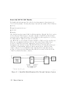
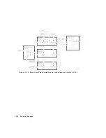
Figure
12-3
is
a
block
diagram
of
the
digital
control
functional
group
.
Theory
of
Operation
12-9
Summary of Contents for 8752C
Page 22: ...Before Applying Power 15 6 Servicing 15 6 Index Contents 16 ...
Page 38: ......
Page 43: ...Figure 2 1 Measurement Uncertainty Window System Veri cation and Performance Tests 2 5 ...
Page 116: ......
Page 122: ...Figure 3 1 Location of Major Assemblies 3 6 Adjustments and Correction Constants ...
Page 176: ......
Page 192: ...4 16 Start Troubleshooting Here ...
Page 193: ......
Page 195: ...Figure 4 7 HP 8752C Overall Block Diagram 3 of 4 Option 006 4 20 Start Troubleshooting Here ...
Page 197: ......
Page 221: ...5 24 Power Supply Troubleshooting ...
Page 222: ......
Page 271: ...Figure 7 21 A14 Generated Digital Control Signals Source Troubleshooting 7 31 ...
Page 302: ......
Page 366: ......
Page 378: ...Figure 11 4 Typical ED Re ection Test Port 11 12 Error Terms ...
Page 380: ...Figure 11 5 Typical ES Re ection Test Port 11 14 Error Terms ...
Page 382: ...Figure 11 6 Typical ER Re ection Test Port 11 16 Error Terms ...
Page 386: ...Figure 11 9 Typical ET 11 20 Error Terms ...
Page 407: ...Figure 12 5 High Band Operation of the Source Theory of Operation 12 21 ...
Page 410: ...Figure 12 6 Receiver Functional Group standard and Option 003 12 24 Theory of Operation ...
Page 411: ...Figure 12 7 Receiver Functional Group Option 003 and 004 Theory of Operation 12 25 ...
Page 412: ...Figure 12 8 Receiver Functional Group Option 006 12 26 Theory of Operation ...
Page 413: ...Figure 12 9 Receiver Functional Group Option 004 and 006 Theory of Operation 12 27 ...
Page 416: ......
Page 419: ...Figure 13 1 Module Exchange Procedure Replaceable Parts 13 3 ...
Page 423: ...Major Assemblies Replaceable Parts 13 7 ...
Page 425: ...Front Panel Assemblies Replaceable Parts 13 9 ...
Page 427: ...Rear Panel Assemblies Replaceable Parts 13 11 ...
Page 429: ...Cables Top View Replaceable Parts 13 13 ...
Page 431: ...Front Panel Cables and Attaching Hardware Replaceable Parts 13 15 ...
Page 433: ...Rear Panel Cables and Attaching Hardware Replaceable Parts 13 17 ...
Page 435: ...Source and Sampler Parts Standard and Option 003 Replaceable Parts 13 19 ...
Page 437: ...Source and Sampler Parts Option 004 006 Replaceable Parts 13 21 ...
Page 439: ...Source and Sampler Parts Options 004 and 003 004 Replaceable Parts 13 23 ...
Page 441: ...Source and Sampler Parts Option 006 Replaceable Parts 13 25 ...
Page 443: ...Display Bezel Assembly Replaceable Parts 13 27 ...
Page 445: ...Chassis Parts Replaceable Parts 13 29 ...
Page 447: ...Top View of Attaching Hardware and Post Regulator Fuses Replaceable Parts 13 31 ...
Page 449: ...Bottom View of Attaching Hardware Replaceable Parts 13 33 ...
Page 488: ......

