4.
Check
the
A1
V
olatile
Memory
a.
Turn
the
analyzer
power
on.
b.
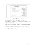
Press
4
System
5 ,
NNNNNNNNNNNNNNNNNNNNNNNNNNNNNNNNNNNNNN
SERVICE
MENU
,
NNNNNNNNNNNNNNNNN
TESTS
,
4
2
5 ,
4
x1
5 ,
NNNNNNNNNNNNNNNNNNNNNNNNNNNNNNNNNNNNNN
EXECUTE
TEST
to
run
the
internal
test
2:
A1
V
OLA
TILE
MEMORY
.
c.
Check
no
error
message
displayed.
At
the
end
of
this
test,
the
analyzer
returns
the
control
settings
to
the
default
values
(power
on
reset).
If
the
test
fails
,
the
analyzer
displays
an
error
messages
for
a
few
second
before
returning
to
the
defaults
.
If
no
error
message
is
displayed,
the
A1
volatile
memories
are
veried.
Continue
with
the
next
Check
the
A30
Front
K
eyboard.
If
one
of
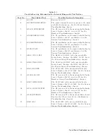
error
messages
listed
below
is
displayed,
the
A1
CPU
is
faulty
.
Replace
the
A1
CPU
.
CPU
INTERNAL
SRAM
R/W
ERROR
DSP
SRAM
R/W
ERROR
DUAL
PORT
SRAM
R/W
ERROR
CPU
BACKUP
SRAM
R/W
ERROR
5.
Check
the
A30
Front
K
eyboard
The
A30
front
keyboard
can
be
checked
using
the
external
test
17:
FRONT
P
ANEL
DIA
G.
a.
Press
4
PRESET
5 ,
4
SYSTEM
5 ,
NNNNNNNNNNNNNNNNNNNNNNNNNNNNNNNNNNNNNN
SERVICE
MENU
,
NNNNNNNNNNNNNNNNN
TESTS
,
4
1
5 ,
4
7
5 ,
4
x1
5 ,
NNNNNNNNNNNNNNNNNNNNNNNNNNNNNNNNNNNNNN
EXECUTE
TEST
to
run
the
external
test
17.
b.
Press
all
of
the
front
panel
keys
.
The
pressed
abbreviated
key
name
should
be
displayed
at
a
key
pressed.
When
you
rotate
the
RPG
knob
,
the
RPG
tuned
direction
(CW
or
CCW)
and
its
response
speed
(SLOW
,
MID
,
F
AST)
should
be
displayed.
So
you
can
check
every
key
on
the
A30
Keyboard
except
for
4
PRESET
5 .
(If
you
want
to
exit
this
test,
press
4
PRESET
5 .)
If
one
or
more
keys
seems
to
be
defective
,
replace
the
A30
front
keyboard.
If
all
keys
seem
to
be
good,
the
A30
front
keyboard
is
veried.
Continue
with
the
next
Check
the
A53
FDD.
6.
Check
the
A53
FDD
The
A53
FDD
(Flexible
Disk
Drive)
can
be
checked
using
the
external
test
18:
DISK
DR
F
ALUT
ISOL'N.
a.
Press
4
PRESET
5 ,
4
SYSTEM
5 ,
NNNNNNNNNNNNNNNNNNNNNNNNNNNNNNNNNNNNNN
SERVICE
MENU
,
NNNNNNNNNNNNNNNNN
TESTS
,
4
1
5 ,
4
8
5 ,
4
x1
5 ,
NNNNNNNNNNNNNNNNNNNNNNNNNNNNNNNNNNNNNN
EXECUTE
TEST
to
run
the
external
test
18.
b.
As
the
analyzer
instructs
,
insert
a
exible
disk
into
FDD
.
Use
a
formatted
but
blank
exible
disk,
otherwise
the
data
on
the
disk
will
be
overwritten
by
this
test.
Then
press
NNNNNNNNNNNNNN
CONT
.
c.
Check
the
test
result,
P
ASS
or
F
AIL,
that
is
displayed
at
the
end
of
the
test.
If
this
test
fails
,
replace
the
A53
FDD
.
Digital
Control
T
roubleshooting
6-11
Summary of Contents for Agilent 4396B
Page 10: ......
Page 32: ......
Page 43: ...Figure 2 7 CAL OUT Level Adjustment Location Adjustments and Correction Constants 2 11 ...
Page 46: ...Figure 2 10 Comb Generator Output 2 14 Adjustments and Correction Constants ...
Page 62: ...Figure 2 26 Final Gain Adjustment Location 2 30 Adjustments and Correction Constants ...
Page 76: ...Figure 3 1 Troubleshooting Organization 3 2 T roubleshooting ...
Page 84: ......
Page 90: ...Figure 5 1 Power Supply Lines Simpli ed Block Diagram 5 2 Power Supply T roubleshooting ...
Page 107: ...Figure 5 12 Power Supply Block Diagram 1 Power Supply T roubleshooting 5 19 ...
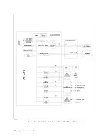
Page 108: ...Figure 5 13 Power Supply Block Diagram 2 5 20 Power Supply T roubleshooting ...
Page 109: ...Figure 5 14 Power Supply Block Diagram 3 Power Supply T roubleshooting 5 21 ...
Page 110: ......
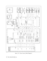
Page 112: ...Figure 6 1 Digital Control Group Simpli ed Block Diagram 6 2 Digital Control T roubleshooting ...
Page 124: ......
Page 126: ...Figure 7 1 Source Group Block Diagram 7 2 Source Group T roubleshooting ...
Page 160: ...Figure 8 1 Receiver Group Simpli ed Block Diagram 8 2 Receiver Group T roubleshooting ...
Page 168: ......
Page 184: ...Figure 10 6 External Test Setup 1 Figure 10 7 External Test Setup 2 10 10 Service Key Menus ...
Page 185: ...Figure 10 8 External Test Setup 3 Figure 10 9 External Test Setup 4 Service Key Menus 10 11 ...
Page 226: ...Figure 11 3 Power Supply Functional Group Simpli ed Block Diagram 11 6 Theory of Operation ...
Page 231: ...Figure 11 5 Digital Control Group Simpli ed Block Diagram Theory of Operation 11 11 ...
Page 235: ...Figure 11 6 Source Simpli ed Block Diagram Theory of Operation 11 15 ...
Page 244: ...Figure 11 7 Receiver Simpli ed Block Diagram 11 24 Theory of Operation ...
Page 249: ...Figure IDC5S11001 here Figure 11 8 4396B Source Group Block Diagram Theory of Operation 11 29 ...
Page 254: ...Figure 12 1 Top View Major Assemblies 12 4 Replaceable Parts ...
Page 290: ...Figure 12 36 Main Frame Assembly Parts 17 19 12 40 Replaceable Parts ...
Page 294: ......
Page 308: ......
Page 311: ...Figure C 1 Power Cable Supplied Power Requirement C 3 ...
Page 312: ......
Page 324: ......


