background image

ST

ART

HERE

The

following

procedure

veries

the

operation

of

each

assembly

in

the

source

group

by

using

the

4396B's

self-test

functions

(internal

and

external

tests).

F

or

detailed

information

about

the

self-test

functions

,

see

the

Service

K

ey

Menus.

In

this

procedure

,

the

A3A1's

divider

and

the

A6's

A/D

converter

(receiver

group)

are

veried

rst.

This

is

done

because

the

internal

tests

use

the

A/D

converter

to

measure

voltages

at

DC

bus

nodes

within

the

source

group

.

Also

,

the

A3A1's

divider

output

is

used

to

generate

the

A/D

converter's

control

signals

.

P

erform

the

following

steps

to

troubleshoot

the

source

group:

1.

Press

4

Preset

5 ,

4

System

5 ,

NNNNNNNNNNNNNNNNNNNNNNNNNNNNNNNNNNNNNNNNN

SERVICE

MENUS

,

NNNNNNNNNNNNNNNNN

TESTS

,

4

1

5 ,

4

1

5 ,

4

x1

5 ,

NNNNNNNNNNNNNNNNNNNNNNNNNNNNNNNNNNNNNN

EXECUTE

TEST

to

run

internal

test

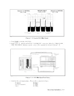
11:

A3A1

DIVIDER.

If

the

test

fails

,

there

is

a

possibility

that

the

A5

synthesizer

is

faulty

.

This

possibility

exists

because

the

A3A1

divider

obtains

the

40

MHz

reference

signal

from

A5.

P

erform

the

1.

Check

the

CAL

OUT

Signal

procedure

in

the

Check

A5

Synthesizer

Outputs

section.

This

procedure

veries

the

40

MHz

reference

signal.

If

the

CAL

OUT

signal

is

good,

A3A1

is

probably

faulty

.

Replace

A3A1.

If

the

CAL

OUT

signal

is

bad,

replace

A5.

2.

Press

4

5

5 ,

4

x1

5 ,

NNNNNNNNNNNNNNNNNNNNNNNNNNNNNNNNNNNNNN

EXECUTE

TEST

to

run

internal

test

5:

A6

A/D

CONVERTER.

If

the

test

fails

,

replace

A6

in

the

receiver

group

.

3.

Press

4

6

5 ,

4

x1

5 ,

NNNNNNNNNNNNNNNNNNNNNNNNNNNNNNNNNNNNNN

EXECUTE

TEST

to

run

internal

test

6:

A5

REFERENCE

OSC.

If

the

test

fails

,

replace

A5.

4.

Press

4

7

5 ,

4

x1

5 ,

NNNNNNNNNNNNNNNNNNNNNNNNNNNNNNNNNNNNNN

EXECUTE

TEST

to

run

internal

test

7:

A5

FRA

CTIONAL

N

OSC.

If

the

test

fails

,

replace

A5.

5.

Press

4

8

5 ,

4

x1

5 ,

N

NNNNNNNNNNNNNNNNNNNNNNNNNNNNNNNNNNNNN

EXECUTE

TEST

to

run

internal

test

8:

A5

STEP

OSC.

If

the

test

fails

,

replace

A5.

6.

Press

4

9

5 ,

4

x1

5 ,

NNNNNNNNNNNNNNNNNNNNNNNNNNNNNNNNNNNNNN

EXECUTE

TEST

to

run

internal

test

9:

A4A1

1st

LO

OSC.

If

the

test

fails

,

replace

A4.

7.

Press

4

1

5 ,

4

3

5 ,

4

x1

5 ,

NNNNNNNNNNNNNNNNNNNNNNNNNNNNNNNNNNNNNN

EXECUTE

TEST

to

run

internal

test

13:

A3A1

SOURCE

OSC.

If

the

test

fails

,

replace

A3A1.

8.

Press

4

1

5 ,

4

6

5 ,

4

x1

5 ,

NNNNNNNNNNNNNNNNNNNNNNNNNNNNNNNNNNNNNN

EXECUTE

TEST

to

run

internal

test

16:

A3A1

ALC.

If

the

test

fails

,

A3A1,

A3A2,

or

A3A3

is

probably

faulty

.

V

erify

A3A1,

A3A2,

and

A3A3

in

accordance

with

the

Check

an

A3A1

ALC

Output,

Check

A3A2

2nd

LO

Outputs,

and

Check

an

A3A3

Source

Output

sections

in

this

chapter

.

9.

Press

4

1

5 ,

4

0

5 ,

4

x1

5 ,

N

NNNNNNNNNNNNNNNNNNNNNNNNNNNNNNNNNNNNN

EXECUTE

TEST

to

run

internal

test

10:

A3A2

2ND

LO

OSC.

If

the

test

fails

,

replace

A3A2.

10.

Press

4

2

5 ,

4

0

5 ,

4

x1

5 ,

NNNNNNNNNNNNNNNNNNNNNNNNNNNNNNNNNNNNNN

EXECUTE

TEST

to

run

internal

test

20:

OUTPUT

A

TTENU

A

TOR.

Then

connect

the

equipment

as

shown

in

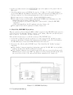
Figure

7-2

and

press

NNNNNNNNNNNNNNNNNNNNNNNNNN

CONTINUE

to

start

the

test.

If

the

test

fails

,

the

A7

Output

Attenuator

is

probably

faulty

.

P

erform

the

procedure

provided

in

the

A7

Output

Attenuator

Control

Signals

section

to

conrm

that

A7

is

faulty

.

Source

Group

T

roubleshooting

7-5

Summary of Contents for Agilent 4396B

Page 1: ...uments with serial number pre x JP1KD or rmware revision 1 00 For additional important information about serial numbers read Serial Number in Appendix A Agilent Part No 04396 90121 Printed in Japan March 2001 Third Edition Silicon Investigations Repair Information Contact Us 920 955 3693 www siliconinvestigations com ...

Page 2: ...y copyright All rights are reserved No part of this document may be photocopied reproduced or translated to another language without the prior written consent of the Agilent Technologies Agilent Technologies Japan Ltd Component Test PGU Kobe 1 3 2 Murotani Nishi ku Kobe shi Hyogo 651 2241 Japan c Copyright Agilent Technologies Japan Ltd 1997 2000 2001 ...

Page 3: ...ion is printed Minor corrections and updates that are incorporated at reprint do not cause the date to change The manual part number changes when extensive technical changes are incorporated May 1997 First Edition part number 04396 90121 June 2000 Second Edition part number 04396 90121 March 2001 Third Edition part number 04396 90121 iii ...

Page 4: ...losive Atmosphere Do not operate the instrument in the presence of ammable gasses or fumes Operation of any electrical instrument in such an environment constitutes a de nite safety hazard Keep Away From Live Circuits Operating personnel must not remove instrument covers Component replacement and internal adjustments must be made by quali ed maintenance personnel Do not replace components with the...

Page 5: ... Out position of push button switch Frame or chassis terminal A connection to the frame chassis of the equipment which normally include all exposed metal structures This Warning sign denotes a hazard It calls attention to a procedure practice condition or the like which if not correctly performed or adhered to could result in injury or death to personnel This Caution sign denotes a hazard It calls...

Page 6: ...ice facility designated by Agilent Technologies Buyer shall prepay shipping charges to Agilent Technologies and Agilent Technologies shall pay shipping charges to return the product to Buyer However Buyer shall pay all shipping charges duties and taxes for products returned to Agilent Technologies from another country Agilent Technologies warrants that its software and rmware designated by Agilent...

Page 7: ... incidental or consequential damages whether based on contract tort or any other legal theory Assistance Product maintenance agreements and other customer assistance agreements are available for Agilent Technologies products For any assistance contact your nearest Agilent Technologies Sales and Service O ce Addresses are provided at the back of this manual vii ...

Page 8: ...es when a name or a variable must be typed in place of the words in italics For example copy lename means to type the word copy to type a space and then to type the name of a le such as file1 Computer Computer font is used for on screen prompts and messages 4HARDKEYS5 Labeled keys on the instrument front panel are enclosed in 4 5 NNNNNNNNNNNNNNNNNNNNNNNNNN SOFTKEYS Softkeys located to the right of...

Page 9: ...use BASIC program to control the analyzer and describes how HP Instrument BASIC works with the analyzer GPIB Command Reference The GPIB Command Reference provides a summary of all available GPIB commands It also provides information on the status reporting structure and the trigger system these features conform to the SCPI standard HP Instrument BASIC Manual Set The HP Instrument BASIC User s Hand...

Page 10: ......

Page 11: ...llator Frequency Adjustment 2 6 Required Equipment 2 6 Procedure 2 6 520 MHz Level Adjustment 2 8 Required Equipment 2 8 Procedure 2 8 CAL OUT Level Adjustment 2 10 Required Equipment 2 10 Procedure 2 10 Comb Generator Adjustment 2 12 Required Equipment 2 12 Procedure 2 12 Step Pretune Correction Constants 2 15 Required Equipment 2 15 Procedure 2 15 Second Local PLL Lock Adjustment 2 16 Required E...

Page 12: ...2 39 Required Equipment 2 39 Procedure 2 39 10 MHz Reference Oscillator Frequency Adjustment Option 1D5 Only 2 41 Required Equipment 2 41 Procedure 2 41 3 Troubleshooting INTRODUCTION 3 1 TROUBLESHOOTING SUMMARY 3 1 START HERE 3 3 INSPECT THE POWER ON SEQUENCE 3 4 Check the Fan 3 4 Check the Front Panel LEDs and Displays 3 4 Check Error Message 3 4 OPERATOR S CHECK 3 5 Test Equipment 3 5 Procedure...

Page 13: ...1 CPU 5 11 4 Remove Assemblies 5 12 TROUBLESHOOT THE FAN AND THE A50 DC DC CONVERTER 5 13 1 Troubleshoot the Fan 5 13 2 Troubleshoot the A50 DC DC Converter 5 14 TROUBLESHOOT THE A2 POST REGULATOR 5 16 1 Check the A40 Pre Regulator 5 16 2 Check the A50 DC DC Converter 5 16 3 Remove Assemblies 5 16 4 Measure the A2 Post Regulator Output Voltages 5 16 6 Digital Control Troubleshooting INTRODUCTION 6...

Page 14: ...3 7 19 2 Check the 1st LO OSC Signal at A4A1J4 7 21 CHECK AN A3A1 ALC OUTPUT 7 23 1 Check the 21 42 MHz Signal 7 23 CHECK A3A2 2ND LO OUTPUTS 7 26 1 Check the 2nd Local Oscillator Signal 7 26 2 Check the 2 05858 GHz Signal 7 27 CHECK AN A3A3 SOURCE OUTPUT 7 30 1 Check the A3A3 RF Signal 7 30 CHECK A7 OUTPUT ATTENUATOR CONTROL SIGNALS 7 32 1 Check A7 Control Signals 7 32 CHECK THE A60 HIGH STABILIT...

Page 15: ...NNNNNNNNNNNNNNNNNNNNNNNNNNNNNNNNNNNNN EXTERNAL TESTS DIAG TEST 17 10 5 NNNNNNNNNNNNNNNNNNNNNNNNNNNNNNNNNNNNNNNNNNNNNNNNNN ADJUSTMENT TESTS DIAG TEST 41 10 5 NNNNNNNNNNNNNNNNNNNNNNNNNNNNNNNNNNNNNNNNN DISPLAY TESTS DIAG TEST 48 10 5 NNNNNNNNNNNNNNNNNNNNNNNNNNNNNNNNNNNNNNNNN ALL EXT TESTS DIAG TEST 53 10 5 NNNNNNNNNNNNNNNNNNNNNNNNNNNNNNNN MISC TESTS DIAG TEST 58 10 5 Test Status 10 5 Diagnostic Tests...

Page 16: ...DJ 10 16 46 3 MHZ BPF ADJ 10 16 47 1 MHZ BPF ADJ 10 16 NNNNNNNNNNNNNNNNNNNNNNNNNNNNNNNNNNNNNNNNN DISPLAY TESTS 10 16 48 TEST PATTERN 1 10 16 49 TEST PATTERN 2 10 17 50 TEST PATTERN 3 10 17 51 TEST PATTERN 4 10 17 52 TEST PATTERN 5 10 17 NNNNNNNNNNNNNNNNNNNNNNNNNNNNNNNNNNNNNNNNN ALL EXT TESTS 10 17 53 ALL EXT 1 10 17 54 ALL EXT 2 10 17 55 ALL EXT 3 10 17 56 ALL EXT 4 10 17 57 ALL EXT 5 10 17 NNNNNN...

Page 17: ... 27 21 FN INTEG OUT Fractional N Oscillator Integrator Output Voltage 10 28 22 REF VTUNE Reference Oscillator VCO Tuning Voltage 10 29 23 3RD LO VTUNE Third Local Oscillator VCO Tuning Voltage 10 29 24 2ND IF LVL Second IF Signal Level 10 29 25 AD VREF A D Converter Voltage Reference 10 29 26 GND Ground 10 30 Frequency Bus Node Descriptions 10 30 0 OFF 10 30 1 SOURCE OSC Source Oscillator 10 30 2 ...

Page 18: ...B50 DB60 10 43 NNNNNNNNNNNNNNNNNNNNNNNNNNNNNNNNNNNNNNNNNNNNNNNNNN LVL DAC AUTO man DIAG SERV SOUR LEV DAC MODE AUTO MAN 10 44 NNNNNNNNNNNNNNNNNNNNNNNNNNNNNNNNNNNNNNNNN LVL DAC VALUE DIAG SERV SOUR LEV DAC VAL numeric 10 44 NNNNNNNNNNNNNNNNNNNNNNNNNNNNNNNNNNNNNNNNNNNNNNNNNNNNN GAIN DAC AUTO man DIAG SERV SOUR GAIN DAC MODE AUTO MAN 10 44 NNNNNNNNNNNNNNNNNNNNNNNNNNNNNNNNNNNNNNNNNNNN GAIN DAC VALUE D...

Page 19: ...11 19 Source OSC 11 19 ALC 11 20 A3A2 2nd LO 11 20 2nd Local OSC Circuit 11 20 Source First Mixer 11 21 A3A3 Source 11 21 A7 Output Attenuator 11 21 RECEIVER THEORY 11 23 A8 Input Attenuator 11 25 A9 Input Multiplexer 11 25 A4A2 Receiver RF 11 25 A6 Receiver IF 11 26 IF BPFs and LPFs 11 26 3rd Converter and 3rd LO 11 27 Sample Hold A D Converter and Sequencer 11 27 Gains W X Y and Z and Ranges F a...

Page 20: ... Number A 2 B A20 Motherboard Pin Assignment C Power Requirement Replacing Fuse C 1 Fuse Selection C 1 Power Requirements C 2 Power Cable C 2 Messages Error Messages in Alphabetical Order Messages 1 Error Messages in Numerical Order Messages 9 Index Contents 10 ...

Page 21: ...26 2 24 Band Pass Filters Adjustment Locations 2 27 2 25 Final Gain Adjustment Setup 2 29 2 26 Final Gain Adjustment Location 2 30 2 27 Second Local Leakage Adjustment Location 2 31 2 28 Second Local Leakage Adjustment Setup 2 32 2 29 RF OUT Level Correction Constants Setup 2 33 2 30 Spectrum Analyzer Absolute Magnitude Correction Constants Setup 2 34 2 31 Network Analyzer Absolute Magnitude Corre...

Page 22: ...Signal 7 11 7 8 Typical FRAC N OSC Signal in Frequency Bus Measurement 7 12 7 9 FRAC N OSC Signal Level Test Setup 7 12 7 10 FRAC N OSC Typical Signal 7 13 7 11 STEP OSC Test Setup 7 14 7 12 Typical STEP OSC Signal at Center 0 Hz 7 16 7 13 Typical 520 MHz Signal 7 17 7 14 520 MHz Signal Test Setup 7 17 7 15 EXT REF Test Setup 7 18 7 16 1st LO OSC Signal Test Setup 7 19 7 17 Typical 1st LO OSC Sign...

Page 23: ...Diagram 11 29 11 9 4396B Receiver Group Block Diagram 11 30 12 1 Top View Major Assemblies 12 4 12 2 Bottom View Major Assemblies 12 6 12 3 Angle Assembly Parts 1 3 12 7 12 4 Angle Assembly Parts 2 3 12 8 12 5 Angle Assembly Parts 3 3 12 9 12 6 ATT Assembly Parts 1 2 12 10 12 7 ATT Assembly Parts 2 2 12 11 12 8 Front Assembly Parts 1 5 12 12 12 9 Front Assembly Parts 2 5 12 13 12 10 Front Assembly...

Page 24: ...19 Front Bezel Assembly 12 37 12 34 Main Frame Assembly Parts 15 19 A2 Post Regulator Assembly 12 38 12 35 Main Frame Assembly Parts 16 19 A5 and A6 Assemblies 12 39 12 36 Main Frame Assembly Parts 17 19 12 40 12 37 Main Frame Assembly Parts 18 19 RF Cable Assemblies 12 41 12 38 Main Frame Assembly Parts 19 19 Option 1D5 12 42 12 39 A9 N Type Connector Replacement 12 43 A 1 Serial Number Plate A 2...

Page 25: ...Settings 11 28 12 1 Manufacturers Code List 12 2 12 2 List of Abbreviations 12 3 12 3 Top View Major Assemblies 12 5 12 4 Bottom View Major Assemblies 12 6 12 5 Angle Assembly Parts 1 3 12 7 12 6 Angle Assembly Parts 2 3 12 8 12 7 Angle Assembly Parts 3 3 12 9 12 8 ATT Assembly Parts 1 2 12 10 12 9 ATT Assembly Parts 2 2 12 11 12 10 Front Assembly Parts 1 5 12 12 12 11 Front Assembly Parts 2 5 12 ...

Page 26: ... 19 A50 DC DC Converter Assembly 12 35 12 34 Main Frame Assembly Parts 13 19 A51 GSP Assembly 12 36 12 35 Main Frame Assembly Parts 14 19 Front Bezel Assembly 12 37 12 36 Main Frame Assembly Parts 15 19 A2 Post Regulator Assembly 12 38 12 37 Main Frame Assembly Parts 16 19 A5 and A6 Assemblies 12 39 12 38 Main Frame Assembly Parts 18 19 RF Cable Assemblies 12 41 12 39 Main Frame Assembly Parts 19 ...

Page 27: ... PN 04396 18030 Note The next seven gray tabbed chapters are the core troubleshooting chapters Troubleshooting The troubleshooting strategy is to systematically verify portions of the analyzer and thus narrow down the cause of a problem to the defective assembly This chapter is the rst of a series of troubleshooting procedures It checks the operation of the analyzer independent of system periphera...

Page 28: ...ch functional group Replaceable Parts provides part numbers and illustrations of the replaceable assemblies and miscellaneous chassis parts together with ordering information Post Repair Procedures contains the table of related service procedures It is a table of adjustments and veri cation procedures to be performed after repair or replacement of each assembly Appendices contains the manual chang...

Page 29: ...icro oppy Disk Drive 1 A Program 4396B Adjustments Program 3 5 inch PN 04396 18030 1 A Frequency Counter Frequency Range 20 MHz to 1 GHz Time Base Error 61 921007 year 5343A Opt 0013 1 P A Frequency Standard4 Frequency 10 MHz Time Base Error 61210010 year 5061B 1 P Spectrum Analyzer Frequency Range 100 kHz to 4 GHz 8566A B 1 P A T Network Analyzer Frequency Range 300 kHz to 1 8 GHz 8753A B C 1 P P...

Page 30: ...ation 909C Opt 012 or part of 85032B5 3 P A T 6 dB Fixed Attenuation 50 N m N f 8491A Opt 006 2 P 6 dB Fixed Attenuation 50 N m N f VSWR 1 015 8491A Opt 006 Opt H606 2 P Two Way Power Splitter Frequency Range 100 kHz to 1 8 GHz Output Tracking 0 15 dB 11667A 1 P A T Cables Type N cable 50 11500B or part of 11851B7 4 P A T RF cable kit 11851B 1 P A BNC cable 61 cm 50 PN 8120 1839 1 P A T BNC cable ...

Page 31: ...0 PN 1250 0832 1 A SMB f BNC f adapter 50 PN 1250 1236 1 A N f BNC f adapter 50 PN 1250 1474 1 P N m N m adapter 50 PN 1250 1475 1 P A T N m BNC f adapter 50 PN 1250 1476 1 P A T N f BNC m adapter 50 PN 1250 1477 1 P A T SMA m BNC f adapter 50 PN 1250 1548 1 T SMA m SMA f right angle adapter 50 PN 1250 1741 1 A T APC3 5 m APC3 5 f adapter 50 PN 1250 1866 1 P A APC7 5 N f adapter 50 11524A or part ...

Page 32: ......

Page 33: ...he operator and to keep the instrument in a safe and serviceable condition The adjustments must be performed by quali ed service personnel Warning Any interruption of the protective ground conductor inside or outside the analyzer or disconnection of the protective ground terminal can make the instrument dangerous Intentional interruption of the protective ground system for any reason is prohibited...

Page 34: ...s Order Of Adjustments When performing more than one Adjustments or Correction Constants procedure perform them in the order they appear in this chapter The procedures are presented in the following order 40 MHz Reference Oscillator Frequency Adjustment 520 MHz Level Adjustment CAL OUT Level Adjustment Comb Generator Adjustment Step Pretune Correction Constants Second Local PLL Lock Adjustment DC ...

Page 35: ...essing 4RETURN5 or 4SELECT5 4ENTER5 or 4EXECUTE5 if Nimitz Keyboard 3 If NNNNNNNNNNNNNN QUIT or NNNNNNNNNNNNNN EXIT is displayed in a menu select one of these to exit the menu Otherwise press 4 5 4CONTINUE5 if Nimitz Keyboard to exit When you exit menus the program displays another menu Note Press 4 5 to access on screen help information for the selection you have highlighted Help information appe...

Page 36: ... in Table 2 1 Table 2 1 Required Binaries Name Version Description GRAPH 5 2 Graphics GRAPHX 5 2 Graphics Extensions IO 5 1 I O MAT 5 1 Matrix Statements PDEV 5 0 Program Development KBD 5 1 Keyboard Extensions CLOCK 5 0 Clock MS 5 1 Mass Storage ERR 5 1 Error Message DISC 5 0 Small Disc Driver CS80 5 0 CS80 Disc Driver GPIB 5 0 GPIB Interface Driver FGPIB 5 0 GPIB Interface Driver CRTB 5 2 Bit ma...

Page 37: ...re the Adjustment Program ADJ4396B will be run 3 Set the mass storage unit speci er MSUS to the address of the drive or the directory where TE A4396B is located 4 Load and run TE A4396B 5 Follow the instructions on the controller s screen until the program ends 6 Set the mass storage unit speci er MSUS to the address of the drive or the directory where the Adjustment Program ADJ4396B is located 7 ...

Page 38: ...cm PN 8120 1839 Procedure 1 Connect the equipment as shown in Figure 2 2 Figure 2 2 40 MHz Reference Oscillator Frequency Adjustment Setup 2 Set the frequency counter as follows Input Impedance 50 Frequency Range 10 Hz 500 MHz 3 Adjust A5 40 MHz FREQ ADJ until the frequency counter reading is within 20 MHz 6 2 Hz The adjustment location is shown in Figure 2 4 2 6 Adjustments and Correction Constan...

Page 39: ...Figure 2 3 40 MHz Reference Oscillator Frequency Adjustment Location Adjustments and Correction Constants 2 7 ...

Page 40: ...f adapter PN 1250 0832 N m BNC f adapter PN 1250 1476 BNC cable 61 cm PN 8120 1839 Procedure 1 Turn the analyzer OFF 2 Remove the J cable from the A5 520 MHz OUT connector The connector location is shown in Figure 2 4 Figure 2 4 520 MHz Level Adjustment Location 3 Connect the equipment as shown in Figure 2 5 2 8 Adjustments and Correction Constants ...

Page 41: ...00 kHz 5 Turn the 4396B analyzer ON 6 Adjust A5 520 MHz LEVEL ADJ until the spectrum analyzer reading for 520 MHz signal level is within 015 6 0 2 dBm The adjustment location is shown in Figure 2 4 7 Turn the 4396B analyzer OFF 8 Reconnect the J cable to the A5 520 MHz OUT connector Adjustments and Correction Constants 2 9 ...

Page 42: ...477 Procedure 1 Connect the power sensor to the power meter Calibrate the power meter for the power sensor 2 Connect the equipment as shown in Figure 2 6 Figure 2 6 CAL OUT Level Adjustment Setup 3 Adjust A5 CALIBRATOR LEVEL ADJ until the power meter reading is within 020 60 2 dBm The adjustment location is shown in Figure 2 7 2 10 Adjustments and Correction Constants ...

Page 43: ...Figure 2 7 CAL OUT Level Adjustment Location Adjustments and Correction Constants 2 11 ...

Page 44: ...lyzer 8566A B SMB f BNC f adapter PN 1250 1236 N m BNC f adapter PN 1250 1476 BNC cable 122 cm PN 8120 1840 Procedure 1 Turn the 4396B analyzer OFF 2 Connect the equipment as shown in Figure 2 8 A5 COMB OUT connector location is shown in Figure 2 9 Figure 2 8 Comb Generator Adjustment Setup 2 12 Adjustments and Correction Constants ...

Page 45: ...the 4396B analyzer ON 5 Adjust A5 COMB DC BIAS ADJ until the spectrum analyzer display meets the following requirements 720 MHz Signal Level between 046 and 037 dBm 480 MHz to 920 MHz Flatness 8 dB 480 MHz to 920 MHz Signal Level 051 dBm The adjustment location is shown in Figure 2 9 The typical spectrum analyzer display is shown in Figure 2 10 Adjustments and Correction Constants 2 13 ...

Page 46: ...Figure 2 10 Comb Generator Output 2 14 Adjustments and Correction Constants ...

Page 47: ... loop oscillator Required Equipment None Procedure 1 Run the adjustment program and display the main menu see Updating Correction Constants using the Adjustments Program 2 Choose the Step Pretune Correction Constants 3 Follow the adjustment program instructions to update the correction constants Adjustments and Correction Constants 2 15 ...

Page 48: ...NC f adapter PN 1250 1476 BNC cable 122 cm PN 8120 1840 Procedure 1 Turn the 4396B analyzer OFF 2 Remove the D cable from the A3A1 ALC Out connector Remove the I cable from the A3A2 Second Local Out connector The connector locations are shown in Figure 2 11 Figure 2 11 Second Local PLL Adjustment Location 3 Connect the equipment as shown in Figure 2 12 2 16 Adjustments and Correction Constants ...

Page 49: ...NNNNNNNNNNNNNNNNNNNNNNNNNN EXECUTE TEST 7 Adjust A3A2 Second Local Adj until 2 08 GHz appears constantly on the spectrum analyzer display and the 4396B analyzer reading is between the limit lines If 2 24 GHz appears rotate Second Local Adj clockwise If 1 92 GHz appears rotate Second Local Adj counterclockwise The adjustment location is shown in Figure 2 11 8 Turn the analyzer OFF 9 Reconnect the I...

Page 50: ...ut Place the board on the analyzer with the component side facing upward 4 Remove the shield case from the board 5 Pull the plugs that block the DC OFFSET ADJ holes out see Figure 2 13 If you are also going to do the 0 90 tracking adjustment pull the other two plugs out Figure 2 13 Plug Locations 6 Replace the shield case on the A6 board Replace the A6 board into the slot 7 Connect the equipment a...

Page 51: ... 2 15 DC O set and Hold Step Adjustment Locations 8 Set the oscilloscope as follows INPUT Range 400 mV Coupling DC 1 M TIMBASE Range 50 S 9 Turn the analyzer ON 10 Press the following keys to execute adjust test No 41 Adjustments and Correction Constants 2 19 ...

Page 52: ...own in Figure 2 16 The adjustment location is shown in Figure 2 15 Note If the waveform doesn t appear on the oscilloscope display change the oscilloscope range setting to 4 V to adjust coarsely Figure 2 16 DC O set Adjustment Waveform 12 Adjust 0 deg HOLD STEP ADJ until the voltage di erence between the longer step and shorter step is smaller than 50 mV as shown in Figure 2 17 The adjustment loca...

Page 53: ... NNNNNNNNNNNNNN CONT to nish the adjustment Note Steps 16 to 19 replace the plugs into the DC OFFSET ADJ holes If you are going to do the 0 90 tracking adjustment skip these steps 16 Turn the analyzer OFF 17 Pull the A6 board out Place the board on the analyzer with the component side facing upward 18 Replace the plugs into the DC OFFSET ADJ holes see Figure 2 18 Adjustments and Correction Constan...

Page 54: ...Figure 2 18 Plug Locations 19 Replace the A6 board into the slot 2 22 Adjustments and Correction Constants ...

Page 55: ...ol keys side Note Steps 3 to 6 pull the plugs that block the TRACKING ADJ holes out If these plugs are already out skip these steps 3 Pull the A6 board out Place the board on the analyzer with the component side facing upward 4 Remove the shield case from the board 5 Pull the plugs that block the TRACKING ADJ holes see Figure 2 19 Figure 2 19 Plug Locations 6 Replace the shield case on the A6 boar...

Page 56: ...NNNNNNNNNNNNNNNNNNNNNNNNNN EXECUTE TEST 10 Adjust PHASE and GAIN of 0 90 deg TRACKING ADJ until the analyzer s marker reading of magnitude is smaller than 0 1 U The smallest circle of the analyzer display shows the adjustments limit Adjustment locations are shown in Figure 2 21 Figure 2 21 0 90 Tracking Adjustment Locations 11 Press NNNNNNNNNNNNNN CONT to nish the adjustment 2 24 Adjustments and C...

Page 57: ...alyzer with the component side facing upward 14 Replace the plugs into the TRACKING ADJ holes see Figure 2 22 If the plugs for the DC OFFSET ADJ are out replace the plugs Figure 2 22 Plug Locations 15 Replace the A6 board into the slot Adjustments and Correction Constants 2 25 ...

Page 58: ...eys side 3 Connect the equipment as shown in Figure 2 23 Figure 2 23 Band Pass Filters Adjustments Setup 4 Turn the analyzer ON 5 Press the following keys to execute adjust test No 46 4PRESET5 4SYSTEM5 NNNNNNNNNNNNNNNNNNNNNNNNNNNNNNNNNNNNNN SERVICE MENU NNNNNNNNNNNNNNNNN TESTS 445 465 4x15 NNNNNNNNNNNNNNNNNNNNNNNNNNNNNNNNNNNNNN EXECUTE TEST 6 Adjust BW s of 3 MHz BPF ADJ until the analyzer measure...

Page 59: ...NNNNNNNNNNN CONT to nish the 3 MHz band pass lter adjustment 1 MHz BPF Band Width Adjustment 12 Press the following keys to execute adjust test No 47 4PRESET5 4SYSTEM5 NNNNNNNNNNNNNNNNNNNNNNNNNNNNNNNNNNNNNN SERVICE MENU NNNNNNNNNNNNNNNNN TESTS 445 475 4x15 NNNNNNNNNNNNNNNNNNNNNNNNNNNNNNNNNNNNNN EXECUTE TEST 13 Adjust BW s of 1 MHz BPF ADJ until the analyzer measurement trace is within the limits a...

Page 60: ...djust GAIN of 1 MHz BPF ADJ until the analyzer reading of marker magnitude is between 01 6 0 1 dBm and PASS is displayed The adjustment location is shown in Figure 2 24 18 Press NNNNNNNNNNNNNN CONT to nish the 1 MHz band pass lter adjustment 2 28 Adjustments and Correction Constants ...

Page 61: ...Adjustment Setup 2 Press the following keys to execute adjust test No 43 4PRESET5 4SYSTEM5 NNNNNNNNNNNNNNNNNNNNNNNNNNNNNNNNNNNNNN SERVICE MENU NNNNNNNNNNNNNNNNN TESTS 445 435 4x15 NNNNNNNNNNNNNNNNNNNNNNNNNNNNNNNNNNNNNN EXECUTE TEST 3 Set the signal generator as follows Frequency 20 MHz Amplitude 0 dBm 4 Adjust FINAL GAIN ADJ until the analyzer reading is between the limit lines and PASS is display...

Page 62: ...Figure 2 26 Final Gain Adjustment Location 2 30 Adjustments and Correction Constants ...

Page 63: ...r PN 1250 0781 SMA m SMA f right angle adapter PN 1250 1741 BNC cable 61 cm PN 8120 1839 BNC cable 122 cm 2 required PN 8120 1840 Type N Cable 61 cm 2 required 11500B or part of 11851B Procedure 1 Turn the analyzer OFF 2 Remove the C cable from the A3A3 rst local input connector The connector location is shown in Figure 2 27 Figure 2 27 Second Local Leakage Adjustment Location 3 Connect the equipm...

Page 64: ...the signal generators as follows Signal Generator 1 Setting Signal Generator 2 Setting Frequency 100 MHz 2 18 GHz Amplitude 0 dBm 04 dBm 7 Adjust second local leakage adjustments until the analyzer s marker reading of magnitude is smaller than 5 mU and PASS is displayed The smallest circle of the analyzer display shows the adjustments limit The adjustment locations are shown in Figure 2 27 8 Recon...

Page 65: ...cedure 1 Run the adjustment program and display the main menu see Updating Correction Constants using the Adjustments Program 2 Choose the RF OUT Level Correction Constants 3 Follow the adjustment program instructions to update the correction constants Figure 2 29 shows the equipment setup for the Correction Constants Figure 2 29 RF OUT Level Correction Constants Setup Adjustments and Correction C...

Page 66: ...apter PN 1250 1475 Type N Cable 61 cm 11500B or part of 11851B Procedure 1 Run the adjustment program and display the main menu see Updating Correction Constants using the Adjustments Program 2 Choose the SA Absolute Magnitude Correction Constants 3 Follow the adjustment program instructions to update the correction constants Figure 2 30 shows the equipment setup for the Correction Constants Figur...

Page 67: ...pter PN 1250 1475 Type N Cable 61 cm 11500B or part of 11851B Procedure 1 Run the adjustment program and display the main menu see Updating Correction Constants using the Adjustments Program 2 Choose the NA Absolute Magnitude Correction Constants 3 Follow the adjustment program instructions to update the correction constants Figure 2 31 shows the equipment setup for the Correction Constants Figure...

Page 68: ...of 11851B Procedure 1 Run the adjustment program and display the main menu see Updating Correction Constants using the Adjustments Program 2 Choose the Crystal Filter Correction Constants 3 Follow the adjustment program instructions to update the correction constants Figure 2 32 shows the equipment setup for the Correction Constants Figure 2 32 Crystal Filter Correction Constants Setup 2 36 Adjust...

Page 69: ... or part of 11851B Procedure 1 Run the adjustment program and display the main menu see Updating Correction Constants using the Adjustments Program 2 Choose the IF Gain Errors Correction Constants 3 Follow the adjustment program instructions to update the correction constants Figure 2 33 and Figure 2 34 show the equipment setups for the Correction Constants Figure 2 33 IF Gain Errors Correction Co...

Page 70: ...Figure 2 34 IF Gain Errors Correction Constants Setup 2 2 38 Adjustments and Correction Constants ...

Page 71: ...gram and display the main menu see Updating Correction Constants using the Adjustments Program 2 Choose the NA Magnitude Ratio Phase Correction Constants 3 Follow the adjustment program instructions to update the correction constants Figure 2 35 and Figure 2 36 show the equipment setups for the Correction Constants Two measurements are done for each of A R and B R changing the power splitter conne...

Page 72: ...Figure 2 36 Network Analyzer Magnitude Ratio Phase Correction Constants Setup 2 2 40 Adjustments and Correction Constants ...

Page 73: ...nalyzer with the bracket facing upward The A60 location is shown in Figure 2 37 Figure 2 37 10 MHz Reference Oscillator Frequency Adjustment Location Note The analyzer must be ON continuously for at least 24 hours immediately prior to the oscillator adjustment This warm up time allows both the temperature and frequency of the oscillator to stabilize Failure to allow su cient stabilization time cou...

Page 74: ...4G n5 Frequency Span 0 Hz 4Span5 NNNNNNNNNNNNNNNNNNNNNNNNNNNNNNNNNNN ZERO SPAN Source Power 020 dBm 4Source5 NNNNNNNNNNNNNNNNN POWER 405 425 405 4x15 6 Set the frequency counter as follows Input Impedance 50 Frequency Range 500 MHz 26 5 GHz 7 Remove the dust cap screw on the A60 assembly to gain access to the adjustment screw 8 Adjust the A60 adjustment screw until the frequency counter reading is...

Page 75: ...o the appropriate chapter The ve functional groups are power supply digital control source receiver and accessories Descriptions of these groups are provided in the Theory of Operation chapter Isolate Faulty Group Troubleshooting the next chapter assumes that the fault is within one of two functional groups source receiver Isolate Faulty Group Troubleshooting identi es the faulty group and refers ...

Page 76: ...Figure 3 1 Troubleshooting Organization 3 2 T roubleshooting ...

Page 77: ...ON SEQUENCE in this chapter 3 Perform the OPERATOR s CHECK in this chapter 4 Perform the INSPECT THE REAR PANEL FEATURE in this chapter If the analyzer has passed all of the checks in steps 2 through 4 but it still making incorrect measurements or unexpected operations suspect the accessories Accessories such as RF or interconnect cables calibration and veri cation kit devices test set can all ind...

Page 78: ... turns on and the analyzer displays Internal Test In Progress for several seconds 3 The analyzer displays the graticule If case of unexpected results continue with Digital Control Troubleshooting chapter Check Error Message Turn the analyzer power on Inspect the LCD No error message should be displayed If one of the error message or a status annotation listed below appears on the LCD continue with...

Page 79: ... required 11500B or part of 11851B BNC cable 30 cm PN 8120 1838 N m N m adapter PN 1250 1475 N m BNC f adapter PN 1250 1476 Procedure 1 Turn the analyzer power on 2 Press 4PRESET5 to initialize the analyzer 3 Press 4SYSTEM5 NNNNNNNNNNNNNNNNNNNNNNNNNNNNNNNNNNNNNN SERVICE MENU NNNNNNNNNNNNNNNNN TESTS 455 435 4x15 to access the ALL EXT 1 test When TEST 53 ALL EXT 1 appears on the LCD press NNNNNNNNNN...

Page 80: ...ect the equipment as shown in Figure 3 4 Then press NNNNNNNNNNNNNN CONT Figure 3 4 ALL EXT 2 Test Setup 8 Wait until the analyzer displays PASS or FAIL If the ALL EXT 2 test fails continue with step 18 9 Press 4 5 to access the ALL EXT 3 test Then press NNNNNNNNNNNNNNNNNNNNNNNNNNNNNNNNNNNNNN EXECUTE TEST to execute the test 10 At the prompt connect the equipment as shown in Figure 3 5 Then press N...

Page 81: ...nue with step 18 12 Press 4 5 to access the ALL EXT 4 test Then press NNNNNNNNNNNNNNNNNNNNNNNNNNNNNNNNNNNNNN EXECUTE TEST 13 At the prompt connect the equipment as shown in Figure 3 6 Then press NNNNNNNNNNNNNN CONT Figure 3 6 ALL EXT 4 Test Setup 14 Wait until the analyzer displays PASS or FAIL T roubleshooting 3 7 ...

Page 82: ...T Figure 3 7 ALL EXT 5 Test Setup 17 Wait until the analyzer displays PASS or FAIL 18 If one or some of the ALL EXT tests fail Recheck the equipment con guration and connections if necessary retest Con rm that the power splitter terminations and cables meet their published speci cations Visually inspect the connectors If necessary retest If the tests still fail continue with the Isolate Faulty Gro...

Page 83: ...must be installed in the controller see the manuals of the controller and the BASIC system I O and GPIB binaries loaded see the manuals of the BASIC system Select code see the manuals of the BASIC system GPIB cables see the manuals of the BASIC system Programming syntax see the manuals of the BASIC system Check the Parallel Interface See the Printing Out The Measurement Result at the Chapter 3 Net...

Page 84: ......

Page 85: ...res to determine which group is faulty in the two functional groups source and receiver Descriptions of these groups are provided in the Theory of Operation chapter Use the OPERATOR S CHECK FAILURE TROUBLESHOOTING when the Operator s Check in Troubleshooting chapter fails Use the PERFORMANCE TEST FAILURE TROUBLESHOOTING when any of the performance tests fail These procedures isolates the most prob...

Page 86: ...st passes go to the next Check RF OUT Power Level section Check RF OUT Power Level This uses a power meter and a power sensor to measure the actual power level of the RF OUT signal This veri es the operation of the A3 source module that consists of A3A1 ALC A3A2 2nd LO and A3A3 source If the level accuracy meets its speci cation the A3 source module is probably working 1 Perform the SOURCE LEVEL A...

Page 87: ...en a performance test fails If a performance test fails you should perform the corresponding adjustments or correction constants function as shown in Figure 4 1 If the tests still fail see Table 4 1 In a few cases other adjustments and correction constants may bring the tests into speci cation The following table lists some typical cases Figure 4 1 Recommended Adjustments and Correction Constants ...

Page 88: ...rity p Power Sweep Linearity p Harmonics and Non Harmonics p Receiver Noise Level p p Input Crosstalk p p A9 Input Impedance p A9 Absolute Amplitude Accuracy p Magnitude Ratio Phase Dynamic Accuracy p Magnitude Ratio Phase Frequency Response p Calibrator Amplitude Accuracy p A5 Displayed Average Noise Level p p Amplitude Fidelity p Input Attenuator Switching Uncertainty p A8 Resolution Bandwidth A...

Page 89: ...egulator All assemblies however are related to the power supply functional group because power is supplied to each assembly Figure 5 1 shows all power lines in simpli ed block diagram form For more information about the signal paths and speci c connector pin numbers see Figure 5 12 Figure 5 13 and Figure 5 14 at the end of this chapter If an assembly is replaced see Table 13 1 Post Repair Procedur...

Page 90: ...Figure 5 1 Power Supply Lines Simpli ed Block Diagram 5 2 Power Supply T roubleshooting ...

Page 91: ...e information about the A2 shutdown circuit see the Figure 5 13 Power Supply Block Diagram 2 Note These messages are displayed only after the power on sequence When one of these message is displayed the analyzer s front keys are disabled In the power on sequence the analyzer checks the shutdown status of the A2 power supplies 15 V 5 V 5 V 15 V If a power supply is shut down the analyzer displays a...

Page 92: ...fan is rotating the shutdown circuit is probably activated by the over current condition on the power lines in the A50 DC DC Convereter or the A2 Post Regulator In this condition though the A50 power supplies 24 V 5 VD 18 V 7 8 V 7 8 V and 18 V are shut down the Fan Power 24 V is still supplied to the fan When the fan is not rotating the shutdown circuit is probably activated by the FAN LOCK signa...

Page 93: ...1 5 VD Voltage Figure 5 3 A1 5 VD LED Location Measure the A1 5 VD Voltage Measure the DC voltage on a test point A1TP8 5 VD using a voltmeter Check the voltmeter reading is within 4 59 V to 5 61 V If the voltmeter reading is out of the limits continue with the FIND OUT WHY THE A1 LED IS NOT ON STEADILY If the voltmeter reading is within the limits continue with the next step 5 Check the A2 Eight ...

Page 94: ...NNNNNNNNNNNNNNNNNNNNNNNNNNNNNNNNNNN SERVICE MENU NNNNNNNNNNNNNNNNN TESTS 445 4x15 NNNNNNNNNNNNNNNNNNNNNNNNNNNNNNNNNNNNNN EXECUTE TEST to execute the internal test 4 A2 POST REGULATOR After the test completed the test result is displayed as shown in Figure 5 5 Figure 5 5 Displayed Test Result If PASS is displayed the power supply function group are working properly with a 95 con dence level To con ...

Page 95: ...is chapter In particular check the faulty power supply Internal Test 4 A2 POST REGULATOR The internal test 4 A2 POST REGULATOR is a built in diagnostics test The test checks all A2 power supply voltages within the limits using the DC BUS and the A D converter on the A6 receiver IF If a power supply failure is found the analyzer stops the test process and displays the test result as shown in Figure...

Page 96: ... Block Diagram 1 The fan generates a FAN LOCK signal The signal is fed into the FAN LOCK SENSE circuit in the A50 DC DC converter If the FAN stops the FAN LOCK signal is missing Then the FAN LOCK SENSE circuit activates the A50 shutdown circuitry resulting the SHUTDOWN LED turned o Perform the following procedure to check the A50 SHUTDOWN LED on a Remove the analyzer s top cover and shield plate b...

Page 97: ... the A50 SHUTDOWN LED is still o the A51 GSP is veri ed Turn the analyzer power o and reconnect the cable to the A51J2 Continue with the next Disconnect the Cable from the A1J10 3 Disconnect the Cable from the A1J10 Turn the analyzer power o Disconnect the cable from A1J10 Turn the analyzer power on If the A50 SHUTDOWN LED goes on replace the A1 CPU If the A50 SHUTDOWN LED is still o the A1 CPU is...

Page 98: ...sing a voltmeter with a small probe If the voltmeter reading is out of the limits replace the A40 pre regulator If the voltmeter reading is within the limits the A40 pre regulator is veri ed Turn the analyzer power o and reconnect the cable to the A50J1 Then continue with the next Check the A50 DC DC Converter section Figure 5 7 A40J1 Output Voltage 2 Check the A50 DC DC Converter a Turn the analy...

Page 99: ... 5 VD LED If the LED is still o the A1 CPU is probably faulty Replace the A1 CPU If the LED goes on the A1 CPU is veri ed Continue with the next step d Turn the analyzer power o Reconnect the cable to the A1J10 Turn the analyzer power on Look at the A1 5 VD LED If the 5 VD LED goes out the problem may be in the analog assemblies Continue with the next Remove Assemblies If the 5 VD LED is still on ...

Page 100: ... the 5 VD LED is still o after replacing the A2 post regulator inspect the A20 motherboard If the LED goes on the A2 post regulator and the A20 motherboard are veri ed Continue with the next step c Reinstall one of the removed assemblies at a time Turn the analyzer power on after each is installed The assembly that turns the A1 5 VD LED on is the most probable faulty assembly Replace the assembly ...

Page 101: ...y a 10 k resistance and a oscilloscope to the fan power cable using appropriate wires as shown in Figure 5 9 Figure 5 9 Fan Troubleshooting Setup e Turn the DC power supply on Adjust the output voltage to 24 V f Check the fan is rotating Check the FAN LOCK signal is as shown in Figure 5 9 If the fan is not rotating or the FAN LOCK signal is unexpected replace the fan If these are good the fan is v...

Page 102: ...K signal to the A50 DC DC converter This purposes not to shut down the A50 DC DC converter d Turn the pulse generator power on Set the controls as follows Wave Form Square Frequency Approximately 30 Hz Amplitude 7 8 V e Connect a resister appoximately 680ohms 125mW between the A50J2 pin 5 7 8 V and pin 4 GND as shown in Figure 5 10 f Turn the analyzer power on g Measure all power supply voltages o...

Page 103: ...0J2 Pin 2 A50J2 Pin 3 and 4 14 0 V to 27 0 V 7 8 V A50J2 Pin 5 A50J2 Pin 3 and 4 7 0 V to 9 0 V 7 8 V A50J2 Pin 6 A50J2 Pin 3 and 4 6 0 V to 12 0 V 24 V A50J2 Pin 8 A50J2 Pin 10 22 0 V to 27 0 V If any of the power supply voltages are out of the limits replace the A50 DC DC Converter If all A50 power supply voltages are good the A50 pre regulator is veri ed Power Supply T roubleshooting 5 15 ...

Page 104: ...ER section to verify the A50 DC DC Converter 3 Remove Assemblies See FIND OUT WHY THE A1 5VD LED IS NOT ON STEADILY section to verify the A3 A4 A5 A6 and A60 4 Measure the A2 Post Regulator Output Voltages Use this procedure to measure all A2 post regulator voltages If all A2 output voltages are within the limits the A2 post regulator is veri ed with 100 con dence This procedure put out the A2 pos...

Page 105: ...generator power on Set the controls as follows Wave Form Square Frequency Approximately 30 Hz Amplitude 7 8 V g Turn the analyzer power on h Measure the A2 output voltages at the A2J3 pins using a voltmeter with a small probe See Figure 5 11 and Table 5 2 for the power supplies A2J3 and the limits Power Supply T roubleshooting 5 17 ...

Page 106: ...V J3 Pin 25A 25B 4 77 V to 5 83 V 5 V J3 Pin 30 29 4 5 V to 5 5 V 5 V J3 Pin 28 4 5 V to 5 5 V 12 V J3 Pin 5 10 8 V to 13 2 V 15 V J3 Pin 27 13 5 V to 16 5 V FAN POWER J3 Pin 8 19 2 V to 28 8 V GND J3 Pin 3 4 10 J5 Pin 4 If any of the line voltages are out of the limits replace the A2 post regulator If all line voltages are within the limits the A2 post regulator is veri ed 5 18 Power Supply T rou...

Page 107: ...Figure 5 12 Power Supply Block Diagram 1 Power Supply T roubleshooting 5 19 ...

Page 108: ...Figure 5 13 Power Supply Block Diagram 2 5 20 Power Supply T roubleshooting ...

Page 109: ...Figure 5 14 Power Supply Block Diagram 3 Power Supply T roubleshooting 5 21 ...

Page 110: ......

Page 111: ... control group in the shortest possible time Whenever an assembly is replaced in this procedure refer to the Table of Related Service Procedures in the Post Repair Procedures chapter in this manual Figure 6 1 shows the digital control group in simpli ed block diagram form The following assemblies make up the digital control group A1 CPU A30 Front Keyboard A31 I O Connector A32 I BASIC Interface A5...

Page 112: ...Figure 6 1 Digital Control Group Simpli ed Block Diagram 6 2 Digital Control T roubleshooting ...

Page 113: ...A1 and mount the EEPROM on the replacement A1 In the EEPROM the correction constants data is stored after performing the Adjustment and Correction Constants procedures described in the chapter 2 The data may be valid for the new A1 CPU Figure 6 2 A1 EEPROM Location Digital Control T roubleshooting 6 3 ...

Page 114: ...hnologies service center and provide the revision of the analyzer s rmware The part number of the rmware diskette depends on the rmware revision The rmware revision of the analyzer is indicated on the revision label attached on the rear panel as shown in Figure 6 3 Figure 6 3 Firmware Revision Label Installing the Firmware Perform the following procedure to install the rmware into the analyzer 1 T...

Page 115: ... rmware installation 6 Wait until the analyzer displays Update Complete 7 Press NNNNNNNNNNNNNNNNNNNN REBOOT or turn the analyzer power o and on The analyzer starts the operation using the installed rmware 8 Verify that no error message is displayed and that the revision displayed is that of the revision label In case of unexpected results inspect the rmware diskette for any damage Clean the built ...

Page 116: ... the keys the A1 CPU is probably working properly Continue with the TROUBLESHOOT THE A51 GSP AND A52 LCD in this chapter Check the A1 Eight LEDs There are eight LEDs on the A1 CPU These LEDs should be in the pattern shown in Figure 6 5 at the end of the power on sequence Perform the following procedure to check the A1 eight LEDs a Turn the analyzer turn o b Remove the bottom cover of the analyzer ...

Page 117: ... 5 V 15 V are displayed in of the message The displayed power supplies are shut down due to the trouble on the A2 post regulator Continue with the Power Supply Troubleshooting chapter POWER FAILED ON PostRegHot This indicates A2 power supplies 15 V 8 5 V 5 3 V 5 V 5 V 15 V are shut down due to too hot heat sink on A2 post regulator Cool down the analyzer for about 30 minutes Then turn the analyzer...

Page 118: ...ET5 4SYSTEM5 NNNNNNNNNNNNNNNNNNNNNNNNNNNNNNNNNNNNNN SERVICE MENU NNNNNNNNNNNNNNNNN TESTS 405 and 4x15 to access the internal test 0 ALL INT b Press NNNNNNNNNNNNNNNNNNNNNNNNNNNNNNNNNNNNNN EXECUTE TEST to execute the ALL INT test c Wait until the test result PASS or FAIL is displayed d Press the 4 5 4 5 keys to nd the rst occurrence of a FAIL message for tests 1 and 4 through 16 6 8 Digital Control ...

Page 119: ...most probable faulty board Replace the A4A1 1st LO See to the Source Group Troubleshooting chapter 10 A3A2 2ND LO OSC The A3A2 2nd LO OSC is the most probable faulty board Replace the A3A2 2nd LO See the Source Group Troubleshooting chapter 11 A3A1 DIVIDER The A3A1 ALC is the most probable faulty board Replace the A3A1 ALC See the Source Group Troubleshooting chapter 12 A6 3RD LO OSC The A6 receiv...

Page 120: ...Preset5 With keeping the two keys pushed down turn the analyzer power on c Wait for the display shown in Figure 6 6 appears on the LCD d Check no error message displayed on the LCD If no error message is displayed the A1 DRAM and ash memories are veri ed Continue with the next Check the A1 Volatile Memory If an error message is displayed or the display shown in Figure 6 6 does not appear the A1 CP...

Page 121: ...NNNNNNNNNNNNNNNNNNNNNNNNNNNNNNNNNNNNN EXECUTE TEST to run the external test 17 b Press all of the front panel keys The pressed abbreviated key name should be displayed at a key pressed When you rotate the RPG knob the RPG tuned direction CW or CCW and its response speed SLOW MID FAST should be displayed So you can check every key on the A30 Keyboard except for 4PRESET5 If you want to exit this tes...

Page 122: ...YSTEM5 NNNNNNNNNNNNNNNNNNNNNNNNNNNNNNNNNNNNNN SERVICE MENU NNNNNNNNNNNNNNNNN TESTS 415 4x15 NNNNNNNNNNNNNNNNNNNNNNNNNNNNNNNNNNNNNN EXECUTE TEST to run the internal test 1 A1 CPU If the internal test 1 passes the HP HIL driver circuit on the A1 CPU is probably working Inspect cables between the external keyboard and the A1 CPU through the A32 I BASIC interface If the cable is good replace the exter...

Page 123: ...est If no beep sound and the LEDs don t blink the A51 GSP is probably working Continue with the next Check the Two LEDs on A51 GSP If a beep sounds and the LEDs blink one time the A51 GSP chip is faulty Replace the A51 GSP If two beep sound and the LED blinks two time the A51 GSP s DRAM is faulty Replace the A51 GSP If three beep sound and the LED blinks three time the A51 GSP s VRAM is faulty Rep...

Page 124: ......

Page 125: ...ble 13 1 Post Repair Procedures in the Post Repair Procedures chapter Figure 7 1 shows a simpli ed block diagram of the source group The source group consists of the following assemblies A5 Synthesizer A4A1 1st LO A3A1 ALC A3A2 2nd LO A3A3 Source A7 Output Attenuator A60 High Stability Frequency Reference Option 1D5 Note Make sure all of the assemblies listed above are rmly seated before performin...

Page 126: ...Figure 7 1 Source Group Block Diagram 7 2 Source Group T roubleshooting ...

Page 127: ...rnal test 10 If this test fails replace the A3A2 2nd LO 10 Run external test 20 If this test fails check the A7 Output Attenuator control signals in accordance with the Check A7 Output Attenuator Control Signals section in this chapter If the control signals are good replace A7 If they are bad replace the A2 post regulator Check A5 Synthesizer Outputs 1 Check the CAL OUT signal If it is bad replac...

Page 128: ...ontrol signals If the control signals are good replace A7 If the control signals are bad replace A2 Check A60 High Stability Frequency Reference Option 1D5 1 Check the REF OVEN signal If it is bad replace A60 2 Perform the 10 MHz Reference Oscillator Frequency Adjustment If the adjustment fails replace A60 7 4 Source Group T roubleshooting ...

Page 129: ...up 3 Press 465 4x15 NNNNNNNNNNNNNNNNNNNNNNNNNNNNNNNNNNNNNN EXECUTE TEST to run internal test 6 A5 REFERENCE OSC If the test fails replace A5 4 Press 475 4x15 NNNNNNNNNNNNNNNNNNNNNNNNNNNNNNNNNNNNNN EXECUTE TEST to run internal test 7 A5 FRACTIONAL N OSC If the test fails replace A5 5 Press 485 4x15 NNNNNNNNNNNNNNNNNNNNNNNNNNNNNNNNNNNNNN EXECUTE TEST to run internal test 8 A5 STEP OSC If the test fa...

Page 130: ... tests listed above pass and you still believe that the problem is in the source group verify all the outputs of each assembly in the source group The procedures to do this are provided in the following sections 7 6 Source Group T roubleshooting ...

Page 131: ...ions see the Service Key Menus 1 Check the CAL OUT Signal The front panel CAL OUT signal 20 MHz 020 dBm 6 0 4 dB is derived from the 40 MHz reference signal through the rst 1 2 divider and the leveler See the A5 Synthesizer block in Figure 7 1 Perform the two adjustments listed below to verify the CAL OUT signal s frequency and level see the Adjustments and Correction Constants chapter a 40 MHz Re...

Page 132: ...heck if the adjustments in the previous procedure were di cult or could not be completed a Connect the equipment as shown in Figure 7 4 Figure 7 4 CAL OUT Test Setup b Initialize the spectrum analyzer Then set the controls as follows Controls Settings Start Frequency 1 MHz 7 8 Source Group T roubleshooting ...

Page 133: ...NNN NETWORK ANALYZER 4Preset5 4Sweep5 NNNNNNNNNNNNNNNNNNNNNNNNNNNNNNNNNNNNNNNNNNNNNNNNNN NUMBER OF POINTS 425 4x15 4System5 NNNNNNNNNNNNNNNNNNNNNNNNNNNNNNNNNNNNNN SERVICE MENU NNNNNNNNNNNNNNNNNNNNNNNNNNNNNNNNNNNNNNNNN SERVICE MODES NNNNNNNNNNNNNNNNNNNNNNNNNNNNNNNNNNNNNNNNNNNN BUS MEAS OFF NNNNNNNNNNNNNNNNNNNNNNNNNNNNNNNNNNNNNNNNNNNN FREQ BUS OFF 455 4x15 NNNNNNNNNNNNNNNNNNNNNNNNNNNNNNNNNNNNNNNNNNN...

Page 134: ...f the INT REF signal f Check that the frequency is approximately 10 MHz and the level is 2 dBm 6 4 dB The INT REF signal should be as shown in Figure 7 7 If the INT REF signal is good continue with 3 Check the FRAC N OSC Signal If the INT REF signal is bad inspect the cable and connections between the INT REF connector and A5J10 See Figure 7 3 for the location of A5J10 If the cable and connections...

Page 135: ... NNNNNNNNNNNNNNNNNNNNNNNNNNNNNNNNNNNNNNNNNNNN BUS MEAS OFF NNNNNNNNNNNNNNNNNNNNNNNNNNNNNNNNNNNNNNNNNNNN FREQ BUS OFF 445 4x15 NNNNNNNNNNNNNNNNNNNNNNNNNNNNNNNNNNNNNNNNNNNNNNN BUS MEAS on OFF then the label changes to NNNNNNNNNNNNNNNNNNNNNNNNNNNNNNNNNNNNNNNNNNNNNNN BUS MEAS ON off The frequency bus measures the FRAC N OSC frequency through a 1 16 divider Therefore the measured value is 1 16 of the a...

Page 136: ...FRAC N OSC Signal in Frequency Bus Measurement e Remove the H cable from the A5J7 FN OUT connector Then connect the equipment as shown in Figure 7 9 Figure 7 9 FRAC N OSC Signal Level Test Setup f On the 4396B press 4Preset5 4Sweep5 NNNNNNNNNNNNNNNNNNNNNNNNNNNNNNNN SWEEP TIME 425 405 4x15 7 12 Source Group T roubleshooting ...

Page 137: ... 7 10 If the signal is good the FRAC N OSC is working Continue with the next step If the signal is bad the FRAC N OSC is faulty Replace A5 Figure 7 10 FRAC N OSC Typical Signal j Reconnect the H cable to the A5J7 FN OUT connector Continue with 4 Check the STEP OSC Signal 4 Check the STEP OSC Signal The step oscillator STEP OSC generates the signal for frequencies from 470 MHz to 930 MHz with a 20 ...

Page 138: ...el changes to NNNNNNNNNNNNNNNNNNNNNNNNNNNNNNNNNNNNNNNNNNNNNNN BUS MEAS ON off c Initialize the spectrum analyzer Then set the controls as follows Controls Settings Start Frequency 400 MHz Stop Frequency 1 GHz Reference Level 10 dBm d On the 4396B press 4Center5 415 4x15 to set the center frequency to the rst setting of 1 Hz in of Table 7 1 During this procedure the center frequency and span are se...

Page 139: ...001 GHz 850 MHz 3 3203 U 6 0 01 U 1 600000001 GHz 870 MHz 3 3984 U 6 0 01 U 1 680000001 GHz 890 MHz 3 4765 U 6 0 01 U 1 760000001 GHz 910 MHz 3 5546 U 6 0 01 U 1 819999999902 GHz 930 MHz 3 6328 U 6 0 01 U e On the spectrum analyzer press 4PEAK SEARCH5 to move the marker to the peak of the STEP OSC signal f Perform the following checks to verify the STEP OSC signal at a center frequency of 0 Hz i C...

Page 140: ...5J2 STEP PLL OUT connector Continue with 5 Check the 520 MHz Signal 5 Check the 520 MHz Signal The 520 MHz signal 520 MHz 015 dBm 6 0 2 dB is derived from the 40 MHz reference signal through the X 13 Multiplier See the A5 Synthesizer block in Figure 7 1 Therefore the signal contains 40 MHz harmonics as shown in Figure 7 13 Perform the following steps to verify the 520 MHz signal 7 16 Source Group ...

Page 141: ...20 MHz OUT connector After the PHASE LOCK LOOP UNLOCKED message appears connect the equipment as shown in Figure 7 14 Figure 7 14 520 MHz Signal Test Setup c Initialize the spectrum analyzer Then set the controls as follows Controls Settings Center Frequency 520 MHz Span 200 MHz Source Group T roubleshooting 7 17 ...

Page 142: ...Hz 0 dBm is applied to the EXT REF input connector on the rear panel the message ExtRef appears on the display When the external reference signal is removed the ExtRef message disappears Perform the following steps to verify the operation of the EXT REF input a Connect the equipment as shown in Figure 7 15 Then check that the ExtRef message appears on the display If Option 1D5 is installed in the ...

Page 143: ... of the A4A1 1st LO and the A4A2 Receiver RF In these procedures the two A4A1 outputs are observed using test equipment and the 4396B self test functions For detailed information about the 4396B self test functions see the Service Key Menus Also the signals are veri ed in two A4A1 operation modes single loop mode and triple loop mode For a description of these operation modes see the Theory of Ope...

Page 144: ...he completion of the sweep e Check that the signal level is 05 dBm to 5 dBm over the frequency range of 2 058 G MHz to 3 858 GHz The displayed trace should be as shown in Figure 7 17 The measured level is lower than the actual level due to the BNC m BNC m cable s insertion loss at high frequencies If the measured level is lower than the limit measure the cable s loss and compensate the signal leve...

Page 145: ...sure the cable s loss and compensate the signal level by the cable s loss If the signal level and the trace are good continue with the next step If the signal level or the trace is bad the A4A1 1st LO is faulty Replace A4 Figure 7 18 Typical 1st LO OSC Signal Triple Mode at A4A1J3 j Reconnect the C semi rigid cable to A4A1J3 Then continue with 2 Check the 1st LO OSC Signal at A4A1J4 2 Check the 1s...

Page 146: ...START Wait for the completion of the sweep e Check that the signal level is higher than 16 dBm over the frequency range of 2 058 G MHz to 3 858 GHz The displayed trace should be as shown in Figure 7 19 The measured level is lower than the actual level due to the BNC m BNC m cable s insertion loss in the high frequency range If the measured level is lower than the limit measure the cable s loss and...

Page 147: ...ace A3A1 In this procedure only the 21 42 MHz signal is veri ed This is because the 8 MHz and 40 kHz reference signals are veri ed by running internal test 11 in the Start Here The 21 42 MHz signal is observed using test equipment and its level is controlled by the 4396B self test functions For detailed information about the 4396B self test functions see the Service Key Menus 1 Check the 21 42 MHz...

Page 148: ...e frequency is 21 42 MHz and the level is higher than 0 dBm The displayed trace should be as shown in Figure 7 21 If the signal is good continue with the next step If the signal is bad the ALC is not working properly Replace A3A1 Figure 7 21 Typical 21 42 MHz Signal g On the 4396B press NNNNNNNNNNNNNNNNNNNNNNNNNNNNNNNNNNNNNNNNNNNNNNNNNNNNNNNNNNN ALC LOOP open CLOSE then the label changes to NNNNNN...

Page 149: ...21 42 MHz signal k Check that the signal level is lower than 070 dBm If the signal is good continue with the next step If the signal is bad the ALC is faulty Replace A3A1 l Reconnect the D cable to A3A2J22 At this point the A3A1 ALC is probably veri ed Source Group T roubleshooting 7 25 ...

Page 150: ... these signals If one of the signals is bad replace A3A2 In this procedure the 2 05858 GHz signal level is controlled by the 4396B self test functions For detailed information about the 4396B self test functions see the Service Key Menus 1 Check the 2nd Local Oscillator Signal The 2nd local oscillator signal is the 2 08 GHz CW signal a with signal level 7 dBm typical Perform the following steps to...

Page 151: ...djustments and Correction Constants chapter If the problem persists after the adjustment the A3A2 2nd LO OSC is faulty Replace A3A2 Figure 7 23 Typical 2nd Local Oscillator Signal e Reconnect the I semi rigid cable to A3A2J19 and reconnect the B D cable to A3A1J3 Then continue with 2 Check the 2 05858 GHz Signal 2 Check the 2 05858 GHz Signal The 2 05858 GHz signal level is controlled by the ALC l...

Page 152: ...N SOURCE auto MAN NNNNNNNNNNNNNNNNNNNNNNNNNNNNNNNNNNNNNNNNNNNNNNNNNN LVL DAC AUTO man then the label changes to NNNNNNNNNNNNNNNNNNNNNNNNNNNNNNNNNNNNNNNNNNNNNNNNNN LVL DAC auto MAN NNNNNNNNNNNNNNNNNNNNNNNNNNNNNNNNNNNNNNNNN LVL DAC VALUE 445 405 405 4x15 NNNNNNNNNNNNNNNNNNNNNNNNNNNNNNNNNNNNNNNNNNNNNNNNNNNNN GAIN DAC AUTO man then the label changes to NNNNNNNNNNNNNNNNNNNNNNNNNNNNNNNNNNNNNNNNNNNNNNNNN...

Page 153: ...e NNNNNNNNNNNNNNNNNNNNNNNNNNNNNNNNNNNNNNNNN LVL DAC VALUE h Press 4 5 and 4 5 as required to change the level DAC value Then check the signal level changes on the spectrum analyzer s display If the level changes continue with the next step If the level does not change the Source First Mixer is faulty Replace A3A2 i Reconnect the E semi rigid cable to A3A2J23 At this point the A3A2 2nd LO is veri e...

Page 154: ...gnal is checked in the following procedure Perform the following procedure to verify the RF signal If the signal is bad replace A3A3 1 Check the A3A3 RF Signal The A3A3 source generates the RF signal 100 kHz to 1 8 GHz 010 dBm to 20 dBm Perform the following steps to verify the frequency and level of the RF signal a Remove the D semi rigid cable from A3A3 Source See Figure 7 26 for the locations o...

Page 155: ...NNNNNNNNNNNNNNNNNNNNNNNNNNNNNNNNNNNNNNNNNNNN TRIGGER MANUAL to start a power sweep and to set the 4396B power to the 1st sweep point of 010 dBm Table 7 2 lists test settings Table 7 2 A3A3 Source Test Settings 4396B Source Power A3A3 RF Signal Level a Power Sweep Linearity1 Limits 010 dBm a1 dBm a50a1020 dB 6 0 5 dB 05 dBm a2 dBm a60a2020 dB 6 0 5 dB 0 dBm a3 dBm a70a3020 dB 6 0 5 dB 5 dBm a4 dBm ...

Page 156: ...tenuator Control Signals a Press the following keys 4Meas5 NNNNNNNNNNNNNNNNNNNNNNNNNNNNNNNNNNNNNNNNN ANALYZER TYPE NNNNNNNNNNNNNNNNNNNNNNNNNNNNNNNNNNNNNNNNNNNNNNNNNN NETWORK ANALYZER 4Preset5 4Center5 455 405 4M 5 4Span5 NNNNNNNNNNNNNNNNNNNNNNNNNNNNN ZERO SPAN 4Source5 NNNNNNNNNNNNNNNNNNNNNNNNNNNNNNNNNNNNNN SOURCE POWER 40 dBm5 4System5 NNNNNNNNNNNNNNNNNNNNNNNNNNNNNNNNNNNNNN SERVICE MENU NNNNNNNNN...

Page 157: ...ings A7 Attenuation A7J1 Voltage A7J2 Voltage A7J3 Voltage 0 dB High1 Low2 Low 010 dB Low Low Low 020 dB High High Low 030 dB Low High Low 040 dB Low Low High 050 dB High High High 060 dB Low High High 1 Is within 8 4 V to 16 V 12 V typical 2 Is 0 V typical d Repeat steps b and c to set A7 in accordance with Table 7 3 At this point the A7 attenuator control signals are veri ed Source Group T roubl...

Page 158: ...nd connections are good replace the A60 High Stability Frequency Reference 2 Perform the 10 MHz Reference Oscillator Frequency Adjustment Option 1D5 Only For the procedure see the Adjustments and Correction Constants chapter If the adjustment is successfully completed the A60 High Stability Frequency Reference is veri ed If the adjustment fails check the CAL OUT Signal and the EXT REF operation in...

Page 159: ...ons internal and external tests In the external tests the RF OUT signal which is the output of the source group is used to test the receiver group Therefore before performing these procedures verify the source group See the Operator s Check Troubleshooting in the Isolate Faulty Group chapter Figure 8 1 shows a simpli ed block diagram of the receiver group The receiver group consists of the followi...

Page 160: ...Figure 8 1 Receiver Group Simpli ed Block Diagram 8 2 Receiver Group T roubleshooting ...

Page 161: ...y the most questionable assembly in accordance with Table 8 1 Then verify the control signals or signal inputs to the questionable assembly The procedures to do this are provided in this chapter Check A8 Output Attenuator Control Signals Check the A8 attenuation control signals If the control signals are good replace A8 If any control signal is bad replace the A2 post regulator Check A9 Input Mult...

Page 162: ...445 4x15 NNNNNNNNNNNNNNNNNNNNNNNNNNNNNNNNNNNNNN EXECUTE TEST to run internal test 14 A6 3RD IF DC OFFSET If the test fails replace A6 5 Run all of the ALL EXT tests external tests 53 through 57 For the procedures see the Operator s Check in the Troubleshooting chapter If one or more of the ALL EXT tests fails identify the questionable assemblies in accordance with Table 8 1 Table 8 1 lists the ass...

Page 163: ...ollowing keys 4Meas5 NNNNNNNNNNNNNNNNNNNNNNNNNNNNNNNNNNNNNNNNN ANALYZER TYPE NNNNNNNNNNNNNNNNNNNNNNNNNNNNNNNNNNNNNNNNNNNNNNNNNNNNN SPECTRUM ANALYZER 4Preset5 4Scale Ref5 NNNNNNNNNNNNNNNNNNNNNNNNNNNNNNNNNNNNNNNNNNNN ATTEN AUTO man then the label changes to NNNNNNNNNNNNNNNNNNNNNNNNNNNNNNNNNNNNNNNNNNNN ATTEN auto MAN During this procedure A8 is set to 10 dB b On the 4396B press NNNNNNNNNNNNNNNNN ATTE...

Page 164: ...Low Low 020 dB High High Low 030 dB Low High Low 040 dB Low Low High 050 dB High High High 060 dB Low High High 1 Is within 8 4 V to 16 V 12 V typically 2 Is 0 V typically d Repeat steps b and c to set A8 in accordance with Table 8 2 At this point the A8 attenuator control signals are veri ed 8 6 Receiver Group T roubleshooting ...

Page 165: ...gure 8 3 and Table 8 3 Perform the following steps to verify the A9 control signals Figure 8 3 A9J13 Location and Pin Assignments a Press the following keys 4Meas5 NNNNNNNNNNNNNNNNNNNNNNNNNNNNNNNNNNNNNNNNN ANALYZER TYPE NNNNNNNNNNNNNNNNNNNNNNNNNNNNNNNNNNNNNNNNNNNNNNNNNNNNN SPECTRUM ANALYZER 4Preset5 4Sweep5 NNNNNNNNNNNNNNNNNNNNNNNNNNNNNNNN SWEEP TIME 415 405 405 4x15 b Measure the power supply vol...

Page 166: ... are listed in Table 8 4 If the voltages are good continue with the next step If the voltages are bad inspect the cable between A9J13 and A20J14 If the cable is good the A6 receiver IF is probably faulty Replace A6 Table 8 4 A9 Control Signal Test Settings Input A9J13 Pin 3 A9J13 Pin 4 A9J13 Pin 5 R High1 Low2 Low A Low High Low B Low Low High 1 is typically 5 V TTL level 2 is typically 0 V TTL Le...

Page 167: ...nal to A4A2J3 is good continue with the Check the 2nd LO OSC Signal at A4A2J12 If the input signal to A4A2J3 is bad inspect the F semi rigid cable between A4A2J3 and A4A1J4 If the cable is good continue with the Check A4A1 1st LO Outputs in the Source Group Troubleshooting chapter Check the Input Signal to A4A2J12 The input signal to A4A2J12 is the 2 08 GHz second local oscillator signal from the ...

Page 168: ......

Page 169: ...sories Suspect the following typical problems Operation Errors for example too high an input level in the spectrum measurement or improper calibration techniques in the network measurement Faulty Accessories for example damaged adapters and RF cables in the spectrum and network measurements a faulty power splitter T R test set or S Parameter Test Set in the network measurement This chapter consist...

Page 170: ...are di erent diameters Using a 50 male connector with a 75 female connector will destroy the female connector Large Spurious Signals in the Spectrum Measurement Large spurious signals around the fundamental signal can be caused by an input signal level that is higher than the reference level Reducing the input signal level or setting the reference level higher can solve the spurious signal problem...

Page 171: ...usion is 0 201 to 0 207 inch If the center pin protrusion is incorrect replace the entire connector assembly S input assembly or A9 input multiplexer See the Replaceable Parts chapter 2 Inspect the calibration kit devices for bent or broken center conductors and other physical damage Gage each device The mechanical speci cations for each device are given in the calibration kit manual If any calibr...

Page 172: ...ET I O INTERCONNECT connector if they are used Then inspect and verify the accessories that are used in the measurement This inspection consists of the following procedures Verify the Probe Power Inspect the Test Set Inspect the Calibration Kit Verify the Probe Power Perform the following procedure to verify the front panel probe power connector 1 Turn the analyzer power o 2 Remove the power cable...

Page 173: ...anual If the LED operations are correct continue with this chapter unless a test set failure is suspected To troubleshoot test set failures see the test set manual Inspect the Calibration Kit Inspect all of the terminations load open and short for any damage If no damage is found perform the following procedure to verify the short and open If any damage is found replace the termination with a good...

Page 174: ...The trace of the questionable short should appear very similar to the known good short 3 Connect the good open to the calibrated port Press 4Scale Ref5 NNNNNNNNNNNNNNNNNNNNNNNNNNNNNNNNNNNNNNNNNNNNNNN ELEC DELAY MENU NNNNNNNNNNNNNNNNNNNNNNNNNNNNNNNNNNNNNNNNNNNNNNNNNN ELECTRICAL DELAY and turn the RPG to enter enough electrical delay so that the trace appears as a dot at the right side of the circle...

Page 175: ...NNNNNNNNNNNNNNNNNN SERVICE MENU The Bootloader menu is displayed by turning the analyzer power on while pressing 4Start5 and 4Preset5 Figure 10 1 Service Key Menus The service key menus allow you to perform the following functions Select and execute a built in diagnostic test The analyzer has 59 built in diagnostic tests For detailed information see the Tests Menu in this chapter Control and monit...

Page 176: ...c is written in parentheses following the softkey using the following symbol conventions f g A necessary appendage numeric A necessary numerical appendage j A delimiter for applicable appendages For example fOFFjONj0 1jg means OFF ON 0 or 1 For more information about the GPIB commands see the 4396B GPIB Command Reference 10 2 Service Key Menus ...

Page 177: ...W SERVICE MODES DIAG SERV MODE ON 1 Activates the service modes and displays the service modes menu For more information about the service modes menu see the Service Modes Menu later in this chapter WWWWWWWWWWWWWWWWWWWWWWWWWWWWWWWWWWWWWWWWWWWWWWWWWWWWWWWWWWWWWWWWWWWWW FIRMWARE REVISION DIAG FREV Displays the current rmware revision information The number and implementation date appear in the activ...

Page 178: ...or the test status see Figure 10 4 The diagnostic tests are numbered from 0 to 58 To select a test enter the desired test number using the numeric keypad 4 5 4 5 RPG knob or GPIB command DIAG TEST numeric Each softkey in the tests menu is described below Figure 10 3 Tests Menu WWWWWWWWWWWWWWWWWWWWWWWWWWWWWWWWWWWWWWWWWWWWWWWWWW EXECUTE TEST DIAG TEST EXET Runs the selected test When the executed te...

Page 179: ...WWWWW MISC TESTS DIAG TEST 58 Selects the rst MISC tests 58 IMPEDANCE TEST KIT Note After executing a test by pressing NNNNNNNNNNNNNNNNNNNNNNNNNNNNNNNNNNNNNN EXECUTE TEST an annotation Svc is displayed to indicate any tests executed and the analyzer settings changed to the test settings To return the analyzer to normal operation cycle the analyzer power o then on or press 4PRESET5 Note While any t...

Page 180: ... Code PASS Pass PASS FAIL Fail FAIL IP In progress BUSY ND Not done NDON DONE Done DONE The test status is stored in nonvolatile memory battery backup memory If the power to the nonvolatile memory is lost the analyzer will set all test status abbreviations to ND not done If a test is aborted by pressing any key during its execution the test status is unde ned Diagnostic Tests The analyzer has 59 b...

Page 181: ...T tests MISC Tests The tests are used to evaluate 43961A RF Impedance Test Kit Test Descriptions This section describes all 59 diagnostic tests NNNNNNNNNNNNNNNNNNNNNNNNNNNNNNNNNNNNNNNNNNNNNNNN INTERNAL TESTS This group of tests run without external connections or operator interaction All return a PASS or FAIL indication on the display Except as noted all are run during the power on self test and w...

Page 182: ...ulty three beeps sound and the LEDs blink three times 4 A2 POST REGULATOR Veri es all A2 post regulator output voltages 5 V AUX 15 V AUX 015 V 012 6 V 05 V 5 V 5 3 V 8 5 V 15 V 22 V FAN POWER GND This test measures the A2 output voltages at DC bus nodes 1 through 12 and 26 It checks that each measured value is within limits 5 A6 A D CONVERTER Veri es the following circuit blocks on the A6 Receiver...

Page 183: ... then checks that each measured value is within limits 13 A3A1 SOURCE OSC Veri es the source oscillator in the A3A1 ALC This test measures the VCO tuning voltage at DC bus node 13 and the frequency 40 kHz at frequency bus node 1 It then checks that each measured value is within limits 14 A6 3RD IF DC OFFSET This test measures the DC o set voltages on the 0 and 90 paths in the A6 receiver IF and ch...

Page 184: ...Figure 10 6 External Test Setup 1 Figure 10 7 External Test Setup 2 10 10 Service Key Menus ...

Page 185: ...Figure 10 8 External Test Setup 3 Figure 10 9 External Test Setup 4 Service Key Menus 10 11 ...

Page 186: ...earity is within limits As a result the A3A1 ALC A3A2 2nd LO and A3A3 are veri ed External test setup 2 shown in Figure 10 7 is used in this test This test measures the RF OUT levels in the power sweep mode over its entire span The R input is used to measure the RF OUT level 20 OUTPUT ATTENUATOR Checks that the A7 attenuation accuracy relative to the 10 dB setting and the frequency response of the...

Page 187: ...tant level and measures the level using the S input over the appropriate frequency range 24 S INPUT COMPRESSION Checks that the input compression at the S input is within limits As a result the A4A2 receiver RF and A6 receiver IF are veri ed External test setup 1 shown in Figure 10 6 is used in this test The test sets the RF OUT level to several levels and measures the levels using the S input ove...

Page 188: ...ise levels at the R A and B inputs over the appropriate frequency range 30 R INPUT COMPRESSION Checks that the input compression at the R input is within limits As a result the A4A2 receiver RF A6 receiver IF and A9 input multiplexer are veri ed External test setup 2 shown in Figure 10 7 is used in this test The test sets the RF OUT level to several levels and measures the levels using the R input...

Page 189: ...equency span is set appropriately for each measurement of the bandwidth trace noise and switching uncertainty 37 IF GAIN Checks operation of the IF GAIN W X Y and Z circuits in the A6 receiver IF External test setup 5 shown in Figure 10 10 is used in this test The test varies the reference level setting to change the GAIN W X Y and Z settings For each setting the CAL OUT level is measured using th...

Page 190: ...ent on the A3A2 2nd LO is performed 46 3 MHZ BPF ADJ Used when the Band Pass Filters Adjustment on the A6 receiver IF is performed 47 1 MHZ BPF ADJ Used when the Band Pass Filters Adjustment on the A6 receiver IF is performed NNNNNNNNNNNNNNNNNNNNNNNNNNNNNNNNNNNNNNNNNNNNN DISPLAY TESTS These tests are test patterns that are used in the factory for display adjustments diagnostics and troubleshooting...

Page 191: ... 31 If any of the tests fail this test displays a FAIL status indication Use the RPG knob to scroll through tests 19 20 and 28 to 31 to see what test failed If all tests pass the test displays a PASS status indication Each test retains its own test status 55 ALL EXT 3 This test executes all external tests that require external test setup 3 shown in Figure 10 8 This test consists of external tests ...

Page 192: ...Impedance Test Kit that require external test setup 6 shown in Figure 10 11 Press NNNNNNNNNNNNNNNNNNNNNNNNNNNNNNNNNNNNNN EXECUTE TEST and follow the displyed instructions If any of the tests fail the test displays a FAIL status indication Figure 10 11 External Test Setup 6 10 18 Service Key Menus ...

Page 193: ... described below Figure 10 12 Service Modes Menu WWWWWWWWWWWWWWWWWWWWWWWWWWWWWWWWWWWWWWWWWWWWWWWWWWWWWWWWW BUS MEAS OFF Displays the Bus Measurement Menu See the Bus Measurement Menu in this chapter WWWWWWWWWWWWWWWWWWWWWWWWWWWWWWWWWWWWWWWWWWWWWWWWWWWWWWWWWWWWWWWWWWWWWWWWWWWWWWWWW CORRECTION CONSTANTS Displays the Correction Constant Menu See the Correction Constant Menu in this chapter WWWWWWWWWW ...

Page 194: ...by monitoring the circuit signal without accessing the inside of the analyzer Correction Constants On O allows you to turn one or more of the corrections on o IF Control allows you to control the internal circuit settings in the A6 receiver IF Synthesizer Control allows you to control the internal circuit settings in the A5 synthesizer Source Control allows you to control the internal circuit sett...

Page 195: ... measured value of the bus measurement is displayed WWWWWWWWWWWWWWWWWWWWWWWWWWWWWWWWWWWWWWWWWWWWWWWWWW DC BUS OFF DIAG SERV BUS DC numeric Allows you to select one of the DC bus nodes The DC bus nodes are numbered from 0 to 26 To select the desired DC bus node press this softkey and then enter the node number by using the numeric keypad 4 5 4 5 or RPG knob The node number and name are displayed in...

Page 196: ...s section Bus Measurement Procedure Use this procedure to perform the bus measurement 1 Press 4Preset5 to initialize the analyzer 2 Set the analyzer controls to the settings that you desire to observe in the bus measurement 3 Press 4System5 NNNNNNNNNNNNNNNNNNNNNNNNNNNNNNNNNNNNNN SERVICE MENU NNNNNNNNNNNNNNNNNNNNNNNNNNNNNNNNNNNNNNNNN SERVICE MODES NNNNNNNNNNNNNNNNNNNNNNNNNN BUS MEAS to display the ...

Page 197: ...sus frequency bus measurement values are displayed using a polar chart format This is helpful to observe the relationship between the VCO tuning voltage and the VCO output frequency of the fractional N oscillator DC Bus Node Descriptions The following paragraphs describe the 26 DC bus nodes They are listed in numerical order 0 NONE The DC bus is o This is the default setting 1 5 V AUX 2 025 U This...

Page 198: ... Measurement Procedure When this node is selected the trace is typically at at approximately 1 8955 U 610 8 15 V AUX 1 92 U This node is located on the A2 post regulator and detects the voltage of the 15 V AUX power supplied to the probe power connectors on the front panel See Figure 5 1 To observe this node perform the steps in the Bus Measurement Procedure When this node is selected the trace is...

Page 199: ...ted the trace is typically at and within 0130 mU to 130 mU 15 DET OUT Detector Output This node is located in the ALC circuit on the A3A1 ALC and detects the level detector voltage that loops back from A3A3 source See Figure 11 6 The typical trace for the following keystrokes setting is displayed as the DET OUT trace in Figure 10 15 The absolute value of the typical marker reading is within 1 mU t...

Page 200: ...e level DAC output voltage See Figure 10 15 The typical trace for the following keystrokes setting is displayed as the DAC OUT trace in Figure 10 15 4Meas5 NNNNNNNNNNNNNNNNNNNNNNNNNNNNNNNNNNNNNNNNN ANALYZER TYPE NNNNNNNNNNNNNNNNNNNNNNNNNNNNNNNNNNNNNNNNNNNNNNNNNN NETWORK ANALYZER 4Preset5 4Sweep5 NNNNNNNNNNNNNNNNNNNNNNNNNNNNNNNNNNNNNNNNNNNNNNNNNN NUMBER of POINTS 475 4x15 4Sweep5 NNNNNNNNNNNNNNNNNN...

Page 201: ...e three center frequency ranges are provided in Table 10 2 4Meas5 NNNNNNNNNNNNNNNNNNNNNNNNNNNNNNNNNNNNNNNNN ANALYZER TYPE NNNNNNNNNNNNNNNNNNNNNNNNNNNNNNNNNNNNNNNNNNNNNNNNNN NETWORK ANALYZER 4Preset5 4Span5 NNNNNNNNNNNNNNNNNNNNNNNNNNNNN ZERO SPAN 4Center5 415 4M 5 To observe this trace perform the steps in the Bus Measurement Procedure At step 2 in the procedure press the keys listed above Table 10...

Page 202: ...al Trace 21 FN INTEG OUT Fractional N Oscillator Integrator Output Voltage This node is located in the fractional N oscillator on the A5 synthesizer and detects the integrator output voltage See Figure 11 6 The typical trace for the following keystrokes setting is displayed in Figure 10 18 The displayed trace is typically straight 4Meas5 NNNNNNNNNNNNNNNNNNNNNNNNNNNNNNNNNNNNNNNNN ANALYZER TYPE NNNN...

Page 203: ...observe this node perform the steps in the Bus Measurement Procedure When this node is selected the trace is typically at and within 0 1 U to 3 0 U 24 2ND IF LVL Second IF Signal Level This node is located in the A6 receiver IF and detects the second local oscillator signal level See Figure 11 7 To observe this node perform the steps in the Bus Measurement Procedure 25 AD VREF A D Converter Voltag...

Page 204: ...on the A3A1 ALC and measures the 1 200 divider output frequency 40 kHz See Figure 11 6 The typical trace is at and within 39 992 mU to 40 008 mU To observe this node perform the steps in the Bus Measurement Procedure At step 2 in the procedure press the keys listed below to make a fast sweep 4Meas5 NNNNNNNNNNNNNNNNNNNNNNNNNNNNNNNNNNNNNNNNN ANALYZER TYPE NNNNNNNNNNNNNNNNNNNNNNNNNNNNNNNNNNNNNNNNNNNN...

Page 205: ...typical trace is at and within 39 992 mU to 40 008 mU To observe this node perform the steps in the Bus Measurement Procedure At step 2 in the procedure press the keys listed below to make a fast sweep 4Meas5 NNNNNNNNNNNNNNNNNNNNNNNNNNNNNNNNNNNNNNNNN ANALYZER TYPE NNNNNNNNNNNNNNNNNNNNNNNNNNNNNNNNNNNNNNNNNNNNNNNNNN NETWORK ANALYZER 4Preset5 4Sweep5 NNNNNNNNNNNNNNNNNNNNNNNNNNNNNNNNNNNNNNNNNNNNNNNNNN...

Page 206: ...nu is described below Figure 10 19 Correction Constants Menu WWWWWWWWWWWWWWWWWWWWWWWWWWWWWWWWWWWWWWWWWWWWWWWWWWWWWWWWWWWWWWWWWWWWW FRQ RSP CC ON off DIAG SERV CCON FRES OFF ON 0 1 Toggles the receiver frequency response correction on and o When the correction is turned o the corrections using the following constants are turned o Spectrum analyzer absolute magnitude correction constants Network ana...

Page 207: ... ALC These a ect the following performance speci cations Source Level Accuracy Flatness in the network analyzer mode Non Sweep Power Linearity in the network analyzer mode Power Sweep Linearity in the network analyzer mode Spectrum Analyzer Absolute Magnitude Correction Constants are equivalent to the frequency response of the signal path used in the spectrum analyzer mode These corrections are us...

Page 208: ...y used settings of the IF BPFs the gains W X Y and Z and the ranges F and R on the A6 receiver IF These corrections are for the following performance speci cations Absolute amplitude accuracy in the network analyzer mode IF gain switching uncertainty in the spectrum analyzer mode If these correction constants are not correct the following performance speci cations are severely degraded Receiver no...

Page 209: ...NNNNNNNNNNNNNNNNNNNNNNNNNN SERVICE MENU NNNNNNNNNNNNNNNNNNNNNNNNNNNNNNNNNNNNNNNNN SERVICE MODES and NNNNNNNN IF A softkey in the IF control menu displays one of menus used to control one of the A6 receiver IF circuits Each softkey in the IF control menu is described below Figure 10 20 IF Control Menu Service Key Menus 10 35 ...

Page 210: ...lyzer sets the IF BPF setting to the 3 MHz 1 MHz or crystal IF BPFs automatically according to the measurement setting NNNNNNNN 3M selects the 3 MHz BPF in the IF BPFs NNNNNNNN 1M selects the 1 MHz BPF in the IF BPFs NNNNNNNNNNNNNN XTAL selects the 10 kHz crystal BPF in the IF BPFs WWWWWWWWWWWWWWWWWWWWWWWWWWWWWWWWWWWWWWWWWWWWWW IF GAIN Displays the control menus that allow you to control the IF ga...

Page 211: ...NNNNNN GAIN Z DIAG SERV IF GAIN Z AUTO DB0 DB2 DB4 DB18 Displays the control menu for the IF gain Z The softkeys in this control menu are described below The abbreviation of the current setting AUTO 0 dB 2 dB 4 dB or 18 dB is displayed in the brackets of the menu NNNNNNNNNNNNNNNNNNNNNNNNNNNNNNNNNNNNNN GAIN Z AUTO sets the IF GAIN Z setting to automatic mode NNNNNNNNNNNNNN 0 dB sets the IF GAIN Z t...

Page 212: ...the measurement setting NNNNNNNNNNNNNN 5kHz selects the 5 kHz LPF in the IF LPFs NNNNNNNNNNNNNNNNN 15kHz selects the 15 kHz LPF in the IF LPFs NNNNNNNNNNNNNNNNN 50kHz selects the 50 kHz LPF in the IF LPFs NNNNNNNNNNNNNNNNN 150Hz selects the 150 kHz LPF to the IF LPFs NNNNNNNNNNNNNNNNNNNNNNN THROUGH selects the through in the IF LPFs WWWWWWWWWWWWWWWWWWWWWWWWWWWWWWWWWWWWWWWWWW S H BW DIAG SERV IF SH...

Page 213: ... the brackets of the menu NNNNNNNNNNNNNNNNNNNNNNNNNNNNNNNNNNNNNNNNN A D MUX AUTO sets the A D MUX control to automatic mode normal operation In this mode the analyzer controls the A D MUX setting automatically according to the measurement setting NNNNNNNNNNNNNNNNNNNNNNNNNNNNN ALTERNATE connects the 0 and 90 paths to the A D converter alternatively NNNNNNNNNNNNNNNNN 0 DEG connects the 0 path to the...

Page 214: ...esizer control menu press 4System5 NNNNNNNNNNNNNNNNNNNNNNNNNNNNNNNNNNNNNN SERVICE MENU NNNNNNNNNNNNNNNNNNNNNNNNNNNNNNNNNNNNNNNNN SERVICE MODES and NNNNNNNNNNNNNNNNN SYNTH Each softkey in the synthesizer control menu is described below Figure 10 21 Synthesizer Control Menu 10 40 Service Key Menus ...

Page 215: ...ROW sets the FN OSC to narrow mode NNNNNNNNNNNNNN WIDE sets the FN OSC to wide mode WWWWWWWWWWWWWWWWWWWWWWWWWWWWWWWWWWWWWWWWWWWWWWWWWW STEP OSC Displays the control menus that allow you to control the STEP OSC step oscillator in the A5 synthesizer The softkeys in these control menus are described below The abbreviation of the current setting AUTO or MANUAL is displayed in the brackets of the menu ...

Page 216: ...e measurement settings In the manual mode the STEP DAC control value is set by using the NNNNNNNNNNNNNNNNNNNNNNNNNNNNN DAC VALUE softkey NNNNNNNNNNNNNNNNNNNNNNNNNNNNN DAC VALUE DIAG SERV SYNT STEP DAC VAL numeric Allows you to enter the STEP DAC control value 0 to 4095 This value is used when the STEP DAC is set to manual mode WWWWWWWWWWWWWWWWWWWWWWWWWWWWWWWWWWWWWWWWWWWWWWWWWWWWWWWWWWWWWWWWW FREQU...

Page 217: ...WWWWWWWWWWWWWWWWWWWWWWWWWW ALC LOOP open CLOSE DIAG SERV SOUR ALCL OPEN CLOSE Toggles the ALC automatic leveling control loop to open and close WWWWWWWWWWWWWWWWWWWWWWWWWWWWWWWWWWWWWWWWWWWWWWWWWWWWWWWWW OUTPUT ATT DIAG SERV SOUR ATT AUTO DB0 DB10 DB20 DB30 DB40 DB50 DB60 Displays the control menu that allows you to control the A8 output attenuator The softkeys in this control menu are described bel...

Page 218: ...ter the level DAC control value 0 to 4095 This value is used when the level DAC control mode is set to manual WWWWWWWWWWWWWWWWWWWWWWWWWWWWWWWWWWWWWWWWWWWWWWWWWWWWWWWWWWWWWWWWWWWWW GAIN DAC AUTO man DIAG SERV SOUR GAIN DAC MODE AUTO MAN Toggles the ALC gain control to automatic mode and manual mode In the automatic mode the analyzer sets the ALC gain according the measurement settings In the manual...

Page 219: ...irmware Installation in chapter 14 After pressing this softkey NNNNNNNNNNNNNNNNNNNNNNNNNN CONTINUE and NNNNNNNNNNNNNNNNNNNN CANCEL softkeys appear on the display Press NNNNNNNNNNNNNNNNNNNNNNNNNN CONTINUE to continue the rmware installation Press NNNNNNNNNNNNNNNNNNNN CANCEL to cancel the rmware installation WWWWWWWWWWWWWWWWWWWWWWWWWWWWWWWWWWWWWWWWWWWWWWWWWWWWWW SYSTEM BACKUP Displays the control me...

Page 220: ...ftkey insert a diskette into the FDD on the front panel NNNNNNNNNNNNNNNNNNNN CANCEL stops making the system backup and return to the Bootloader menu WWWWWWWWWWWWWWWWWWWWWWWWWWWWWWWWWWWWWWWWWWWWWWWWWW PREVIEW DISK Displays the revision information of the rmware stored in the rmware diskette as shown below Before pressing this softkey insert a rmware diskette into the FDD on the front panel d a Upda...

Page 221: ...l only Detailed component level circuit theory is not provided in this manual Simpli ed block diagrams illustrate the operation of each functional group The detailed analog section block diagram is provided at the end of this chapter ANALYZER OPERATION The 4396B has two modes of operation a network analyzer mode and a spectrum analyzer mode To perform these operations the analyzer uses four functi...

Page 222: ...supply regulates all the required voltages from the AC power and supplies power to all the assemblies in the analyzer Network Analyzer Operation A network analyzer measures the re ection and transmission characteristics of devices by applying a known swept signal and measuring the response of the DUT device under test A typical network analyzer system consists of a network analyzer and signal sepa...

Page 223: ...p attenuator in the test set also controlled from the analyzer adjusts the power level to the DUT without changing the level of the incident power in the reference path Two bias tees are included for external biasing of active devices connected to the test ports Figure 11 2 shows a simpli ed block diagram of the 85046A B Figure 11 2 85046A B S Parameter Test Set Simpli ed Block Diagram The 87512A ...

Page 224: ...essor the A52 LCD Liquid Crystal Display and the A53 FDD Flexible Disk Drive These assemblies combine to provide digital control for the analyzer and an S Parameter Test set if used Source The source group consists of the A5 synthesizer the A4A1 1st LO 1st local oscillator the A3A1 ALC automatic leveling control the A3A2 2nd LO second local oscillator the A3A3 source the A7 output attenuator and t...

Page 225: ...d provides the follwing six power supply voltages 5 VD 7 8 V 7 8 V 18 V 18 V and 24 V The 5 VD 5 V digital supply is fully regulated in A50 and is directly supplied to the A1 CPU The other ve power supplies are preregulated in A50 and go to the A2 post regulator for nal regulation A50 receives the FAN LOCK signal from the fan through the A20 motherboard and the A2 post regulator The A2 post regula...

Page 226: ...Figure 11 3 Power Supply Functional Group Simpli ed Block Diagram 11 6 Theory of Operation ...

Page 227: ...than 125mW If it is not the other preregulated voltages in the A50 DC DC converter will not be correct Switching Regulator 1 Switching regulator 1 converts the 24 V to the regulated 5 VD digital supply The 5 VD goes directly to the A1 CPU Switching Regulator 2 Switching preregulator 2 converts the 24 V to four DC voltages 7 8 V 07 8 V 18 V 018 V The voltages are routed to the A2 post regulator for...

Page 228: ...erived from the 018 V supply from A50 It powers the probe power connector 015 V is derived from the 018 V supply from A50 It powers analog assemblies A3 through A9 The A2 post regulator is equipped with a protective shutdown circuit The A2 post regulator provides two LED arrays visible at the top edge of the A2 post regulator Each LED array consists of four LEDs and indicates the status of the sev...

Page 229: ...he A8 output attenuator The circuit decodes the control signal from the A1 CPU and generates the following TTL signals A7 output attenuator drive signals 10 dB ON OFF 20 dB ON OFF 30 dB ON OFF A8 input attenuator drive signals 10 dB ON OFF 20 dB ON OFF 30 dB ON OFF These signals are supplied to A7 and A8 through the A20 motherboard Theory of Operation 11 9 ...

Page 230: ... Crystal Display A53 FDD Flexible Disk Drive These assemblies combine to provide digital control for the analyzer and the 85046A B S Parameter test set They provide math processing functions as well as communications between the analyzer and an external controller and or peripherals Figure 11 5 is a simpli ed block diagram of the digital control functional group 11 10 Theory of Operation ...

Page 231: ...Figure 11 5 Digital Control Group Simpli ed Block Diagram Theory of Operation 11 11 ...

Page 232: ...evices through the GPIB connector on the A31 I O connector S Para Control controls a test set through the TEST SET I O INTERCONNECT connector on the A31 I O connector External Keyboard Control interfaces between the CPU and the external keyboard through the mini DIN connector on the A32 I BASIC Interface I O Control controls the external devices through the I O PORT connector on the A32 IBASIC int...

Page 233: ...more details A54 Inverter The A54 Inverter is located in the LCD module on the front panel assembly The A54 receives 15 V from A1 CPU and provides a high voltage 800 to 1000 VAC to the backlight of the LCD See Figure 5 1 for more details A52 LCD Liquid Crystal Display The A52 LCD is a 8 4 TFT Color LCD receives a high voltage 800 to 1000 VAC from the A54 Inverter as backlight power and the digital...

Page 234: ...uency span settings 45 MHz the triple loop mode is used to generate the 1st local oscillator signal with low phase noise The ALC subgroup generates a stable and accurate RF OUT signal This signal is a CW or swept signal between 100 kHz to 1 8 GHz with a power level from 060 dBm to 20 dBm Figure 11 6 shows the simpli ed block diagram of the source functional group The source group consists of the f...

Page 235: ...Figure 11 6 Source Simpli ed Block Diagram Theory of Operation 11 15 ...

Page 236: ... oscillator and contains a 40 MHz VCXO a phase detector and three 1 2 dividers See Figure 11 8 When the 10 MHz external reference signal is applied to the EXT REF Input connector on the rear panel the reference frequency is divided by two It is then compared with the VCXO frequency Fvcxo divided by eight in the phase detector Phase locking imposes the condition of 10 MHz 2 Fvcxo 8 Therefore the ou...

Page 237: ...ed to the A4A1 1st LO and is used to generate the 1st local oscillator signal only in the triple loop mode The output signal frequency depends on the frequency center setting as shown in Table 11 1 Table 11 1 STEP OSC Frequency 4396B Center Frequency STEP OSC Frequency 0 Hz Center 48 92 MHz 470 MHz 48 92 MHz Center 128 92 MHz 490 MHz 128 92 MHz Center 208 92 MHz 510 MHz 208 92 MHz Center 288 92 MH...

Page 238: ... MHz reference signal and generates a 520 MHz signal This signal is supplied to A3A2 2nd LO and is used to generate the second local oscillator signal See Figure 11 6 The 520 MHz signal level is adjusted in the 520 MHz Level Adjustment A4A1 1st LO The A4A1 1st LO generates the swept 1st local oscillator signal 2 05858 GHz to 3 85858 GHz with 1 mHz resolution The sweep range depends on the start an...

Page 239: ...nter frequency of the analyzer as shown in Table 11 1 The Ffrac sweeps between f start frequency 2 05858 GHz 4 Fstepg 4 to f stop frequency 2 05858 GHz 4 Fstepg 4 Digital Control Signals for the A4A2 Receiver RF The A4A2 1st LO has the decoder circuitry for the following digital control signals These signals come from the A1 CPU The decoded signals are supplied to the A4A2 Receiver RF through the ...

Page 240: ...UT Level Correction Constants The prede ned data is stored in the EEPROM of the A1 CPU The Gain ALC is a variable ampli er from 0 dB to 6 dB It is used to shorten the time required for the ALC loop to be locked after the frequency is changed It does this by compensating the frequency response of the source ampli er s gain in the A3A3 source Therefore the Gain ALC setting depends on the RF signal f...

Page 241: ...A2 2nd LO is applied to the source second mixer It is then converted to the CW or swept RF signal 100 kHz to 1 8 GHz by mixing with the CW or swept 1st local oscillator signal 2 05859 GHz to 3 85858 GHz from the A4A1 1st LO The RF signal is ampli ed with a constant gain through the source ampli er It is then supplied to the A7 output attenuator through the level detector The level detector loops t...

Page 242: ...he A3A3 s RF signal power range The A7 setting is determined by the stop power setting in the power sweep measurement Also the allowable start power depends on the stop power setting Table 11 3 shows the relationship among the stop power setting the A7 setting and the allowable start power in the power sweep measurement Table 11 3 Stop Power A7 Attenuation and Allowable Start Power Power Sweep Sto...

Page 243: ...iver circuit The signal is converted to the 1st IF intermediate frequency then to 2nd IF and nally to the 3rd IF The 3rd IF is converted to a digital signal using A D converter Figure 11 7 shows the simpli ed block diagram of the receiver functional group The receiver group consists of the following assemblies A8 Input Attenuator A9 Input Multiplexer A4A2 Receiver RF A6 Receiver IF Theory of Opera...

Page 244: ...Figure 11 7 Receiver Simpli ed Block Diagram 11 24 Theory of Operation ...

Page 245: ...r is mainly determined by A9 In addition the input impedance performance for the R A and B inputs is determined by A9 because each input connector is in A9 A4A2 Receiver RF The A4A2 receiver RF converts the RF input signal from A8 or A9 to the 21 42 MHz 2nd IF The 2nd IF is routed to the A6 receiver IF The A4A2 receiver RF consists of the following circuits See Figure 11 7 NA SA Switch 1st Convert...

Page 246: ...e 0 and 90 DC 3rd IF are converted to digital values e0 and e90 Then the spectrum amplitude is calculated by taking the square root of e0 2 e90 2 This mode is used to take advantage of the fast spectrum measurement with RBWs 10 kHz IF BPFs and LPFs The IF BPFs consist of three bandpass lter with a enter frequency 21 42 MHz The pass bandwidths are 10 kHz 1 MHz and 3 MHz respectively The 10 kHz BPF ...

Page 247: ... the DC bus to the A D converter The DC bus is a single multiplexed line that networks 26 nodes within the analyzer When the DC bus is connected to the A D converter the A D converter is used to measure the voltage at a selected node within the analyzer For more information about the DC bus measurement see the Service Key Menus chapter The analyzer uses a 16 bit A D converter with 100 ks sec It is...

Page 248: ...B Spectrum Analyzer 10 kHz to 300 kHz 010 dBm4 0 dB 18 dB 0 dB 0 dB Auto2 0 dB 012 dBm 0 dB 18 dB 0 dB 2 dB Auto 0 dB 014 dBm 0 dB 18 dB 0 dB 4 dB Auto 0 dB 016 dBm 0 dB 18 dB 6 dB 0 dB Auto 0 dB 018 dBm 0 dB 18 dB 6 dB 2 dB Auto 0 dB 020 dBm 0 dB 18 dB 6 dB 4 dB Auto 0 dB 022 dBm 0 dB 18 dB 12 dB 0 dB Auto 0 dB 024 dBm 0 dB 18 dB 12 dB 2 dB Auto 0 dB 026 dBm 0 dB 18 dB 12 dB 4 dB Auto 0 dB 028 dB...

Page 249: ...Figure IDC5S11001 here Figure 11 8 4396B Source Group Block Diagram Theory of Operation 11 29 ...

Page 250: ...Figure IDC5S11002 here Figure 11 9 4396B Receiver Group Block Diagram 11 30 Theory of Operation ...

Page 251: ...nearest Agilent Technologies o ce Direct Mail Order System Within the USA Agilent Technologies can supply parts through a direct mail order system Advantages of using this system are 1 Direct ordering and shipment from the Agilent Technologies Parts Center in Mountain View California 2 No maximum or minimum on any mail order there is a minimum order amount for parts ordered through a local Agilent...

Page 252: ...ription using abbreviations see Table 12 2 5 A typical manufacturer of the part in a ve digit code see Table 12 1 6 The manufacturer s part number Table 12 1 Manufacturers Code List Mfr Name Location Zipcode 00779 AMP INC HARRISBURG PA US 17111 06369 HIROSE ELECTRIC CO JP 06691 HOUSE OF METRICS LTD SPRING VALLEY NY US 10977 08747 KITAGAWA KOGYO TOKYO JP 09635 TAJIMI MUSEN TOKYO JP 10572 XICOR INC ...

Page 253: ...eter ENCAP encapsulated PP peak to peak EXT external PT point F farads PWV peak working voltage f femto RECT recti er FH at head RF radio frequency FIL H llister head RH round head or right hand FXD xed RMO rack mount only G giga RMS root mean square GE germanium RWV reverse working voltage GL glass S B slow blow GRD ground ed SCR screw H henries SE selenium HEX hexagonal SECT section s HG mercury...

Page 254: ...Figure 12 1 Top View Major Assemblies 12 4 Replaceable Parts ...

Page 255: ...change 28480 5086 6620 A4 04396 61004 3 1 First LO Receiver RF 28480 04396 61004 A4 04396 69004 First LO Receiver RF rebuilt exchange 28480 04396 69004 A5 04396 66505 9 1 Synthesizer 28480 04396 66505 A5 04396 69505 Synthesizer rebuilt exchange 28480 04396 69505 A6 04396 66506 0 1 Receiver IF 28480 04396 66506 A6 04396 69506 Receiver IF rebuilt exchange 28480 04396 69506 A40 0950 3246 7 1 Preregul...

Page 256: ...E4970 66501 8 1 CPU ASSY 28480 E4970 66501 A7 0955 0664 7 1 Input ATT 28480 0955 0664 A8 0955 0664 1 Output ATT 28480 0955 0664 A9 04396 66509 3 1 Input Multiplexer 28480 04396 66509 A9 04396 69509 Input Multiplexer rebuilt exchange 28480 04396 69509 A20 04396 66520 8 1 Motherboard 28480 04396 66520 A53 0950 3208 1 1 FDD 13160 0950 3208 12 6 Replaceable Parts ...

Page 257: ... 0102 8 1 WSHR LK INTL T 28480 2190 0102 4 2950 0035 8 1 NUT HEX DBL CHAM 28480 2950 0035 5 1250 2312 3 2 ADPT RF N SMA 28480 1250 2312 6 2190 0104 0 2 WSHR LK INTL T 28480 2190 0104 7 2950 0132 6 2 NUT HEX DUB CHAM 28480 2950 0132 8 1252 4294 8 3 CONN CIR 3M GRY 28480 1252 4294 9 04396 25003 6 3 SPACER 28480 04396 25003 10 2190 0016 3 3 WSHR LK INTL T 28480 2190 0016 11 2950 0144 0 3 NUT HEX DBL ...

Page 258: ...s 2 3 Table 12 6 Angle Assembly Parts 2 3 Ref Desig Agilent Part Number C D Qty Description Mfr Code Mfr Part Number 1 04396 61681 2 1 WIRE ASSY 28480 04396 61681 2 0890 1480 9 13 TUB HEAT SHRK 28480 0890 1480 12 8 Replaceable Parts ...

Page 259: ...s 3 3 Table 12 7 Angle Assembly Parts 3 3 Ref Desig Agilent Part Number C D Qty Description Mfr Code Mfr Part Number 1 8160 0619 5 0 SHIELD GASKET 28480 8160 0619 2 04396 61631 2 1 RF CBL ASSY 28480 04396 61631 Replaceable Parts 12 9 ...

Page 260: ... Desig Agilent Part Number C D Qty Description Mfr Code Mfr Part Number 1 0955 0664 7 1 A7 Input ATT 28480 0955 0664 0955 0664 7 1 A8 Output ATT 28480 0955 0644 2 04396 01206 1 1 HOLDER 28480 04396 01206 3 0515 1550 0 8 SCR M3 L 8 P H 28480 0515 1550 12 10 Replaceable Parts ...

Page 261: ... 12 7 ATT Assembly Parts 2 2 Table 12 9 ATT Assembly Parts 2 2 Ref Desig Agilent Part Number C D Qty Description Mfr Code Mfr Part Number 1 04396 61679 8 1 WIRE ASSY 28480 04396 61679 Replaceable Parts 12 11 ...

Page 262: ...Number C D Qty Description Mfr Code Mfr Part Number 1 04396 00272 9 1 PANEL SUB 28480 04396 00272 2 E4970 25001 7 1 FILTER 28480 E4970 25001 3 04396 40071 0 1 BEZEL BACK 28480 04396 40071 4 0515 1550 0 2 SCR M3 L 8 P H 28480 0515 1550 3050 0891 7 2 WASHER M3 28480 3050 0891 12 12 Replaceable Parts ...

Page 263: ...g Agilent Part Number C D Qty Description Mfr Code Mfr Part Number 1 04396 40003 8 1 GUIDE 28480 04396 40003 2 04396 25051 4 1 KEYPAD RUBBER 28480 04396 25051 3 04396 66530 0 1 A30 Front Keyboard 28480 04396 66530 4 0515 1550 0 8 SCR M3 L 8 P H 28480 0515 1550 Replaceable Parts 12 13 ...

Page 264: ...Ref Desig Agilent Part Number C D Qty Description Mfr Code Mfr Part Number 1 E4970 04001 3 1 COVER 28480 E4970 04001 2 E4970 25001 7 1 FILTER 28480 E4970 25001 3 0950 2924 6 1 A54 Inverter 28480 0950 2924 4 0515 0977 3 2 SCR MACH M2X0 4 28480 0515 0977 12 14 Replaceable Parts ...

Page 265: ...rts 4 5 Table 12 13 Front Assembly Parts 4 5 Ref Desig Agilent Part Number C D Qty Description Mfr Code Mfr Part Number 1 2090 0534 8 1 A52 LCD 8 5IN 28480 2090 0534 2 04396 25071 8 1 GASKET 28480 04396 25071 Replaceable Parts 12 15 ...

Page 266: ...sembly Parts 5 5 Ref Desig Agilent Part Number C D Qty Description Mfr Code Mfr Part Number 1 04396 61708 4 1 FLEX PCBD ASSY 28480 04396 61708 2 04396 61709 5 1 CABLE ASSY 28480 04396 61709 3 0515 1550 0 1 SCR M3 L 8 P H 28480 0515 1550 12 16 Replaceable Parts ...

Page 267: ...ssembly Parts 1 7 Ref Desig Agilent Part Number C D Qty Description Mfr Code Mfr Part Number 1 1250 0252 6 4 CONN RF BNC 28480 1250 0252 2 2190 0102 8 4 WSHR LK INTL T 28480 2190 0102 3 2950 0035 8 4 NUT HEX DBL CHAM 28480 2950 0035 Replaceable Parts 12 17 ...

Page 268: ... 1 04396 61633 4 1 RF CBL ASSY 28480 04396 61633 2 04396 61634 5 1 RF CBL ASSY 28480 04396 61634 3 04396 61632 3 1 RF CBL ASSY 28480 04396 61632 4 04396 61635 6 1 RF CBL ASSY 28480 04396 61635 5 04396 61636 7 1 RF CBL ASSY V Option 1D5 Only 28480 04396 61636 6 04396 61637 8 1 RF CBL ASSY T Option 1D6 Only 28480 04396 61637 12 18 Replaceable Parts ...

Page 269: ... Ref Desig Agilent Part Number C D Qty Description Mfr Code Mfr Part Number 1 04396 61001 0 1 FAN ASSY 28480 04396 61001 2 0515 1598 6 4 SCR SKT HEAD 28480 0515 1598 3 2190 0586 2 4 WSHR LK HLCL 28480 2190 0586 4 3050 0893 9 4 WSHR FL 28480 3050 0893 Replaceable Parts 12 19 ...

Page 270: ...sig Agilent Part Number C D Qty Description Mfr Code Mfr Part Number 1 E4970 66531 4 1 A31 I O Connector 28480 E4970 66531 2 1251 7812 0 8 JACKSCREW 28480 1251 7812 3 0380 0644 4 2 STDF HEX M FEM 28480 0380 0644 4 2190 0577 1 2 WSHR LK HLCL 28480 2190 0577 12 20 Replaceable Parts ...

Page 271: ...C D Qty Description Mfr Code Mfr Part Number 1 E4970 66532 5 1 A32 IBASIC I F 28480 E4970 66532 2 3050 1546 1 1 WASHER FLAT NM 28480 3050 1546 3 2190 0054 9 1 WSHR LK INTL T 28480 2190 0054 4 2950 0054 1 1 NUT HEX DBL CHAM 28480 2950 0054 5 1251 7812 0 2 JACKSCREW 28480 1251 7812 Replaceable Parts 12 21 ...

Page 272: ...Description Mfr Code Mfr Part Number 1 1252 6951 8 1 AC INLET 28480 1252 6951 2110 0030 3 1 FUSE 5A 250V 28480 2110 0030 2110 1134 0 1 FUSE DRAWER 28480 2110 1134 2 1252 4690 8 1 DUST COVER 28480 1252 4690 3 04396 87111 7 1 LABEL 28480 04396 87111 4 6960 0041 1 2 PLUG HOLE 28480 6960 0041 12 22 Replaceable Parts ...

Page 273: ...esig Agilent Part Number C D Qty Description Mfr Code Mfr Part Number 1 E5100 61640 6 1 WIRE ASSY GND 28480 E5100 61640 2 04396 61706 2 1 CABLE ASSY 28480 04396 61706 3 1400 0611 0 1 CLAMP CABLE 28480 1400 0611 4 04396 61682 3 1 WIRE ASSY 28480 04396 61682 Replaceable Parts 12 23 ...

Page 274: ...O 28480 04396 66513 2 8160 0512 7 58 RFI D STRIP 062W 28480 8160 0512 3 04396 66503 7 1 A3A1 ALC 28480 04396 66503 4 0515 1550 0 4 SCR M3 L 8 P H 28480 0515 1550 5 04396 00632 5 1 CASE SHIELD 28480 04396 00632 6 0515 1005 0 4 SCR FL M3L10 28480 0515 1005 7 5086 7620 1 1 A3A3 Source Module 28480 5086 7620 8 2190 0584 0 4 WSHR LK HLCL 28480 2190 0584 9 0515 0920 6 4 SCR MACH M3X0 5 28480 0515 0920 1...

Page 275: ...Qty Description Mfr Code Mfr Part Number 1 04396 87102 6 1 LABEL 28480 04396 87102 2 1810 0118 1 1 TERMINATION COAX 28480 1810 0118 3 04396 61605 0 1 RF CBL ASSY SRGD 28480 04396 61605 4 04396 61621 0 1 RF CBL ASSY 28480 04396 61621 5 04396 61622 1 1 RF CBL ASSY 28480 04396 61622 6 04396 61673 2 1 WIRE ASSY 28480 04396 61673 Replaceable Parts 12 25 ...

Page 276: ...3 19 Ref Desig Agilent Part Number C D Qty Description Mfr Code Mfr Part Number 1 04396 61701 7 1 CABLE ASSY 28480 04396 61701 2 04396 01274 3 1 HOLDER 28480 04396 01274 3 0515 0999 2 M2 5X0 45 L 6 FL 28480 HOLDER 4 5041 0564 4 1 KEY Q CORP WHT 28480 5041 0564 12 26 Replaceable Parts ...

Page 277: ...Assembly Parts 4 19 A9 Input Multiplexer Assembly Ref Desig Agilent Part Number C D Qty Description Mfr Code Mfr Part Number 1 04396 66509 3 1 A9 Input Multiplexer 28480 04396 66509 2 0515 1550 0 4 SCR M3 L 8 P H 28480 0515 1550 3 04396 61680 1 1 WIRE ASSY 28480 04396 61680 Replaceable Parts 12 27 ...

Page 278: ...t Number C D Qty Description Mfr Code Mfr Part Number 1 04396 61601 6 1 RF CBL ASSY SRGD 28480 04396 61601 2 04396 61602 7 1 RF CBL ASSY SRGD 28480 04396 61602 3 04396 64903 7 1 ANGLE ASSY 28480 04396 64903 4 0515 1011 8 4 SCR FL M4L6 28480 0515 1011 5 See ATT Assembly Parts 28480 6 0515 1550 0 4 SCR M3 L 8 P H 28480 0515 1550 12 28 Replaceable Parts ...

Page 279: ...r C D Qty Description Mfr Code Mfr Part Number 1 04396 01275 4 1 ANGLE 28480 04396 01275 2 04396 25004 7 1 SPONGE 28480 04396 25004 3 0950 3208 1 1 A53 FDD 3 5 2MODE 28480 0950 3208 4 04396 61651 6 1 FLAT CBL ASSY 28480 04396 61651 5 04396 61672 1 1 WIRE ASSY 28480 04396 61672 6 0515 0914 8 24 SCR MACH M3X0 5 28480 0515 0914 Replaceable Parts 12 29 ...

Page 280: ... Motherboard Assembly Ref Desig Agilent Part Number C D Qty Description Mfr Code Mfr Part Number 1 04396 66520 8 1 A20 Motherboard 28480 04396 66520 2 04396 61661 8 2 CA ASSY FLAT 100 28480 04396 61661 3 0515 1550 0 3 SCR M3 L 8 P H 28480 0515 1550 4 1400 1334 6 5 CLAMP CABLE 28480 1400 1334 12 30 Replaceable Parts ...

Page 281: ... Table 12 29 Main Frame Assembly Parts 8 19 A4 First LO RReceiver RF Assembly Ref Desig Agilent Part Number C D Qty Description Mfr Code Mfr Part Number 1 04396 61004 3 1 A4 First LO Receiver RF 28480 04396 61004 2 0515 2079 0 8 SCR M4X8 28480 0515 2079 Replaceable Parts 12 31 ...

Page 282: ... Part Number C D Qty Description Mfr Code Mfr Part Number 1 04396 61603 8 1 RF CBL ASSY SRGD 28480 04396 61603 2 04396 61604 9 1 RF CBL ASSY SRGD 28480 04396 61604 3 04396 61607 2 1 RF CBL ASSY SRGD 28480 04396 61607 4 04396 61608 3 1 RF CBL ASSY SRGD 28480 04396 61608 5 04396 61609 4 1 RF CBL ASSY SRGD 28480 04396 61609 12 32 Replaceable Parts ...

Page 283: ...gilent Part Number C D Qty Description Mfr Code Mfr Part Number 1 E4970 66501 8 1 A1 CPU ASSY 28480 E4970 66501 2 04396 61661 8 2 CA ASSY FLAT 100 28480 04396 61661 3 04396 61671 0 2 WIRE ASSY 28480 04396 61671 4 04396 61662 9 1 CA ASSY FLAT 40 28480 04396 61662 5 0515 1550 0 1 SCR M3 L 8 P H 28480 0515 1550 Replaceable Parts 12 33 ...

Page 284: ...Frame Assembly Parts 11 19 A40 Pre regulator Assembly Ref Desig Agilent Part Number C D Qty Description Mfr Code Mfr Part Number 1 0950 3246 7 1 A40 Pre regulator 28480 0950 3246 2 04396 61671 0 2 WIRE ASSY 28480 04396 61671 3 0515 1719 3 14 SCR M4X10 28480 0515 1719 12 34 Replaceable Parts ...

Page 285: ...C DC Converter Assembly Table 12 33 Main Frame Assembly Parts 12 19 A50 DC DC Converter Assembly Ref Desig Agilent Part Number C D Qty Description Mfr Code Mfr Part Number 1 E4970 66550 7 1 A50 DC DC Converter 28480 E4970 66550 Replaceable Parts 12 35 ...

Page 286: ...sembly Table 12 34 Main Frame Assembly Parts 13 19 A51 GSP Assembly Ref Desig Agilent Part Number C D Qty Description Mfr Code Mfr Part Number 1 E4970 66552 9 1 A51 GSP 28480 E4970 66552 2 04396 61707 3 1 CABLE ASSY 28480 04396 61707 12 36 Replaceable Parts ...

Page 287: ...Qty Description Mfr Code Mfr Part Number 1 04191 08000 0 1 SPRING 28480 04191 08000 2 04396 00271 8 1 PANEL FRONT 28480 04396 00271 3 04396 40051 6 1 BEZEL 28480 04396 40051 4 04396 87103 7 1 LABEL 28480 04396 87103 5 0370 3069 2 1 KNOB 28480 0370 3069 6 5041 9173 9 2 SIDE TRIM 221 5 28480 5041 9173 7 5041 9176 2 2 TRIM STRIP 28480 5041 9176 Replaceable Parts 12 37 ...

Page 288: ...e Assembly Parts 15 19 A2 Post Regulator Assembly Ref Desig Agilent Part Number C D Qty Description Mfr Code Mfr Part Number 1 04396 66522 0 1 A2 Post Regulator 28480 04396 66522 2 04396 61674 3 1 WIRE ASSY 28480 04396 61674 3 0515 1550 0 3 SCR M3 L 8 P H 28480 0515 1550 12 38 Replaceable Parts ...

Page 289: ...and A6 Assemblies Ref Desig Agilent Part Number C D Qty Description Mfr Code Mfr Part Number 1 04396 66505 9 1 A5 Synthesizer 28480 04396 66505 2 04396 61625 4 1 RF CBL ASSY 28480 04396 61625 3 04396 61624 3 1 RF CBL ASSY 28480 04396 61624 4 04396 66506 0 1 A6 Receiver IF 28480 04396 66506 Replaceable Parts 12 39 ...

Page 290: ...Figure 12 36 Main Frame Assembly Parts 17 19 12 40 Replaceable Parts ...

Page 291: ...ies Table 12 38 Main Frame Assembly Parts 18 19 RF Cable Assemblies Ref Desig Agilent Part Number C D Qty Description Mfr Code Mfr Part Number 1 04396 61623 2 1 RF CBL ASSY 28480 04396 61623 2 04396 61626 5 1 RF CBL ASSY 28480 04396 61626 Replaceable Parts 12 41 ...

Page 292: ...rame Assembly Parts 19 19 Option 1D5 Ref Desig Agilent Part Number C D Qty Description Mfr Code Mfr Part Number 1 04396 61060 1 A60 Freq Reference opt 1D5 28480 2 0515 1550 0 1 SCR M3 L 8 P H 28480 0515 1550 3 0400 0203 5 1 GROMMET RND 28480 0400 0203 12 42 Replaceable Parts ...

Page 293: ...lent Part Number C D Qty Description Mfr Code Mfr Part Number 1 1250 0914 1 Outer Conducter 28480 1250 0914 2 08742 0006 1 Spacer 28480 08742 0006 3 04396 60002 1 Center Conducter 28480 04396 60002 4 04396 21001 1 Flange 28480 04396 21001 5 04396 21002 1 Flange 28480 04396 21002 Replaceable Parts 12 43 ...

Page 294: ......

Page 295: ...d operational veri cation procedures see this manual s chapter speci ed in Table 13 1 For the detailed performance veri cation procedures see the Performance Test Manual p n 04396 90120 Table 13 1 Post Repair Procedures Replaced Assembly or Part Adjustments Correction Constants CC Veri cation A1 CPU Firmware Installation 1 INSPECT THE POWER ON SEQUENCE 2 OPERATOR S CHECK 2 Internal Test 2 A1 VOLAT...

Page 296: ...nput Crosstalk Other Spurious Residual Response A3A2 2nd LO Second LO PLL Lock INSPECT THE POWER ON SEQUENCE 1 Source Mixer Local Leakage OPERATOR S CHECK 1 RF OUT Level CC Source Level Accuracy Flatness Spectrum Analyzer Absolute Magnitude CC Non Sweep Power Linearity Network Analyzer Absolute Magnitude CC Power Sweep Linearity Harmonics Non Harmonic Spurious Input Crosstalk Absolute Amplitude Ac...

Page 297: ... THE POWER ON SEQUENCE 1 520 MHz Level OPERATOR S CHECK 1 CAL OUT Level Internal Test 8 A5 STEP OSC Comb Generator Frequency Accuracy Step Pretune CC Calibrator Amplitude Accuracy Noise Sideband Other Spurious Residual Response A6 Receiver IF DC O set and Hold Step INSPECT THE POWER ON SEQUENCE 1 0 90 Tracking OPERATOR S CHECK 1 Band Pass Filters Receiver Noise Level Final Gain Absolute Amplitude ...

Page 298: ...nse A20 MOTHERBOARD None INSPECT THE POWER ON SEQUENCE 1 OPERATOR S CHECK 1 A30 Keyboard None INSPECT THE POWER ON SEQUENCE 1 External Test 17 FRONT PANEL DIAG 2 A31 I O Connector None INSPECT THE POWER ON SEQUENCE 1 None TROUBLESHOOT GPIB SYSTEM 1 Inspect the Test Set 3 A32 I BASIC Interface None INSPECT THE POWER ON SEQUENCE 1 None Check the A32 I BASIC Interface and mini DIN Key board 4 A40 Pre...

Page 299: ...ith that instrument If your instrument s serial number is not listed on the title page of this manual or in Table A 1 it may be documented in a yellow MANUAL CHANGES supplement In additions to change information the supplement may contain information for correcting errors Errata in the manual To keep this manual as current and accurate as possible Agilent Technologies recommends that you periodica...

Page 300: ...ine character serial number that is stamped on the serial number plate see Figure A 1 attached to the rear panel The rst four digits and the letter are the serial pre x and the last ve digits are the su x Figure A 1 Serial Number Plate A 2 Manual Changes ...

Page 301: ...e information about the A20 motherboard pin assignment on the circuit side and signal name description Figure B 1 and Figure B 2 show the A20 motherboard pin assignments Table B 1 lists the signal names in alphabetical order A20 Motherboard Pin Assignment B 1 ...

Page 302: ...Figure B 1 Connector Locations On the A20 Motherboard Circuit Side B 2 A20 Motherboard Pin Assignment ...

Page 303: ...Figure B 2 Pin Assignment On the A20 Motherboard Circuit Side A20 Motherboard Pin Assignment B 3 ...

Page 304: ...12 J5 C12 J6 C12 J8 C12 40K 40 kHz Frequency Reference J3 B29 J6 B30 40M 40 MHz Frequency Reference J3 A31 J5 A25 J6 A31 J8 A25 5VD 5 V Digital Power Line J1 46 J1 47 J1 96 J1 97 J2 A26 J2 B26 J2 C26 J3 A7 J3 B7 J3 C7 J4 A7 J4 B7 J4 C7 J5 A7 J5 B7 J5 C7 J6 A7 J6 B7 J6 C7 J8 A7 J8 B7 J8 C7 8M 8 MHz Frequency Reference J3 A25 J6 A28 GND Ground J1 100 J1 11 J1 12 J1 14 J1 17 J1 19 J1 1 J1 23 J1 28 J1...

Page 305: ...Sync Clock J1 10 J6 A20 AD DATA A D Serial Data J1 61 J6 A21 ATT IN 10 Input Attenuator 10 dB Select J2 A2 J20 1 ATT IN 20 Input Attenuator 20 dB Select J2 B2 J20 2 ATT IN 30 Input Attenuator 30 dB Select J2 C2 J20 3 ATT OUT 10 Output Attenuator 10 dB Select J2 A3 J20 4 ATT OUT 20 Output Attenuator 20 dB Select J2 B3 J20 5 ATT OUT 30 Output Attenuator 30 dB Select J2 C3 J20 6 AUTOZERO Auto Zero Co...

Page 306: ...C13 J6 C13 J8 C13 D1DSP Data Bus Bit 1 from DSP J1 52 J6 B25 D2 Data Bus Bit 2 J1 25 J2 C15 J3 A18 J4 A18 J5 A18 J6 A18 J8 A18 D2DSP Data Bus Bit 2 from DSP J1 3 J6 A25 D3 Data Bus Bit 3 J1 75 J2 A16 J3 C17 J4 C17 J5 C17 J6 C17 J8 C17 D4 Data Bus Bit 4 J1 26 J2 B16 J3 B17 J4 B17 J5 B17 J6 B17 J8 B17 D5 Data Bus Bit 5 J1 76 J2 C16 J3 A17 J4 A17 J5 A17 J6 A17 J8 A17 D6 Data Bus Bit 6 J1 27 J2 A17 J3...

Page 307: ...in Assignment FP CHANGE Frequency Power Change J3 C26 J5 B22 J6 C26 J8 B22 F BUS Frequency Bus J1 18 J2 B13 J3 B20 J4 B20 J5 B20 J6 B20 J8 B20 GATE OUT Gate Output J6 C20 J7 1 INT EXT External Reference Sense J1 71 J5 C19 A20 Motherboard Pin Assignment B 7 ...

Page 308: ......

Page 309: ... type 2110 0030 Time Delay For ordering the fuse contact your nearest Agilent Technologies Sales and Service O ce Open the cover of AC line receptacle on the rear panel using a small minus screwdriver To check or replace the fuse pull the fuse holder and remove the fuse To reinstall the fuse insert a fuse with the proper rating into the fuse holder Power Requirement C 1 ...

Page 310: ...ble When connected to an appropriate ac power outlet this cable grounds the instrument frame The type of power cable shipped with each instrument depends on the country of destination Refer to Figure C 1 for the part numbers of the power cables available Warning For protection from electrical shock the power cable ground must not be defeated The power plug must be plugged into an outlet that provi...

Page 311: ...Figure C 1 Power Cable Supplied Power Requirement C 3 ...

Page 312: ......

Page 313: ... properly This message is displayed when an internal test 9 A4A1 1ST LO OSC fails Troubleshoot the source group in accordance with the Source Troubleshooting chapter 218 2nd LO OSC TEST FAILED The 2nd LO OSC second local oscillator on the A3A2 2nd LO does not work properly This message is displayed when an internal test 10 A3A2 2ND LO fails Troubleshoot the source group in accordance with the Sour...

Page 314: ...ayed when one of an external tests 53 ALL EXT 1 through 57 ALL EXT 5 fails Troubleshoot the analyzer in accordance with the Isolate Faulty Group Troubleshooting chapter 195 ALL INT TEST FAILED This message is displayed when an internal test 0 ALL INT fails Troubleshoot the analyzer in accordance with the Digital Control Troubleshooting chapter 250 B INPUT LEVEL COMPRESSION TEST FAILED This message...

Page 315: ... DEG PATH The DC o set on 90 path of the A6 receiver IF is larger than its limit This message is displayed when an internal test 14 A6 3rd IF DC OFFSET fails Troubleshoot the receiver group in accordance with the Receiver Troubleshooting chapter 199 DSP CHIP TEST FAILED The A1 CPU s DSP Digital Signal Processor does not work properly This message is displayed when an internal test 1 A1 CPU fails R...

Page 316: ... functional group in accordance with the Power Supply Troubleshooting chapter 203 FDC CHIP TEST FAILED The A1 CPU s FDC Flexible Disk drive control chip does not work properly This message is displayed when an internal test 1 A1 CPU fails Replace the A1 CPU with a new one See the Digital Control Troubleshooting chapter 196 FLASH MEMORY CHECK SUM ERROR The data Firmware stored in the A1 ash memory ...

Page 317: ...202 KEY CHIP TEST FAILED The A1 CPU s front keyboard control chip does not work properly This message is displayed when an internal test 1 A1 CPU fails Replace the A1 CPU with a new one See the Digital Control Troubleshooting chapter 228 OUTPUT ATTENUATOR ACCURACY OUT OF SPEC This message is displayed when an external test 20 OUTPUT ATTENUATOR fails Troubleshoot the analyzer in accordance with the...

Page 318: ...hoot the analyzer in accordance with the Isolate Faulty Group Troubleshooting chapter 239 R INPUT TO B INPUT CROSSTALK OUT OF SPEC This message is displayed when an external test 29 NA CROSSTALK NOISE fails Troubleshoot the analyzer in accordance with the Isolate Faulty Group Troubleshooting chapter 244 RANGING ACCURACY TEST FAILED This message is displayed when an external test 31 RANGING fails T...

Page 319: ...LK fails Troubleshoot the analyzer in accordance with the Isolate Faulty Group Troubleshooting chapter 257 SA NON HARMONIC SPURIOUS OUT OF SPEC This message is displayed when an external test 39 SPURIOUS fails Troubleshoot the analyzer in accordance with the Isolate Faulty Group Troubleshooting chapter 251 SA RES FILTER 3 DB BW OUT OF SPEC This message is displayed when an external test 36 RESOLUT...

Page 320: ... internal test 13 A3A1 SOURCE OSC fails Troubleshoot the source group in accordance with the Source Troubleshooting chapter 216 STEP OSC TEST FAILED The step oscillator on the A5 synthesizer does not work properly This message is displayed when an internal test 8 A5 STEP OSC fails Troubleshoot the source group in accordance with the Source Troubleshooting chapter 259 X TAL FILTER RAW RESPONSE TEST...

Page 321: ...SP CHIP TEST FAILED 200 F BUS TIMER CHIP TEST FAILED 201 RTC CHIP TEST FAILED 202 KEY CHIP TEST FAILED 203 FDC CHIP TEST FAILED 204 GPIB CHIP TEST FAILED 205 HP HIL CHIP TEST FAILED 206 CPU INTERNAL SRAM R W ERROR 207 CPU BACKUP SRAM R W ERROR 208 DSP SRAM R W ERROR 209 DUAL PORT SRAM R W ERROR 210 POST REGULATOR OUTPUT VOLTAGE OUT OF SPEC 211 GND LEVEL OUT OF SPEC 212 FAN POWER OUT OF SPEC 213 FA...

Page 322: ... DIVIDER OUTPUT FREQUENCY OUT OF SPEC 226 FLOPPY DISK DRIVE FAILURE FOUND 227 POWER SWEEP LINEARITY OUT OF SPEC 228 OUTPUT ATTENUATOR ACCURACY OUT OF SPEC 229 INPUT ATTENUATOR ACCURACY OUT OF SPEC 230 RF OUT TO S INPUT FLATNESS TEST FAILED 231 S INPUT TO A INPUT CROSSTALK TEST FAILED 232 S INPUT LEVEL COMPRESSION TEST FAILED 233 S INPUT RESIDUAL RESPONSE OUT OF SPEC 234 1st LO LEAKAGE TEST FAILED ...

Page 323: ...D 247 A INPUT LEVEL COMPRESSION TEST FAILED 248 B R RATIO ACCURACY OUT OF SPEC 249 B R RAW RESPONSE TEST FAILED 250 B INPUT LEVEL COMPRESSION TEST FAILED 251 SA RES FILTER 3 DB BW OUT OF SPEC 252 SA RES FILTER SHAPE FACTOR OUT OF SPEC 253 SA RES FILTER TRACE NOISE TEST FAILED 254 SA RES FILTER SWITCHING UNC OUT OF SPEC 255 IF GAIN SWITCHING UNC OUT OF SPEC 256 SIDE BAND LEVEL OUT OF SPEC 257 SA NO...

Page 324: ......
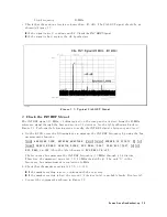
Reviews: