At
the
end
of
the
test,
the
analyzer
is
set
to
the
power-on
default
state
because
the
data
in
the
tested
memories
is
destroyed.
During
this
test,
a
test
pattern
is
written
into
the
memories
and
then
the
pattern
is
read
back
and
checked.
If
the
test
fails
,
the
test
displays
an
error
message
for
a
few
seconds
and
then
sets
the
analyzer
to
the
default
state
.
The
error
message
indicates
the
faulty
memory
.
3:
A51
GSP
Runs
only
when
selected.
It
veries
the
following
circuit
blocks
on
the
A51
GSP:
GSP
Chip
DRAM
VRAM
When
this
test
starts
,
4
Ch
1
5
LED
and
4
Ch
2
5
LED
are
turned
o.
At
the
end
of
this
test,
the
analyzer
is
set
to
the
power-on
default
state
because
the
data
in
the
tested
memories
is
destroyed.
During
this
test,
a
test
pattern
is
written
into
the
memories
and
then
the
pattern
is
read
back
and
checked.
If
the
test
fails
,
the
test
indicates
the
faulty
circuit
using
the
4
Ch
1
5
LED
,
the
4
Ch
2
5
LED
,
and
beeps
.
It
then
sets
the
analyzer
to
the
default
state
.
If
the
GSP
chip
is
faulty
,
a
beep
sounds
and
the
LEDs
blink
once
.
If
the
DRAM
is
faulty
,
two
beeps
sound
and
the
LEDs
blink
twice
.
If
the
VRAM
is
faulty
,
three
beeps
sound
and
the
LEDs
blink
three
times
.
4:
A2
POST
REGULA
TOR
V
eries
all
A2
post
regulator
output
voltages:
+5
V(A
UX),
+15
V(A
UX)
015
V
,
012.6
V
,
05
V
,
+5
V
,
+5.3
V
,
+8.5
V
,
+15
V
,
+22
V
,
F
AN
POWER,
GND
This
test
measures
the
A2
output
voltages
at
DC
bus
nodes
1
through
12,
and
26.
It
checks
that
each
measured
value
is
within
limits
.
5:
A6
A/D
CONVERTER
V
eries
the
following
circuit
blocks
on
the
A6
Receiver
IF:
A/D
Converter
Gain
Y
Gain
Z
Range
R
This
test
measures
the
A/D
converter's
reference
voltage
(VREF)
at
DC
bus
node
25
through
the
gain
Y
,
the
gain
Z,
and
the
range
R.
These
circuits
are
set
to
several
settings
in
the
test.
F
or
each
setting,
this
test
checks
that
the
measured
value
is
within
limits
.
6:
A5
REFERENCE
OSC
V
eries
the
reference
oscillator
in
the
A5
synthesizer
.
This
test
measures
the
V
CO
tuning
voltage
at
DC
bus
node
22
and
the
frequency
(2.5
MHz)
at
frequency
bus
node
6.
It
then
checks
that
each
measured
value
is
within
limits
.
7:
A5
FRA
CTIONAL
N
OSC
V
eries
the
fractional
N
oscillator
in
the
A5
synthesizer
.
This
sets
the
oscillator
frequency
to
several
frequencies
over
the
entire
range
.
F
or
each
setting,
this
test
measures
the
V
CO
tuning
voltage
at
DC
bus
node
20
and
the
frequency
at
frequency
bus
node
4.
It
then
checks
that
each
measured
value
is
within
limits
.
10-8
Service
K
ey
Menus
Summary of Contents for Agilent 4396B
Page 10: ......
Page 32: ......
Page 43: ...Figure 2 7 CAL OUT Level Adjustment Location Adjustments and Correction Constants 2 11 ...
Page 46: ...Figure 2 10 Comb Generator Output 2 14 Adjustments and Correction Constants ...
Page 62: ...Figure 2 26 Final Gain Adjustment Location 2 30 Adjustments and Correction Constants ...
Page 76: ...Figure 3 1 Troubleshooting Organization 3 2 T roubleshooting ...
Page 84: ......
Page 90: ...Figure 5 1 Power Supply Lines Simpli ed Block Diagram 5 2 Power Supply T roubleshooting ...
Page 107: ...Figure 5 12 Power Supply Block Diagram 1 Power Supply T roubleshooting 5 19 ...
Page 108: ...Figure 5 13 Power Supply Block Diagram 2 5 20 Power Supply T roubleshooting ...
Page 109: ...Figure 5 14 Power Supply Block Diagram 3 Power Supply T roubleshooting 5 21 ...
Page 110: ......
Page 112: ...Figure 6 1 Digital Control Group Simpli ed Block Diagram 6 2 Digital Control T roubleshooting ...
Page 124: ......
Page 126: ...Figure 7 1 Source Group Block Diagram 7 2 Source Group T roubleshooting ...
Page 160: ...Figure 8 1 Receiver Group Simpli ed Block Diagram 8 2 Receiver Group T roubleshooting ...
Page 168: ......
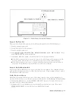
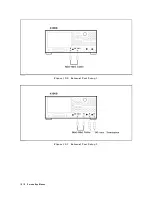
Page 184: ...Figure 10 6 External Test Setup 1 Figure 10 7 External Test Setup 2 10 10 Service Key Menus ...
Page 185: ...Figure 10 8 External Test Setup 3 Figure 10 9 External Test Setup 4 Service Key Menus 10 11 ...
Page 226: ...Figure 11 3 Power Supply Functional Group Simpli ed Block Diagram 11 6 Theory of Operation ...
Page 231: ...Figure 11 5 Digital Control Group Simpli ed Block Diagram Theory of Operation 11 11 ...
Page 235: ...Figure 11 6 Source Simpli ed Block Diagram Theory of Operation 11 15 ...
Page 244: ...Figure 11 7 Receiver Simpli ed Block Diagram 11 24 Theory of Operation ...
Page 249: ...Figure IDC5S11001 here Figure 11 8 4396B Source Group Block Diagram Theory of Operation 11 29 ...
Page 254: ...Figure 12 1 Top View Major Assemblies 12 4 Replaceable Parts ...
Page 290: ...Figure 12 36 Main Frame Assembly Parts 17 19 12 40 Replaceable Parts ...
Page 294: ......
Page 308: ......
Page 311: ...Figure C 1 Power Cable Supplied Power Requirement C 3 ...
Page 312: ......
Page 324: ......


