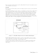
A1
CPU
The
A1
CPU
consists
of
the
following
circuits
and
parts
(See
Figure
11-5 ):
CPU
central
processing
unit
that
controls
the
analyzer
.
DSP
digital
signal
processor
that
is
used
for
fast
data
processing.
Memory
storages
consists
of
BOOT
ROMs
,
Flash
Memory
,
EEPROM,
Backup
SRAM,
DRAM,
and
Dual
P
ort
SRAM.
The
backup
SRAM
is
powered
from
a
large
capacitor
that
is
charged
when
the
analyzer
is
turned
on.
Therefore
,
the
SRAM
keeps
its
data
at
least
72
hours
after
the
analyzer
is
turned
o.
The
Dual
P
ort
SRAM
is
used
for
communication
between
the
CPU
and
DSP
.
F-Bus
Timer
is
used
in
the
frequency
bus
measurement
that
is
a
diagnostic
function
of
the
analyzer
.
F
or
a
description
of
the
frequency
bus
measurement,
see
the
Service
K
ey
Menus
chapter
.
Analog
Board
Interface
interfaces
between
the
CPU
and
analog
assemblies
A3
through
A9
Keyboard
Controller
controls
the
A30
front-panel
keyboard.
A
udio
Interface
controls
the
beeper
on
the
A30
front-panel
keyboard.
FDD
Control
controls
the
A53
FDD
.
GPIB
Control
communicates
with
the
external
GPIB
devices
through
the
GPIB
connector
on
the
A31
I/O
connector
.
S-P
ara
Control
controls
a
test
set
through
the
TEST
SET
I/O
INTERCONNECT
connector
on
the
A31
I/O
connector
.
External
Keyboard
Control
interfaces
between
the
CPU
and
the
external
keyboard
through
the
mini
DIN
connector
on
the
A32
I-B
ASIC
Interface
.
I/O
Control
controls
the
external
devices
through
the
I/O
PORT
connector
on
the
A32
IB
ASIC
interface
.
It
also
interfaces
between
the
CPU
and
the
external
inputs
through
the
EXT
PROG
RUN/CONT
connector
.
A30
Front-P
anel
K
eyboard
The
A30
front-panel
keyboard
assembly
detects
your
inputs
(key
inputs
and
RPG
inputs)
from
the
front
panel
of
the
analyzer
,
and
transmits
them
to
the
keyboard
controller
on
A1.
A31
I/O
Connector
The
two
A31
I/O
connectors
are
the
GPIB
connector
and
the
TEST
SET
I/O
INTERCONNECT
connector
.
These
connectors
are
connected
to
the
GPIB
controller
and
the
S-parameter
control
circuit
on
A1
through
the
A20
motherboard.
A32
I-B
ASIC
Interface
The
three
A32
I/O
connectors
are
the
EXT
PROG
RUN/CONT
connector
,
the
I/O
P
ort
connector
,
and
the
mini
DIN
Keyboard
connector
.
These
connectors
are
connected
to
the
I/O
control
and
mini
DIN
control
circuit
on
A1
through
the
A20
motherboard.
11-12
Theory
of
Operation
Summary of Contents for Agilent 4396B
Page 10: ......
Page 32: ......
Page 43: ...Figure 2 7 CAL OUT Level Adjustment Location Adjustments and Correction Constants 2 11 ...
Page 46: ...Figure 2 10 Comb Generator Output 2 14 Adjustments and Correction Constants ...
Page 62: ...Figure 2 26 Final Gain Adjustment Location 2 30 Adjustments and Correction Constants ...
Page 76: ...Figure 3 1 Troubleshooting Organization 3 2 T roubleshooting ...
Page 84: ......
Page 90: ...Figure 5 1 Power Supply Lines Simpli ed Block Diagram 5 2 Power Supply T roubleshooting ...
Page 107: ...Figure 5 12 Power Supply Block Diagram 1 Power Supply T roubleshooting 5 19 ...
Page 108: ...Figure 5 13 Power Supply Block Diagram 2 5 20 Power Supply T roubleshooting ...
Page 109: ...Figure 5 14 Power Supply Block Diagram 3 Power Supply T roubleshooting 5 21 ...
Page 110: ......
Page 112: ...Figure 6 1 Digital Control Group Simpli ed Block Diagram 6 2 Digital Control T roubleshooting ...
Page 124: ......
Page 126: ...Figure 7 1 Source Group Block Diagram 7 2 Source Group T roubleshooting ...
Page 160: ...Figure 8 1 Receiver Group Simpli ed Block Diagram 8 2 Receiver Group T roubleshooting ...
Page 168: ......
Page 184: ...Figure 10 6 External Test Setup 1 Figure 10 7 External Test Setup 2 10 10 Service Key Menus ...
Page 185: ...Figure 10 8 External Test Setup 3 Figure 10 9 External Test Setup 4 Service Key Menus 10 11 ...
Page 226: ...Figure 11 3 Power Supply Functional Group Simpli ed Block Diagram 11 6 Theory of Operation ...
Page 231: ...Figure 11 5 Digital Control Group Simpli ed Block Diagram Theory of Operation 11 11 ...
Page 235: ...Figure 11 6 Source Simpli ed Block Diagram Theory of Operation 11 15 ...
Page 244: ...Figure 11 7 Receiver Simpli ed Block Diagram 11 24 Theory of Operation ...
Page 249: ...Figure IDC5S11001 here Figure 11 8 4396B Source Group Block Diagram Theory of Operation 11 29 ...
Page 254: ...Figure 12 1 Top View Major Assemblies 12 4 Replaceable Parts ...
Page 290: ...Figure 12 36 Main Frame Assembly Parts 17 19 12 40 Replaceable Parts ...
Page 294: ......
Page 308: ......
Page 311: ...Figure C 1 Power Cable Supplied Power Requirement C 3 ...
Page 312: ......
Page 324: ......


