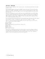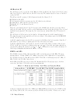
The
FRA
C
N
OSC
is
a
phase
locked
oscillator
.
The
output
signal
is
phase
locked
to
the
10
MHz
reference
signal
of
the
REF
OSC.
The
oscillator
contains
a
31.25
MHz
to
62.5
MHz
V
CO
,
a
phase
detector
,
and
a
fractional
N
divider
(N.F
.
divider:
1/integer
.fraction).
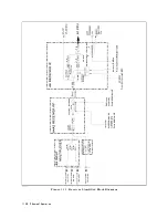
See
Figure
11-8.
The
10
MHz
reference
signal
from
the
REF
OSC
is
applied
to
the
phase
detector
through
the
1/10
divider
.
The
reference
signal
is
then
compared
with
the
V
CO
frequency
(F
vco
)
divided
by
the
fractional
N
divider
in
the
phase
detector
.
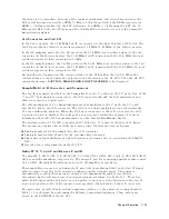
Phase
locking
imposes
the
condition
of
10
MHz/10
=
F
vco
/N.F
.
Therefore
,
the
output
frequency
(F
vco
)
is
locked
to
1
MHz
x
N.F
.
The
fractional
N
divider
is
a
dedicated
divider
used
to
generate
the
high
frequency
resolution
signal.
It
divides
the
signal
frequency
by
a
real
value
(N.F
.).
The
resolution
of
the
fractional
part
F
is
3.55
x
10
015
(=
1/2
48
).
Therefore
,
the
FRA
C
N
OSC
generates
a
swept
signal
with
3.55
nHz
(1
MHz
x
3.55
x
10
015
)
frequency
resolution.
The
fractional
N
divider
is
controlled
by
the
A1
CPU
and
the
A6
Receiver
IF
.
STEP
OSC
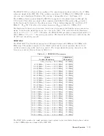
The
STEP
OSC
(Step
Oscillator)
generates
a
CW
signal
between
470
MHz
and
930
MHz
in
20
MHz
steps
.
The
signal
is
supplied
to
the
A4A1
1st
LO
and
is
used
to
generate
the
1st
local
oscillator
signal
(only
in
the
triple-loop
mode).
The
output
signal
frequency
depends
on
the
frequency
center
setting
as
shown
in
T
able
11-1.
T
able
11-1.
STEP
OSC
Frequency
4396B
Center
Frequency
STEP
OSC
Frequency
0
Hz
Center
<
48.92
MHz
470
MHz
48.92
MHz
Center
<
128.92
MHz
490
MHz
128.92
MHz
Center
<
208.92
MHz
510
MHz
208.92
MHz
Center
<
288.92
MHz
530
MHz
288.92
MHz
Center
<
368.92
MHz
550
MHz
368.92
MHz
Center
<
448.92
MHz
570
MHz
448.92
MHz
Center
<
528.92
MHz
590
MHz
528.92
MHz
Center
<
608.92
MHz
610
MHz
608.92
MHz
Center
<
688.92
MHz
630
MHz
688.92
MHz
Center
<
768.92
MHz
650
MHz
768.92
MHz
Center
<
848.92
MHz
670
MHz
848.92
MHz
Center
<
928.92
MHz
690
MHz
928.92
MHz
Center
<
1008.92
MHz
710
MHz
1008.92
MHz
Center
<
1088.92
MHz
730
MHz
1088.92
MHz
Center
<
1168.92
MHz
750
MHz
1168.92
MHz
Center
<
1248.92
MHz
770
MHz
1248.92
MHz
Center
<
1328.92
MHz
790
MHz
1328.92
MHz
Center
<
1408.92
MHz
810
MHz
1408.92
MHz
Center
<
1488.92
MHz
830
MHz
1488.92
MHz
Center
<
1568.92
MHz
850
MHz
1568.92
MHz
Center
<
1648.92
MHz
870
MHz
1648.92
MHz
Center
<
1728.92
MHz
890
MHz
1728.92
MHz
Center
<
1808.92
MHz
910
MHz
1808.92
MHz
Center
<
1820.00
MHz
930
MHz
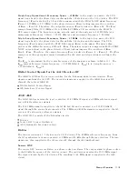
The
STEP
OSC
consists
of
a
comb
generator
and
a
phase
locked
oscillator
that
is
phase
locked
to
the
10
MHz
reference
signal
of
the
REF
OSC.
Theory
of
Operation
11-17
Summary of Contents for Agilent 4396B
Page 10: ......
Page 32: ......
Page 43: ...Figure 2 7 CAL OUT Level Adjustment Location Adjustments and Correction Constants 2 11 ...
Page 46: ...Figure 2 10 Comb Generator Output 2 14 Adjustments and Correction Constants ...
Page 62: ...Figure 2 26 Final Gain Adjustment Location 2 30 Adjustments and Correction Constants ...
Page 76: ...Figure 3 1 Troubleshooting Organization 3 2 T roubleshooting ...
Page 84: ......
Page 90: ...Figure 5 1 Power Supply Lines Simpli ed Block Diagram 5 2 Power Supply T roubleshooting ...
Page 107: ...Figure 5 12 Power Supply Block Diagram 1 Power Supply T roubleshooting 5 19 ...
Page 108: ...Figure 5 13 Power Supply Block Diagram 2 5 20 Power Supply T roubleshooting ...
Page 109: ...Figure 5 14 Power Supply Block Diagram 3 Power Supply T roubleshooting 5 21 ...
Page 110: ......
Page 112: ...Figure 6 1 Digital Control Group Simpli ed Block Diagram 6 2 Digital Control T roubleshooting ...
Page 124: ......
Page 126: ...Figure 7 1 Source Group Block Diagram 7 2 Source Group T roubleshooting ...
Page 160: ...Figure 8 1 Receiver Group Simpli ed Block Diagram 8 2 Receiver Group T roubleshooting ...
Page 168: ......
Page 184: ...Figure 10 6 External Test Setup 1 Figure 10 7 External Test Setup 2 10 10 Service Key Menus ...
Page 185: ...Figure 10 8 External Test Setup 3 Figure 10 9 External Test Setup 4 Service Key Menus 10 11 ...
Page 226: ...Figure 11 3 Power Supply Functional Group Simpli ed Block Diagram 11 6 Theory of Operation ...
Page 231: ...Figure 11 5 Digital Control Group Simpli ed Block Diagram Theory of Operation 11 11 ...
Page 235: ...Figure 11 6 Source Simpli ed Block Diagram Theory of Operation 11 15 ...
Page 244: ...Figure 11 7 Receiver Simpli ed Block Diagram 11 24 Theory of Operation ...
Page 249: ...Figure IDC5S11001 here Figure 11 8 4396B Source Group Block Diagram Theory of Operation 11 29 ...
Page 254: ...Figure 12 1 Top View Major Assemblies 12 4 Replaceable Parts ...
Page 290: ...Figure 12 36 Main Frame Assembly Parts 17 19 12 40 Replaceable Parts ...
Page 294: ......
Page 308: ......
Page 311: ...Figure C 1 Power Cable Supplied Power Requirement C 3 ...
Page 312: ......
Page 324: ......

