A6
Receiver
IF
The
A6
Receiver
IF
converts
the
21.42
MHz
2nd
IF
from
A4A2
to
the
nal
3rd
IF
.
The
3rd
IF
is
then
converted
to
a
digital
value
in
the
A/D
converter
.
The
digital
signal
is
routed
to
the
DSP
on
the
A1
CPU
.
The
A6
receiver
IF
consists
of
the
following
circuits
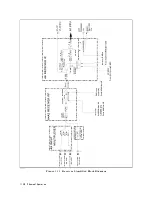
(See
Figure
11-7):
IF
BPFs
and
IF
LPFs
3rd
Converter
(third
converter)
and
3rd
LO
(third
local
oscillator)
Sample/Hold,
A/D
Converter
,
and
Sequencer
Gains
W
,
X,
Y
,
Z
and
Ranges
F
and
R
Sequence
There
are
two
signal
paths
(0
and
90
)
between
the
IF
BPFs
and
the
A/D
converter
.
These
paths
are
the
same
and
are
used
for
a
DC
sampling
mode
that
is
described
below
.
The
3rd
local
oscillator
input
signals
to
the
respective
3rd
converters
are
phase
shifted
by
90
from
each
other
.
The
A6
Receiver
IF
has
two
operation
modes
,
A
C
sampling
mode
and
DC
sampling
mode
.
The
sampling
mode
is
automatically
selected
according
to
the
analyzer
mode
and
IFBW/RBW
setting.
See
the
T
able
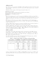
11-4 .
In
the
A
C
sampling
mode
,
the
2nd
IF
is
converted
to
20
kHz
in
the
3rd
converter
.
Only
the
0
path
signal
is
converted
to
a
digital
value
and
used
for
data
processing.
In
the
DC
sampling
mode
,
the
2nd
IF
is
converted
to
DC
in
the
third
converter
.
The
0
and
90
DC
3rd
IF
are
converted
to
digital
values
(e
0
and
e
90
).
Then
the
spectrum
amplitude
is
calculated
by
taking
the
square
root
of
e
0
2
+
e
90
2
.
This
mode
is
used
to
take
advantage
of
the
fast
spectrum
measurement
with
RBWs
10
kHz.
IF
BPFs
and
LPFs
The
IF
BPFs
consist
of
three
bandpass
lter
with
a
enter
frequency
21.42
MHz.
The
pass
bandwidths
are
10
kHz,
1
MHz,
and
3
MHz,
respectively
.
The
10
kHz
BPF
is
a
crystal
BPF
.
The
IF
LPFs
consist
of
a
through
and
four
LPFs
.
The
LPFs'
cuto
frequencies
are
5
kHz,
15
kHz,
50
kHz,
and
150
kHz,
respectively
.
These
BPFs
and
LPFs
are
used
to
shape
the
bandwidth
of
the
IF
signals
going
to
the
A/D
converter
.
See
T
able
11-4
for
the
selection
requirements
.
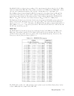
T
able
11-4.
Measurement
Setting,
Used
Filter
,
and
Sampling
Mode
Analyzer
Mode
IF
B
W/RB
W
Used
IF
BPF
Used
IF
LPF
Sampling
Mode
Network
Analyzer
10
kHz,
40
kHz
1
MHz
50
kHz
A
C
Sampling
10
Hz
to
3
kHz
10
kHz
(X'tal)
50
kHz
A
C
Sampling
Spectrum
Analyzer
3
MHz
3
MHz
Through
DC
Sampling
1
MHz
1
MHz
Through
DC
Sampling
300
kHz
1
MHz
150
kHz
DC
Sampling
100
kHz
1
MHz
50
kHz
DC
Sampling
30
kHz
1
MHz
15
kHz
DC
Sampling
10
kHz
1
MHz
5
kHz
DC
Sampling
1
Hz
to
3
kHz
10
kHz
(X'tal)
50
kHz
A
C
Sampling
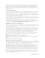
In
the
spectrum
measurement,
the
3
MHz
and
1
MHz
RBWs
are
shaped
by
the
IF
BPFs
at
the
2nd
IF
stage
(before
the
3rd
converter)
and
the
IF
LPFs
are
by-passed.
This
is
done
so
that
11-26
Theory
of
Operation
Summary of Contents for Agilent 4396B
Page 10: ......
Page 32: ......
Page 43: ...Figure 2 7 CAL OUT Level Adjustment Location Adjustments and Correction Constants 2 11 ...
Page 46: ...Figure 2 10 Comb Generator Output 2 14 Adjustments and Correction Constants ...
Page 62: ...Figure 2 26 Final Gain Adjustment Location 2 30 Adjustments and Correction Constants ...
Page 76: ...Figure 3 1 Troubleshooting Organization 3 2 T roubleshooting ...
Page 84: ......
Page 90: ...Figure 5 1 Power Supply Lines Simpli ed Block Diagram 5 2 Power Supply T roubleshooting ...
Page 107: ...Figure 5 12 Power Supply Block Diagram 1 Power Supply T roubleshooting 5 19 ...
Page 108: ...Figure 5 13 Power Supply Block Diagram 2 5 20 Power Supply T roubleshooting ...
Page 109: ...Figure 5 14 Power Supply Block Diagram 3 Power Supply T roubleshooting 5 21 ...
Page 110: ......
Page 112: ...Figure 6 1 Digital Control Group Simpli ed Block Diagram 6 2 Digital Control T roubleshooting ...
Page 124: ......
Page 126: ...Figure 7 1 Source Group Block Diagram 7 2 Source Group T roubleshooting ...
Page 160: ...Figure 8 1 Receiver Group Simpli ed Block Diagram 8 2 Receiver Group T roubleshooting ...
Page 168: ......
Page 184: ...Figure 10 6 External Test Setup 1 Figure 10 7 External Test Setup 2 10 10 Service Key Menus ...
Page 185: ...Figure 10 8 External Test Setup 3 Figure 10 9 External Test Setup 4 Service Key Menus 10 11 ...
Page 226: ...Figure 11 3 Power Supply Functional Group Simpli ed Block Diagram 11 6 Theory of Operation ...
Page 231: ...Figure 11 5 Digital Control Group Simpli ed Block Diagram Theory of Operation 11 11 ...
Page 235: ...Figure 11 6 Source Simpli ed Block Diagram Theory of Operation 11 15 ...
Page 244: ...Figure 11 7 Receiver Simpli ed Block Diagram 11 24 Theory of Operation ...
Page 249: ...Figure IDC5S11001 here Figure 11 8 4396B Source Group Block Diagram Theory of Operation 11 29 ...
Page 254: ...Figure 12 1 Top View Major Assemblies 12 4 Replaceable Parts ...
Page 290: ...Figure 12 36 Main Frame Assembly Parts 17 19 12 40 Replaceable Parts ...
Page 294: ......
Page 308: ......
Page 311: ...Figure C 1 Power Cable Supplied Power Requirement C 3 ...
Page 312: ......
Page 324: ......


