194
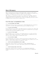
EEPROM
WRITE
ERROR
Data
cannot
be
stored
properly
into
the
EEPROM
on
the
A1
CPU
.
This
message
is
displayed
when
performing
the
display
background
adjustment
or
updating
correction
constants
in
the
EEPROM
using
the
adjustment
program.
Troubleshoot
the
A1
CPU
in
accordance
with
the
Digital
Control
Troubleshooting
chapter
.
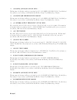
200
F-BUS
TIMER
CHIP
TEST
F
AILED
The
A1
CPU's
F-BUS
(Frequency
Bus)
timer
does
not
work
properly
.
This
message
is
displayed
when
an
internal
test
1:
A1
CPU
fails
.
Replace
the
A1
CPU
with
a
new
one
.
See
the
Digital
Control
Troubleshooting
chapter
.
213
F
AILURE
FOUND
FROM
A/D
MUX
TO
A/D
CONVERTER
A
trouble
is
found
on
the
signal
path
from
the
A/D
multiplexer
to
A/D
converter
on
the
A6
receiver
IF
.
This
message
is
displayed
when
an
internal
test
5:
A6
A/D
CONVERTER
fails
.
Troubleshoot
the
A6
receiver
IF
in
accordance
with
the
R
eceiver
Troubleshooting
chapter
.
212
F
AN
PO
WER
OUT
OF
SPEC
The
voltage
of
the
fan
power
supply
at
the
DC
bus
node
11
is
out
of
its
limits
.
This
message
is
displayed
when
an
internal
test
4:
A2
POST
REGULA
TOR
fails
.
Troubleshoot
the
power
supply
functional
group
in
accordance
with
the
P
ower
Supply
Troubleshooting
chapter
.
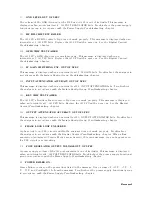
203
FDC
CHIP
TEST
F
AILED
The
A1
CPU's
FDC
(Flexible
Disk
drive
control)
chip
does
not
work
properly
.
This
message
is
displayed
when
an
internal
test
1:
A1
CPU
fails
.
Replace
the
A1
CPU
with
a
new
one
.
See
the
Digital
Control
Troubleshooting
chapter
.
196
FLASH
MEMORY
CHECK
SUM
ERROR
The
data
(Firmware)
stored
in
the
A1
ash
memory
are
invalid.
This
message
is
displayed
in
the
bootloader
menu.
Troubleshoot
the
A1
CPU
in
accordance
with
the
Digital
Control
Troubleshooting
chapter
.
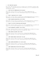
226
FLOPPY
DISK
DRIVE
F
AILURE
FOUND
The
A53
built-in
FDD
(oppy
disk
drive)
does
not
work
properly
.
This
message
is
displayed
when
an
external
test
18:
DSK
DR
F
A
UL
T
ISOL'N
fails
.
Replace
the
A53
FDD
with
a
new
one
.
See
the
Digital
Control
Troubleshooting
chapter
.
236
FRA
CTION
SPURIOUS
OUT
OF
SPEC
This
message
is
displayed
when
an
external
test
27:
FRA
CTION
SPURIOUS
fails
.
Troubleshoot
the
analyzer
in
accordance
with
the
Isolate
F
aulty
Group
Troubleshooting
chapter
.
215
FRA
CTIONAL
N
OSC
TEST
F
AILED
The
fractional
N
oscillator
on
the
A5
synthesizer
does
not
work
properly
.
This
message
is
displayed
when
an
internal
test
7:
A5
FRA
CTIONAL
N
OSC
fails
.
Troubleshoot
the
source
group
in
accordance
with
the
Source
Troubleshooting
chapter
.
Messages-4
Summary of Contents for Agilent 4396B
Page 10: ......
Page 32: ......
Page 43: ...Figure 2 7 CAL OUT Level Adjustment Location Adjustments and Correction Constants 2 11 ...
Page 46: ...Figure 2 10 Comb Generator Output 2 14 Adjustments and Correction Constants ...
Page 62: ...Figure 2 26 Final Gain Adjustment Location 2 30 Adjustments and Correction Constants ...
Page 76: ...Figure 3 1 Troubleshooting Organization 3 2 T roubleshooting ...
Page 84: ......
Page 90: ...Figure 5 1 Power Supply Lines Simpli ed Block Diagram 5 2 Power Supply T roubleshooting ...
Page 107: ...Figure 5 12 Power Supply Block Diagram 1 Power Supply T roubleshooting 5 19 ...
Page 108: ...Figure 5 13 Power Supply Block Diagram 2 5 20 Power Supply T roubleshooting ...
Page 109: ...Figure 5 14 Power Supply Block Diagram 3 Power Supply T roubleshooting 5 21 ...
Page 110: ......
Page 112: ...Figure 6 1 Digital Control Group Simpli ed Block Diagram 6 2 Digital Control T roubleshooting ...
Page 124: ......
Page 126: ...Figure 7 1 Source Group Block Diagram 7 2 Source Group T roubleshooting ...
Page 160: ...Figure 8 1 Receiver Group Simpli ed Block Diagram 8 2 Receiver Group T roubleshooting ...
Page 168: ......
Page 184: ...Figure 10 6 External Test Setup 1 Figure 10 7 External Test Setup 2 10 10 Service Key Menus ...
Page 185: ...Figure 10 8 External Test Setup 3 Figure 10 9 External Test Setup 4 Service Key Menus 10 11 ...
Page 226: ...Figure 11 3 Power Supply Functional Group Simpli ed Block Diagram 11 6 Theory of Operation ...
Page 231: ...Figure 11 5 Digital Control Group Simpli ed Block Diagram Theory of Operation 11 11 ...
Page 235: ...Figure 11 6 Source Simpli ed Block Diagram Theory of Operation 11 15 ...
Page 244: ...Figure 11 7 Receiver Simpli ed Block Diagram 11 24 Theory of Operation ...
Page 249: ...Figure IDC5S11001 here Figure 11 8 4396B Source Group Block Diagram Theory of Operation 11 29 ...
Page 254: ...Figure 12 1 Top View Major Assemblies 12 4 Replaceable Parts ...
Page 290: ...Figure 12 36 Main Frame Assembly Parts 17 19 12 40 Replaceable Parts ...
Page 294: ......
Page 308: ......
Page 311: ...Figure C 1 Power Cable Supplied Power Requirement C 3 ...
Page 312: ......
Page 324: ......


