background image


E2730A VXI RF TUNER 


3-10 

OPERATION 

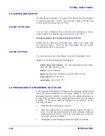
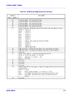
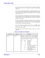
Table 3-3.  Reference Selection 


Command 

Response 

Description 

REF nrf 


Set Reference to Internal or External 
0 = Internal  Reference 
1= VXI Bus Reference  
2 = External Reference 

REF? 

REF nr1 

Request Reference Setting 
Reset: REF 0 
Example: REF 1 


RESET 


The *RST command returns all tuner parameters to their reset values (the 
same values which occur at power up).  The reset command does not affect 
the contents of channel memory or SRQ registers.  The commands in this 
message category are listed in 

Table 3-4.


Table 3-4.  Reset 


Command 

Response 

Description 

*RST 


Set all tuner device messages to the reset values. 


MEMORY CLEAR 


The memory clear  (CLM) command allows clearing of channel storage 
memory.  If the CLM 1 command is sent, storage memory will be cleared.  
The command in this message category is listed in 

Table 3-5


Table 3-5.  Memory Clear 


Command 

Response 

Description 

CLM nrf 


Clear channel storage memory. 
nrf              Description 
 1         Clear channel storage memory 


Summary of Contents for E2730A

Page 1: ...子計測事業はキーサイト テクノロジーとなりま した この文書はお客様に製品のサポートをご提供するために公開しておりますが アジレ ント の記載が残り 会社名等は最新の情報に更新されていません 詳細は www keysight co jp をご覧ください 訂正のお願い 1999 年 ヒューレット パッカードの電子計測事業はアジレント テクノロジーの一事業とな り 2014 年 8 月にはキーサイト テクノロジーとなりました この文書はお客様に製品のサポ ートをご提供するために公開しておりますが アジレント または ヒューレット パッカ ード 横河ヒューレット パッカード の記載が残り 会社名等は最新の情報に更新され ていません 詳細は www keysight co jp をご覧ください ...

Page 2: ...INSTALLATION AND OPERATION MANUAL FOR THE AGILENT TECHNOLOGIES E2730A VXI RF TUNER P N 181629 003 Revision C Copyright BAE SYSTEMS 2002 All Rights Reserved JUNE 2002 ...

Page 3: ...ions EAR of the United States Diversion contrary to U S law is prohibited SAFETY NOTICES CAUTION A CAUTION notice denotes a hazard It calls attention to an operating procedure practice or the like that if not correctly performed or adhered to could result in damage to the product or loss of important data Do not proceed beyond a CAUTION notice until the indicated conditions are fully understood an...

Page 4: ...nk C vii thru x Table of Contents C 1 i Section Cover C 1 ii Intentionally Blank C 1 1 thru 1 4 Section One Pages C 2 ii Intentionally Blank C 2 1 thru 2 12 Section Two Pages C 3 i Section Cover C 3 ii Intentionally Blank C 3 1 thru 3 32 Section Three Pages C 4 i Section Cover C 4 ii Intentionally Blank C 4 1 thru 4 4 Section Four Pages C FP i Foldouts Cover Page C FP ii Intentionally Blank C FP 1...

Page 5: ...E2730A VXI RF TUNER iv LIST OF EFFECTIVE PAGES THIS PAGE INTENTIONALLY LEFT BLANK ...

Page 6: ...E2730A VXI RF TUNER REVISION RECORD v E2730A VXI RF TUNER INSTALLATION AND OPERATION MANUAL REVISION RECORD Revision Description Date C Production Release 6 2002 ...

Page 7: ...E2730A VXI RF TUNER vi REVISION RECORD THIS PAGE INTENTIONALLY LEFT BLANK ...

Page 8: ...2 2 Connector Signals 2 1 2 2 1 VXI P1 Standard VXIbus P1 A1P1 2 4 2 2 2 VXI P1 Standard VXIbus P2 A1P2 2 5 2 2 3 AUX Auxiliary RS 232 Control Connector A5J2 2 6 2 2 4 RF IN J2 2 6 2 2 5 10 MHz EXT REF J8 2 6 2 2 6 70 MHz IF OUT W4J4 2 7 2 2 7 2nd LO IN OUT W3J3 2 7 2 2 8 1st LO IN OUT W1J1 2 7 2 3 Power and Cooling Requirements Versus Mainframe Selection 2 8 2 4 Setting the E2730A s Logical Addre...

Page 9: ...n Protocol 3 4 Word Serial IEEE 488 2 Commands 3 4 Register Based VXI Operations 3 6 3 3 5 Interrupters 3 8 3 4 Tuner Operations 3 9 3 4 1 Setup Operations 3 9 Reference Selection 3 9 Reset 3 10 Memory Clear 3 10 3 4 2 Manual Control 3 11 Frequency Operations 3 11 Tuner Attenuation Operations 3 12 3 4 3 Memory Operation 3 13 Direct Memory Comments 3 13 Store and Recall Operations 3 14 3 4 4 Commun...

Page 10: ... 2 4 Pin Assignments of the Standard VXIbus P1 Connector 2 5 2 5 Agilent Call Centers MD Regional Headquarters 2 12 3 1 Word Serial Commands 3 2 3 2 VXI Memory Register Based Commands 3 7 3 3 Reference Selection 3 10 3 4 Reset 3 10 3 5 Memory Clear 3 10 3 6 Frequency Operations 3 12 3 7 Tuner Attenuation 3 12 3 8 Direct Memory Commands 3 14 3 9 Store and Recall Operations 3 15 3 10 Communications ...

Page 11: ...xternal Connectors and Indicators 2 3 2 2 AUX Connector Pin Assignments 2 6 2 3 Setting the E2730A s Logical Address 2 9 2 4 E2730A Properly Installed in a Vertical Mainframe 2 10 3 1 E2730A SRQ Structure Diagram 3 18 FOLDOUTS Foldout Page FO 1 Type E2730A VXI RF Tuner Main Chassis Schematic Diagram 484331 2 Sheets FP 1 ...

Page 12: ...1 i SECTION 1 GENERAL DESCRIPTION ...

Page 13: ...1 ii THIS PAGE INTENTIONALLY LEFT BLANK ...

Page 14: ...e lock status of the Local Oscillator loops LOs contained in the tuner module The E2730A is operated remotely via a VXI interface or an RS 232 port located on the front panel By placing the tuner directly on a standard instrumentation and computing bus system integration is simplified and enhanced All functions are accessible via the VXI interface except for power on off control All data is passed...

Page 15: ... a plug in YIG Assembly The modules are attached to a milled out aluminum housing that makes up the main chassis POWER REQUIREMENTS 24V 0 0 Cooling 14 deg C rise ATTENTION o Front Panel fasteners must be secured to insure proper operation 6 V Stdby 24V 0 05A 0 05A 12V 0 11A 0 10A 12V 0 86A 0 15A 2V 0 03A 0 5 2V 0 40A 0 05A 5V 2 2A 0 05A DC Voltage DC Current Dynamic Current Manufacturer Code OxFFF...

Page 16: ...ximum Gain Control Modes Manual 56 dB range with 2 dB steps typical Image Rejection 90 dB IF Rejection 90 dB Phase Noise Better than 97 dBc Hz 20 kHz offset Typically 115 dBc Hz 100 kHz offset F1 to F2 Sweep Time 36 MHz step 5 0 msec max per sweep point with 1 kHz resolution LO Level at RF Input 90 dBm maximum Internally Generated Spurious 110 dBm equivalent RF input maximum VXI Interface Device T...

Page 17: ...ers uninstalled boards It changed identity information to Agilent Technologies E2730A In addition the CDT and CSN commands also changed format to comply with customer requests The YIG calibration routine has been enhanced to help the test technicians calibrate more units on the first try The code no longer allows access to the low level attenuators ATR and ATI via the binary command interface The ...

Page 18: ...2 i SECTION 2 INSTALLATION ...

Page 19: ...2 ii THIS PAGE INTENTIONALLY LEFT BLANK ...

Page 20: ...ndicators or connectors or any other signs of physical abuse or careless handling If damage is found forward an immediate request to the delivering carrier to perform an inspection and prepare a concealed damage report Do not destroy any packing material until it has been examined by an agent of the carrier Concurrently report the nature and extent of damage to your Customer Engineeer through your...

Page 21: ...A 1st Local Oscillator Bi directional Input Output Table 2 2 List of Mating Connectors Connector Type Ref Des Mating Connector CAGE Code Comment VXI P1 A1P1 VXI Interface Frame Not Supplied VXI P2 A1P2 VXI Interface Frame Not Supplied AUX 9 pin Micro D A5J2 MDSM 9SC Z11 71468 P O Accessory Kit RF IN SMA female J2 SMA male 9001 9023 005 19505 Not Supplied 10 MHz EXT REF SMA female J8 SMA male 9001 ...

Page 22: ...VXI RF TUNER INSTALLATION 2 3 ROW C PIN 1 ROW C PIN 1 ROW B PIN 1 ROW A PIN 1 A1P2 A1P1 ROW A PIN 1 ROW B PIN 1 PIN 32 ALL ROWS PIN 32 ALL ROWS 99 0087 Figure 2 1 Location of External Connectors and Indicators ...

Page 23: ...ls Row B Signals Row C Signals 1 2 3 4 5 6 7 8 9 10 11 12 13 14 15 16 17 18 19 20 21 22 23 24 25 26 27 28 29 30 31 32 D00 D01 D02 D03 D04 D05 D06 D07 GND SYSCLK GND DS1 DS0 WRITE GND DTACK GND AS GND IACK IACKIN IACKOUT AM4 A07 A06 A05 A04 A03 A02 A01 12V 5V BBSY BCLR ACFAIL BG0IN BG0OUT BG1IN BG1OUT BG2IN BG2OUT BG3IN BG3OUT BR0 BR1 BR2 BR3 AM0 AM1 AM2 AM3 GND not connected not connected GND IRQ7...

Page 24: ... 3 4 5 6 7 8 9 10 11 12 13 ECLTRG0 2V ECLTRG1 GND LBUSA00 LBUSA01 5 2V LBUSA02 LBUSA03 GND LBUSA04 LBUSA05 5 2V 5V GND RSV1 A24 A25 A26 A27 A28 A29 A30 A31 GND 5V CLK10 CLK10 GND 5 2V LBUSC00 LBUSC01 GND LBUSC02 LBUSC03 GND LBUSC04 LBUSC05 2V 14 15 16 17 18 19 20 21 22 23 24 25 26 27 28 29 30 31 32 LBUSA06 LBUSA07 GND LBUSA08 LBUSA09 5 2V LBUSA10 LBUSA11 GND TTLTRG0 TTLTRG2 5V TTLTRG4 TTLTRG6 GND ...

Page 25: ...in Assignments 2 2 4 RF IN J2 The RF IN SMA connector accepts 20 to 2700 MHz RF input signals from the antenna Nominal input impedance is 50 ohms Maximum RF input without incurring damage is a maximum of 100 milliwatts 2 2 5 10 MHz EXT REF J8 The 10 MHz EXT REF SMA connector accepts an input from an external reference source for use as the tuner s time base It accepts an input signal frequency of ...

Page 26: ...emi rigid RF cables between the LO inputs and outputs When the tuner is not used in master slave mode these cables must be disconnected to prevent spurious signals from appearing in both tuners Also an unused LO IN OUT connector should be terminated with mating termination dust cap MP2 2 2 8 1st LO IN OUT W1J1 The 1st LO IN OUT SMA bi directional connector provides a sample of the 1st LO synthesiz...

Page 27: ...SETTING THE E2730A s LOGICAL ADDRESS All modules in a VXI system must be assigned a logical address to allow controller to device communications The E2730A is assigned a logical address via either of two methods Dynamic Configuration DC or Static Configuration SC Refer to Section F in the VXIbus specification for details on these configurations The tuner is set to either DC or SC configurations by...

Page 28: ...onfigure the switch to provide this address PUSH THIS SIDE DOWN FOR LOGIC 0 PUSH THIS SIDE DOWN FOR LOGIC 1 SHOWN AT DEFAULT SETTING OF LOGICAL ADDRESS 255 LOGICAL ADDRESS SWITCH A1S1 1 2 3 4 5 6 7 8 NO DC COVER 97 0205 PUSH THIS SIDE DOWN FOR LOGIC 1 PUSH THIS SIDE DOWN FOR LOGIC 0 DO NOT TOUCH CONNECTOR CONTACTS DO NOT TOUCH CONNECTOR CONTACTS ON 1 SWITCH 3 7 6 5 4 2 8 SHOWN AT DEFAULT SETTING O...

Page 29: ... module installation instructions Refer also to the VXIbus Specification for proper module installation procedures and details on configuring the interrupt daisy chain on the mainframe backplane to bypass empty slots if required When installing the tuner in a vertical mainframe slide it in the appropriate module slot any slot except 0 with the RF IN SMA connector towards the top and the 3rd LO IN ...

Page 30: ...gnal which is available on the CLK10 and CLK10 lines To utilize the VXI 10 MHz reference each tuner must be remotely set to the VXI Bus Reference mode of operation via the REF command as explained in Section 3 Optionally an external 10 MHz reference signal may be applied to the Slot 0 Controller and then distributed to each tuner via the VXI bus NOTE The 10 MHz reference generated within the slot ...

Page 31: ...ates and Canada Test and Measurement Call Center 800 452 4844 toll free in US Europe 41 22 780 8111 Japan Measurement Assistance Center 81 0426 56 7832 Latin America 305 269 7548 Asia Pacific 85 22 599 7777 2 9 PREPARATION FOR RESHIPMENT OR STORAGE If the unit must be prepared for reshipment the packaging method should follow the pattern established in the original shipment Use the best packaging ...

Page 32: ...3 i SECTION 3 OPERATION ...

Page 33: ...3 ii THIS PAGE INTENTIONALLY LEFT BLANK ...

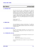
Page 34: ...y of the VXIbus Specification can be requested by writing to VXIbus Consortium Inc P O Box 1736 Vancouver WA 98668 U S A 3 2 INDICATORS All tuner indicators are located on the front panel Two LEDs are provided for monitoring the operating status of the unit The following paragraphs further explain the function of each LED The E2730A has no front panel controls 3 2 1 RUN INDICATOR GREEN LED This gr...

Page 35: ... queries are transferred to the VXIbus in response to the Word Serial Byte commands Table 3 1 Word Serial Commands Command Description Abort Normal Operation Causes device to cease normal operation Device returns to its default configuration aborting all operations Begin Normal Operation Notifies device that it can begin normal operation Byte Available Used to send a byte of data from a Commander ...

Page 36: ... routine The E2730A contains an offset register that can be written to by the resource manager to define its address Refer to Section F in the VXIbus Specification for further details on dynamic configurations If the switch is set for static configuration 1 254 the Resource Manager reads and acknowledges the set address 3 3 3 E2730A CONFIGURATION REGISTERS At startup it is the responsibility of th...

Page 37: ...th exceptions being communication protocol characters The parser accepts numeric arguments in the forgiving numeric representation form described below Multiple commands must be separated by the character Multiple arguments of a single command must be delimited with character s Message strings sent to the tuner must be terminated with a linefeed 0A hex character or VXI END COMMAND MESSAGE PROCESSI...

Page 38: ...th one restriction at least one digit must be present within the active data element 1 Plus or minus sign 2 Any number of digits up to eight 3 Decimal point 4 Any number of digits up to eight 5 Uppercase or lower case E e followed by an optional sign and at least one digit but no more than three digits This format specifies all numeric input data If the unit receives an nrf argument of a precision...

Page 39: ...e binary commands allow higher speed operation than the word serial operations They require less data transfer time and parsing than the word serial commands To optimize performance there is a minimum of error checking with the binary commands and it is the responsibility of the user s application to not send invalid binary commands to the tuner The E2730A has the ability to accept VXI commands vi...

Page 40: ...Command 1 Bit ATN PAM Bit 3 Not Used Bit 2 Not Used Bit 1 Not Used Bit 0 FRQ Command Bit 2C FRQ_HI_DATA High Word of Frequency long word 10 Hz resolution 2E FRQ_LO_DATA Low Word of Frequency long word 10 Hz resolution 30 Not Used 32 MAN_ATTN_DATA_1 Manual Attenuation Data Word 1 Bit 15 9 ATN Value Range 0 120 dB Bit 8 PAM Mode 0 OFF 1 ON Bit 7 0 Not Used 34 Not Used 36 Not Used 38 Not Used 3A Not ...

Page 41: ...low 1 FRQ 2 Manual Attenuation 2 1 ATN 2 2 PAM The frequency command is processed first because it takes the longest to complete After the tuner has processed one of the commands the corresponding bit in the binary command register is cleared The application must wait until all the bits in the binary command have been cleared before issuing another set of commands However the application may take ...

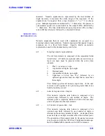
Page 42: ... Factory Configuration Maintenance 3 4 1 SETUP OPERATIONS Tuner Setup Operations are global commands that affect the E2730A regardless of the current operational mode These commands include external reference selection the tuner reset operation and the clear storage memory operation The commands in this message category are described in the following paragraphs REFERENCE SELECTION The E2730A can h...

Page 43: ...he reset command does not affect the contents of channel memory or SRQ registers The commands in this message category are listed in Table 3 4 Table 3 4 Reset Command Response Description RST Set all tuner device messages to the reset values MEMORY CLEAR The memory clear CLM command allows clearing of channel storage memory If the CLM 1 command is sent storage memory will be cleared The command in...

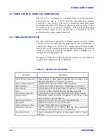
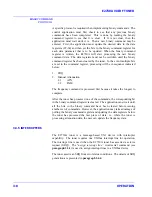
Page 44: ...ble for setting the tuner s tuned frequency The limit of the command is 0 MHz to 2700 MHz The frequency query FRQ is always valid and will return the current tuner frequency The E2730A supports two combinations of tuning speed and tuning resolution These tuning modes are selected by the tuning speed command TSP This allows the tuner tuning to be optimized for either speed or resolution Tuning spee...

Page 45: ...rf Selects tuning resolution 1 100 Hz 2 1 kHz TSP TSP nr1 Request current tuning resolution Reset TSP 2 Example TSP 1 TUNER ATTENUATION OPERATIONS Gain control of the E2730A is via the ATN command The ATN command allows the reduction of gain from maximum ATN 0 in approximately 2 dB increments to gain minimum ATN 56 The commands in this message category are listed in Table 3 7 Table 3 7 Tuner Atten...

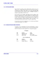
Page 46: ...idual queries DIRECT MEMORY COMMANDS The direct memory commands allow access to memory channels without impacting the current tuner operation The first argument after the SMD or RMD command identifies the channel number which can be zero to indicate current tuner operations or one to 200 to specify a memory channel The remaining fields are the data values associated with the mnemonic parameters as...

Page 47: ...ed 5 COR COR Ignored 6 Detection Mode DET Ignored 7 AGC Mode AGC Ignored 8 Attenuation Setting ATN 0 to 60 9 AFC Mode AFC Ignored 10 Pre Dwell PDW Ignored 11 Signal Dwell SDW Ignored 12 Loss Dwell LDW Ignored 13 Sweep Start Freq FRA Ignored 14 Sweep Stop Freq FRB Ignored 15 Sweep Increment Freq INC Ignored 16 Sweep Direction SWD Ignored 17 BFO Frequency BFO Ignored 18 IFO Frequency IFO Ignored STO...

Page 48: ...ce and the RS 232 interface of the tuner The E2730A supports the IEEE 488 2 SRQ capability This capability is implemented through a series of layered enable and status registers The tuner is capable of generating SRQ interrupts for numerous events These include communication errors and hardware errors The SRQ Structure Diagram is shown in Figure 3 1 This diagram shows the layers of enable and stat...

Page 49: ... event The EXE bit is set to indicate that the tuner has received a valid command with an out of bounds argument The CME bit indicates the tuner has received an unknown or invalid command mnemonic The PON bit is set whenever the unit power is cycled Anytime the control software restarts the PON bit will be set The mnemonics associated with this message category are listed in Table 3 10 Table 3 10 ...

Page 50: ... OPT 000 RTK nrf RTK nr1 Request Token Returned value will either be the number entered or another controller s token value if the token was not zero when the request was received The valid arguments are 0 to 99 Reset n c Power up RTK 00 Example RTK 01 RTK 0 Return token to tuner allowing it to be requested by another controller Sets tuner token to 0 SRE nrf Set up the Service Request Enable Regis...

Page 51: ...E2730A SRQ Structure Diagram 3 4 5 HARDWARE ERROR MESSAGES The E2730A performs both startup built in internal tests and continuous monitoring of key tuner sections The tuner responds to a command which reruns the startup test and also queries to determine the current status of these operations along with the history since the last status request The errors indicated in these messages are all hardw...

Page 52: ...s query returns a latched history of any errors that have occurred since the last read of this register Reading the DDE clears any latched errors If the error condition still exists the bit will be immediately reactivated The TST command responds with same data as the DDE query However the TST status query does not clear the latched device dependent error status register The mnemonics associated w...

Page 53: ...atched error status Reading this register clears it until the fault reoccurs This is a bit mapped response where 0 Okay and 1 Fault Bit Value Description 0 1 Not Used 1 2 Not Used 2 4 Not Used 3 8 Not Used 4 16 FXE FLEX Bootload failure 5 32 1LO 1st LO unlocked 6 64 2LOT 2nd LO Translation Loop unlocked 7 128 2LOR 2nd LO Resolution Loop unlocked 8 256 Not Used 9 512 EED EEPROM has been defaulted 1...

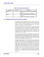
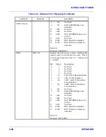
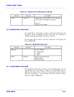
Page 54: ...coherence is required The commands that are used to control the master slave LO operation are listed in Table 3 12 Table 3 12 Master Slave Messages Command Response Description LOM nrf Set the LO Mode 0 Independent 1 Master 2 Slave LOM LOM nr1 Request current LO Mode Reset LOM 0 Example LOM 1 3 4 7 COMPATIBILITY MESSAGES The commands in this message category are only implemented to provide compati...

Page 55: ...E nrf Set ATE Attenuator IGNORED ATE ATE 0 Query value of ATE Attenuator ATF nrf Set Final Attenuator ATF ATF 0 Query value of Final Attenuator ATS nrf Set Second IF Attenuator ATS ATS 0 Request current value of Second IF Attenuator BFO nrf Set BFO frequency BFO BFO 0 00 Request current BFO frequency BUP nrf Sets the sample Bin Update option BUP BUP 0 Request the status of the Bin Update parameter...

Page 56: ...rf nrf Set Video Bandwidth Data IGNORED DBM nrf Set data representation in SSD buffer DBM DBM 0 Request current SSD data representation DBT nrf Set data width number of bits in Digital Scan Output DBT DBT 8 Request Digital Scan Output data width DCM nrf Set DSP Clock Mode DCM DCM 0 Request Current DSP Clock Mode DCR nrf Sets the value of the Delta COR parameter DCR DCR 0 Request the value of the D...

Page 57: ...RB 2700 0000 Request current stop frequency F1 F2 scan GTA nrf Set AGC Gate Timer for AM and FM detection modes GTA GTA 4 Request setting of AGC Gait Timer for AM and FM GTC nrf Set AGC Gate Timer for CW SSB and IFT detection mode GTC GTC 4 Request setting of AGC Gait Timer for CW SSB and IFT detection modes GTP nrf Set AGC Gate Timer for AM Pulse detection mode GTP GTP 4 Request setting of AGC Ga...

Page 58: ...P nrf Sets the number of learning sweep passes LSP LSP 0 Request the number of learning sweep passes MST MST 0 Request Manual operation status OPR nrf Set the tuner operating mode OPR OPR 1 Request current operating mode PDW nrf Set scan pre dwell timer PDW PDW 000 Request current scan pre dwell timer PRE nrf Set Preselector Tuning Voltage PRE PRE 000 Request Current Preselector Tuning Voltage QUE...

Page 59: ...vailable space in lockout memory in unused channels SLP nrf Put radio into Sleep mode SMC Shared Memory Clear SME nrf Set Shared Memory Enable Register SME SME 000 Request current value of Shared Memory Enable Register SMM nrf Shared Memory Data Type SMM SMM 0 Request Shared Memory Data Type SMR SMR 000 Request current value of Shared Memory Status Register SMS nrf nrf Set Shared Memory FIFO Progr...

Page 60: ...o Master radio of a DF set TLM nrf Set the Third LO Mode TLM TLM 0 Request the current Third LO Mode TPE nrf Set trigger pair enable TPE TPE 0 Trigger pair enabled status TPS nrf nrf Selects the two VXI trigger lines for the Shared Memory Trigger and the F Sync Pulse respectively TPS TPS 0 1 Requests the VXI trigger line setting ULC nrf Unlock the channel UPB While stopped or suspended on a signal...

Page 61: ... with this message category are listed in Table 3 14 Table 3 14 User Configuration Messages Command Response Description CBR nrf Set User BAUD Rate for RS 232 port Valid Values 1200 2400 4800 9600 19200 38400 CBR CBR nr1 Request current user BAUD Rate Default CBR 19200 Example CBR 09600 CFG nrf Set configuration status on or off Normal operation is with configuration off 0 When configuration is on...

Page 62: ... parameters the tuner must be removed from the configuration mode by sending CFG 0 The mnemonics associated with this message category are listed in Table 3 15 NOTE Many of these parameters are unique to the particular tuner serial number and should not be changed Table 3 15 Factory Configuration Messages Command Response Description CDT nrf nrf nrf Set the date of configuration Field Parameter Ra...

Page 63: ...number and VXI hexidecimal model code Default MDL E2730A 2B6 Example MDL E2730A 2B6 Note The first six E2730A of the seven characters must never change If they do then the EEPROM will be reset upon the next power up of the unit YCL Initiates a Calibration of the YIG DAC This command should only be issued by qualified personnel and only after the tuner is at normal operational temperature YCL YCL n...

Page 64: ... steps ATI ATI nr1 Request current IF attenuator setting Reset ATI 00 Example ATI 14 ATR nrf Set RF attenuators Range 0 to 30 2 dB steps ATR ATR nr1 Request current RF attenuator setting Reset ATR 00 Example ATR 22 BND nrf Sets the preselector band Range 1 2 Where 1 Selects the lower preselector band 0 982 MHz 2 Selects the upper preselector band 982 MHz BND BND nrl Returns the active preselector ...

Page 65: ...1 nr1 nr1 Read a memory location Field Parameter Range 1 Memory Size 0 byte 1 word 2 long word 2 Memory Address 0 to 4294967295 3 Data Value 0 to 255 0 to 65535 0 to 4294967295 Reset N A Example MEM 0 0000100000 200 PAM nrf Turn Pre Amplifier OFF and ON 0 OFF 1 ON Reset 1 Default 1 PAM PAM nr1 Request Pre Amp Setting ...

Page 66: ...4 i SECTION 4 REPLACEMENT PARTS LIST ...

Page 67: ...4 ii THIS PAGE INTENTIONALLY LEFT BLANK ...

Page 68: ...are used on the equipment and on the manual illustrations This partial reference designation consists of the component type letter s and the identifying component number The complete reference designation may be obtained by placing the proper prefix before the partial reference designation Reference designation prefixes are included on the drawings and illustrations in the figure titles in parenth...

Page 69: ...ay not necessarily be identical with the parts installed in the unit However the parts listed in paragraph 4 5 will provide satisfactory unit operation Replacement parts may be obtained from any manufacturer provided the physical characteristics and electrical parameters of the replacement item are compatible with the original part In the case where components are defined by a military or industri...

Page 70: ...3532 001 14632 A7 Not Used A8 YIG Assembly 1 384286 001 14632 FL1 3 7 GHz Filter Assembly 1 384767 001 14632 J2 Connector Modified 2 384205 001 14632 J8 Same as J2 W1 Cable Assembly 1 17300 530 001 14632 W1J1 Connector Modified 3 384206 001 14632 W1P1 Connector RF Misc Plug Straight Male 4 11MMCX50 2 1C 7W263 MMCX for RG 405 085 S W2 Cable Assembly 1 17300 530 002 14632 W2P1 Connector Plug GPO Rig...

Page 71: ...E2730A VXI RF TUNER 4 4 REPLACEMENT PARTS LIST NOTES ...

Page 72: ...FP i FOLDOUTS ...

Page 73: ...FP ii THIS PAGE INTENTIONALLY LEFT BLANK ...

Page 74: ...FO 1 Type E2730A VXI RF Tuner Main Chassis Schematic Diagram 484331 Sheet 1 of 2 B FP 1 FP 2 blank E2730A VXI RF TUNER ...

Page 75: ...E2730A VXI RF TUNER FO 1 Type E2730A VXI RF Tuner Main Chassis Schematic Diagram 484331 Sheet 2 of 2 B FP 3 FP 4 blank ...

Reviews: