background image

Chapter 2

119

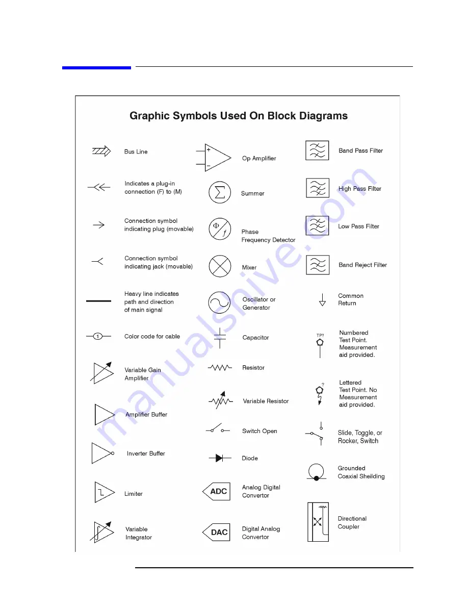
Block Diagrams

Block Diagrams

Block Diagrams

Summary of Contents for E4406A VSA Series

Page 1: ...ervice Guide Agilent Technologies E4406A VSA Series Transmitter Tester Manufacturing Part Number E4406 90178 Supersedes E4406 90125 Printed in USA March 2006 Copyright 1999 2006 Agilent Technologies Inc ...

Page 2: ...te until the indicated conditions are fully understood and met CAUTION Caution denotes a hazard It calls attention to a procedure that if not correctly performed or adhered to could result in damage to or destruction of the instrument Do not proceed beyond a caution sign until the indicated conditions are fully understood and met WARNING This is a Safety Class 1 Product provided with a protective ...

Page 3: ...se with an instrument will execute its programming instructions when properly installed on that instrument Agilent Technologies does not warrant that the operation of the instrument or software or firmware will be uninterrupted or error free LIMITATION OF WARRANTY The foregoing warranty shall not apply to defects resulting from improper or inadequate maintenance by Buyer Buyer supplied software or...

Page 4: ...4 ...

Page 5: ...RF Analog IF Digital IF Reference Synthesizer or CPU Problem 39 Verifying the A17 RF Assembly 39 Verifying the A12 Analog IF Assembly 43 Verifying the A10 Digital IF Assembly 47 Verifying the A18 Reference Assembly 50 Verifying the A19 Synthesizer Assembly 52 Verifying the A22 CPU Assembly 54 Troubleshooting Performance Test Failures 58 Contacting Agilent Technologies 60 Software Technical Support...

Page 6: ...nput Selector Switch 76 Offset Adjust and Dither 77 Interconnections to other assemblies 77 A18 Reference Assembly 78 100 MHz VCXO 78 300 MHz Output 79 Reference Unlock Detector 79 50 MHz Calibrator Output 79 10 MHz Outputs 79 Interconnections to other assemblies 79 A19 Synthesizer Assembly 80 Lock Detector 80 VCO Phase Lock Loop 80 Bandpass Filters 80 First Doubler 80 Second Doubler 81 Interconne...

Page 7: ...ter an instrument repair 167 Removal and Replacement Procedures 168 Instrument Outer Case 171 Removal 171 Replacement 172 Top Brace 173 Removal 173 Replacement 174 Front Frame 175 Drop the Front Frame 175 Removal 175 Replacement 176 A4 Disk Drive and A5 Disk Drive Board 177 Removal 177 Replacement 179 A6 Power Supply 180 Removal 180 Replacement 181 A7 Baseband I Q Assembly Option B7C 182 Removal 1...

Page 8: ...8 Replacement 209 Rear Frame 210 Removal 210 Replacement 211 Center Web Cables W9 W11 and W12 212 Removal and Replacement 212 RF Input Connector 214 Removal 214 Replacement 215 Front Frame Subassemblies 216 Front Frame Exploded View 218 A2 Display Backlights and Filter 219 A3 Front Panel Interface Board 224 Bezel and Keypad 226 Front Panel RPG 229 Front Panel External Trigger Cable 230 5 Post Repa...

Page 9: ...uency Reference Adjustment 248 Adjustment Description 248 Required Equipment 248 Test Setup 249 Procedure 249 Internal 50 MHz Calibrator Adjustment 250 Description 250 Required Equipment 250 Test Setup 251 Procedure 251 Burst Trigger Check 254 Description 254 Procedure 254 Baseband I Q Amplitude Accuracy Test 255 Description 255 Test Limits 255 Procedure 255 Using the Alpha Editor Menu 258 Front P...

Page 10: ...10 Contents ...

Page 11: ...11 1 Troubleshooting ...

Page 12: ...roubleshooting Introduction Introduction This chapter provides information and procedures that are useful for troubleshooting common instrument failures Assembly descriptions are located in Chapter 2 Block Diagrams ...

Page 13: ...his section WARNING These servicing instructions are for use by qualified personnel only To avoid electrical shock do not perform any servicing unless you are qualified to do so WARNING The opening of covers or removal of parts is likely to expose dangerous voltages Disconnect the product from all voltage sources while it is being opened WARNING The detachable power cord is the instrument disconne...

Page 14: ...bly A18 reference assembly A19 synthesizer assembly A21 motherboard A22 CPU processor assembly does not include A22A1 A2 or A3 A22A1 DRAM card A22A2 Flash memory board A22A3 GP IB capacitor board A25 SCSI board A27 rear panel connector board A3A1 A3A2 inverter board After an Instrument Repair If an instrument assembly has been repaired or replaced perform the related adjustments and performance ve...

Page 15: ...rist strap combination Conductive floor mat and heel strap combination Both types when used together provide a significant level of ESD protection Of the two only the table mat and wrist strap combination provides adequate ESD protection when used alone To ensure user safety the static safe accessories must provide at least 1 M Ω of isolation from ground Refer to Table 1 1 for information on order...

Page 16: ...udes 3M static control mat 0 6 m 1 2 m 2 ft 4 ft and 4 6 cm 15 ft ground wire The wrist strap and wrist strap cord are not included They must be ordered separately 9300 0980 Wrist strap cord 1 5 m 5 ft 9300 1383 Wrist strap color black stainless steel without cord has four adjustable links and a 7 mm post type connection 9300 1308 ESD heel strap reusable 6 to 12 months ...

Page 17: ... damage to components and prevent contamination of exposed plating Test Equipment Usage and ESD Before connecting any coaxial cable to an instrument connector for the first time each day momentarily short the center and outer conductors of the cable together Personnel should be grounded with a 1 M Ω resistor isolated wrist strap before touching the center pin of any connector and before removing a...

Page 18: ...z Spectral purity 1 MHz to 1321 MHz SSB Phase Noise at 1 GHz 106 dBc Hz at 1 kHz offset or residual FM 0 5 Hz 300 Hz to 3 kHz integration BW Spurious non harmonic 78 dBc SWR 1 5 8663A A P T Synthesized Signal Generator Frequency 960 MHz Spectral purity SSB Phase Noise 150 dBc Hz at 100 kHz offset Harmonics 30 dBc at 10 dBm output 8665A B P Synthesized Swept Signal Generator Frequency 10 MHz to 4 0...

Page 19: ...z SWR 50 MHz 1 10 1 MHz to 4 GHz 1 30 8482A P Power Sensor High sensitivity Used to measure 25 dBm signal at 50 MHz only requires a 30 dB pad 8481D A Oscilloscope Digitizing Oscilloscope 150 MHz 54602B 54820A T Standards Frequency Standard Frequency 10 MHz Accuracy 1 X10 10 5071A A P Attenuators 10 dB Step Attenuator Range 0 to 110 dB Accuracy Characterized by standards lab to 0 005 0 0052 10 dB s...

Page 20: ...litter Frequency 1 MHz to 4 0 GHz SWR 1 1 11667A 11667B P Directional Bridge Frequency Range 0 1 to 110 MHz Directivity 40 dB VSWR 1 1 Transmission Arm Loss 6 dB nominal Coupling Arm Loss 6 dB nominal 8721A P High Frequency Probe 300 kHz to 3 GHz Input Resistance 1 MΩ nominal 85024A T Attenuator Interconnector Kit Type N For 8496G and 8494G attenuators 11716A P Cables Type N 2 required Precision T...

Page 21: ...rface Card High performance GP IB or GPIBc Must support VTL 82341D 82350B 82357A National p n AT GPIB TNT P A Software Performance verification and adjustment software for E4406 VSA N7812A P A Service Kit Includes three extender boards required for troubleshooting E4406 60114 T Hand Tools Torx Driver T 10 8710 1623 Torx Driver T 15 8710 1622 Torx Driver T 20 8710 1615 Nut Driver 9 16 inch deep soc...

Page 22: ...22 Chapter1 Troubleshooting Service Equipment You Will Need c National Instruments GPIB card or GP IB card with VISA I O library installed available at http www natinst com gpib gpib_dl htm ...

Page 23: ...tions and capabilities of the instrument Refer to the specifications book for instrument specifications 7 In order to meet specifications the instrument must be aligned Press System Alignments Align All Now The diagnostic tests should all pass If the instrument displays a failure during these tests refer to Auto Align Tests on page 32 8 Check to see if the instrument has the latest firmware before...

Page 24: ...n page 26 Instrument did not boot Check for Basic Functionality on page 31 Power on auto align tests failed Auto Align Tests on page 32 No response when a key is pressed Check for Basic Functionality on page 31 Error messages See the Agilent Technologies E4406A VSA Instrument Messages and Functional Tests manual Low signal level Isolating an RF Analog IF Digital IF Reference Synthesizer or CPU Pro...

Page 25: ...wered up These tests evaluate the instrument operation and will return an error message if a problem is detected 1 If the instrument appears to be dead no display or the fans are not operating refer to Troubleshooting an Inoperative Instrument on page 26 2 If the instrument appears to abort the boot process or there is no response when a front panel key is pressed refer to Check for Basic Function...

Page 26: ...tial checks when first troubleshooting an inoperative instrument 1 Check the instrument display and fans a If the display is dark and the fans are not running suspect a power supply or CPU problem Refer to the Power Supply Check on page 34 b If the display is dark but the fans are running suspect either an LCD problem or a problem with the CPU boot sequence Refer to Troubleshooting LCD Display Pro...

Page 27: ...4 fan control board Refer to Chapter 3 for assembly replacement procedures If only one or two fans are not functioning and the power supplies are within specifications suspect the A14 fan control board or a defective fan 1 Remove the front frame from the instrument Refer to Chapter 3 for removal procedures 2 Refer to Figure 1 2 Measure all of the fan voltages at J1 J3 and J4 on the motherboard Fig...

Page 28: ...ly plugged into the motherboard at connector J11 4 If W8 is properly connected suspect a defective A3 front panel interface board one or both of the inverter boards A3A1 and A3A2 mounted on the interface board the backlight assemblies DS1 and DS2 or the LCD assembly itself A2 5 If the display is dim suspect the backlight assemblies Always replace both backlight bulbs at the same time Verifying the...

Page 29: ... 5 input 33 4 mV CN1 pin 3 26 mV T1 pin 6 input 30 Vdc CN1 pin 4 33 mV T1 pin 7 output 60 V p p sinewave 38 kHz CN1 pin 5 33 mV T1 pin 9 output 77 V p p sinewave 38 kHz CN1 pin 6 33 mV T1 pin 10 output 450 V p p sinewave 38 kHz T1 pin 1 input 30 Vdc T1 pin 12 output 45 V p p sinewave 38 kHz T1 pin 2 input 3 3 Vdc CN2 A 400 V to 400 V sinewave 38 kHz see figure T1 pin 3 input 3 3 Vdc CN2 B 2 15 V t...

Page 30: ...s as indicated in Figure 1 4 If all of these signals measure correctly suspect a defective backlight or LCD The backlight is the most probable cause NOTE The P2 connector on the front panel interface board has supports soldered at each end as shown in the figure Make sure to measure the correct pins Be very careful when measuring these signals to ensure you do not short out any pins Figure 1 4 Ver...

Page 31: ...elf diagnostic tests when powered up These tests evaluate the instrument operation and will return an error message if a problem is detected If the instrument does not boot check that the CPU is functioning Refer to Verifying the A22 CPU Assembly on page 54 If the instrument boots and there are auto alignment error messages refer to Auto Align Tests on page 32 to help isolate the problem ...

Page 32: ...bit control dac on the A12 analog IF If it is not monotonic or the expected variation is not verified this alignment will FAIL ADC Offset DACs Offset dacs for each of the 6 ADC range positions on the A10 digital IF assembly are aligned to reduce the overall DC offset ADC Dither CF The ADC dither needs to be centered to prevent its own harmonics from folding back into the center of the IF passband ...

Page 33: ...ain setup during a measurement XTAL Prefilter Narrow See description for XTAL Prefilter Wide ADC Autorange The ADC autoranging subsystem has several hardware components that need to be setup This alignment takes care of 3 dacs 2 dacs on the A10 digital IF assembly that set the positive and negative thresholds for range switches and 1 dac on the A12 analog IF assembly that sets the GAIN of the auto...

Page 34: ... lit green LED indicates the power supply has received an ON command and that the 5 2 VDC supply can at least light the LED 3 The front panel probe power connector can be used to check the 15 VDC and 12 5 VDC 15 VDC supplies The 12 5 VDC is produced by post regulating the 15 VDC supply Refer to Figure 1 5 for a diagram of the probe power connector Figure 1 5 Probe Power Connector If all of these s...

Page 35: ...ltages Refer to the safety symbols provided on the instrument and in the general safety instructions in this guide before operating the unit with the cover removed Ensure that safety instructions are strictly followed Failure to do so can result in severe or fatal injury The power supply voltages are checked using a digital voltmeter Voltages measured should be within the tolerances listed in the ...

Page 36: ...0021 Extender Measurement Locations Measurement Location Signal Description Test Equipment Used Expected Level A power supply DVM 5 2 VDC B power supply DVM 5 2 VDC C power supply DVM 15 VDC D power supply DVM 15 VDC E power supply DVM 9 VDC F power supply DVM 32 VDC ...

Page 37: ...he supply is now up suspect the last assembly removed as being defective Remove these assemblies first refer to Chapter 3 for removal instructions A17 RF assembly A18 reference assembly A19 synthesizer assembly A12 analog IF assembly A10 digital IF assembly A7 base band IQ assembly Option B7C Other assemblies to remove include A25 SCSI A3 front panel interface assembly A15 daughterboard assembly A...

Page 38: ...ng boards from the instrument in the following order and recheck the shorted test point after each board is pulled Note that the resistance will be different from the table but you should be able to tell if the shorted condition has changed First pull the A14 fan control board followed by the A22 CPU assembly and finally the A6 power supply If All Voltage Supplies Are Good If all of the supplies h...

Page 39: ...bly The A17 RF assembly uses two internal mixers to down convert the instrument s input signal to the 2nd IF of 21 4 MHz You can verify the performance of the RF assembly by injecting a 50 MHz CW signal at the front panel RF input connector and measuring the 21 4 MHz output signal level The default attenuator setting is 0 dB Refer to Figure 1 7 for two examples of the down conversion process one w...

Page 40: ...l cable Measure the 21 4 MHz 2nd IF output from the A17 RF assembly going to the A12 analog IF assembly 6 If the A17 RF assembly is operating properly the 21 4 MHz 2nd IF out of the A17 RF assembly will measure 25 dBm on the calibrated spectrum analyzer NOTE Note that this power level was obtained using a 50Ω BNC to SMB cable If a high frequency probe such as the 85024A is used the power level wil...

Page 41: ...ld read 25 dBm on the instrument display If this power level is correct and the RF input signal from the external 50 MHz source is displayed at the wrong amplitude the AT1 7 dB pad the RF input connector or the input switch on the A17 RF assembly may be defective The remaining detailed checks require the A17 RF assembly to be placed on an extender board p n E4406 60042 Turn the instrument off befo...

Page 42: ...supply DVM 15 VDC D power supply DVM 6 VDC E power supply DVM 9 VDC F power supply DVM 32 VDC G power supply DVM 5 2 VDC H 300 MHz 2nd L O In calibrated spectrum analyzer 8 75 dBm I 50 MHz Internal Calibrator calibrated spectrum analyzer 18 4 dBm J 321 4 MHz 1st IF Out calibrated spectrum analyzer 29 dBm K RF Input calibrated spectrum analyzer 32 dBm L a a Remember to measure on the LO board side ...

Page 43: ...ectrum analyzer to the end of this flexible cable and measure the 7 5 MHz output from the A12 analog IF assembly going to the A10 digital IF assembly 6 If the A12 analog IF assembly is operating properly the 7 5 MHz 3rd IF out of the A12 assembly will measure 22 5 dBm on the calibrated spectrum analyzer 7 Reconnect the cable to A10P7 Analog IF Assembly Detailed Troubleshooting If the quick check p...

Page 44: ... Wide mode or the 12 5 MHz Low Pass Post Filter and the A12 analog IF assembly is defective 8 Change the span on the instrument by pressing Span 30 kHz 9 Press Meas Setup More Advanced Pre FFT Fltr Check that Gaussian is still underlined 10 Press Pre FFT BW and enter 50 kHz If the signal level on screen is 25 dBm the failure mode is in the LC Narrow mode and the A12 analog IF assembly is defective...

Page 45: ... refer to Figure 1 9 for the measurement locations Verify the voltages in the table below the figure If the levels in the table are correct and bypassing the pre and post filters does NOT improve the power level the most probable cause is the A12 analog IF assembly Pre FFT BW Setting Pre filter Being Used Actual Pre filter BW Gaussian Fltr Mode Pre filter BW Range Post filter Being Used 2 kHz XTAL...

Page 46: ...ment Locations Measurement Location Signal Description Test Equipment Used Expected Level A power supply DVM 5 2 VDC B power supply DVM 5 2 VDC C power supply DVM 15 VDC D power supply DVM 15 VDC E power supply DVM 9 VDC F power supply DVM 32 VDC G Gate Arm DVM 3 7 VDC H Gate Trig DVM 3 7 VDC I Sweep Arm DVM 3 7 VDC J Sweep Trig DVM 3 7 VDC ...

Page 47: ...gnal at 50 MHz at 25 dBm into the RF input of the instrument 2 Press Preset on the instrument and tune to 50 MHz by pressing Input Input Port RF Frequency 50 MHz 3 Press Input and verify the input attenuation is set to 0 dB by viewing the 5th softkey from the top If it is not at 0 dB press Input Atten and enter 0 dB 4 Connect a calibrated spectrum analyzer to A10TP5 5 The 7 5 MHz 3rd IF power leve...

Page 48: ... Problem Figure 1 10 E4406 60021 Extender Measurement Locations Measurement Location Signal Description Test Equipment Used Expected Level A power supply DVM 5 2 VDC B power supply DVM 5 2 VDC C power supply DVM 15 VDC D power supply DVM 15 VDC E power supply DVM 9 VDC F power supply DVM 32 VDC ...

Page 49: ...m NOTE To access the G through J measurement points in Figure 1 11 it is necessary to remove the small shield on the A10 digital IF assembly Figure 1 11 A10 Clock Measurements for the E4440 60025 E4440 60195 Digital IF Assembly Figure 1 12 A10 Clock Measurements for the E4406 60006 Digital IF Assembly ...

Page 50: ... from this assembly as well by dividing the 100 MHz VCXO by 2 Verify the 10 MHz references by extending the A18 reference assembly Reference Assembly Quick Check Turn the instrument off before removing a PC board assembly from the instrument The remaining quick checks require the A18 reference assembly to be placed on an extender board p n E4406 60042 The A17 RF assembly must also be removed to be...

Page 51: ...er supply DVM 5 2 VDC H 300 MHz 2nd L O calibrated spectrum analyzer 5 5 dBm I 50 MHz Int Cal a a The internal calibrator must be switched in to obtain an accurate level for the 50 MHz Int Cal measurement Press Input Input Port 50 MHz Ref calibrated spectrum analyzer 13 dBm M 10 MHz Synth From Ref calibrated spectrum analyzer 17 5 dBm N 10 MHz Opt calibrated spectrum analyzer 13 dBm P 10 MHz RF fr...

Page 52: ... example if the center frequency of the instrument is set to 3678 5 MHz the 1st L O is 3678 5 MHz 321 4 MHz 3999 9 MHz almost max As soon as the instrument is set to a center frequency of 3678 6 MHz and greater the 1st L O will shift to 3678 6 MHz 321 4 MHz 3357 2 MHz The best location to measure the 1st L O frequency and power level is when the A17 RF assembly is placed on an extender board p n E...

Page 53: ...tions Measurement Location Signal Description Test Equipment Used Expected Level A power supply DVM 15 VDC B power supply DVM 5 2 VDC C power supply DVM 15 VDC D power supply DVM 6 VDC E power supply DVM 9 VDC F power supply DVM 32 VDC G power supply DVM 5 2 VDC T 10 MHz Synth to Synth calibrated spectrum analyzer 17 5 dBm U Pre Level Drive DVM 2 5 VDC ...

Page 54: ...t firmware the synthesizer cal values plus any options and keywords loaded into the instrument CPU Assembly Quick Check Following power up the instrument will perform a boot process as follows Once power is applied to the instrument the screen will remain blank for several seconds Text begins to scroll by on the instrument display as the instrument boots from the bootrom During this time you will ...

Page 55: ...Ds will flash on and off as the instrument steps through the boot up sequence At the end of the sequence all of the green LEDs should be off If one or more of the green LEDs remains on suspect the processor assembly as being defective If a LAN cable is attached it is normal for the yellow LEDs to flash indicating LAN activity If a LAN cable is attached the link integrity LED will also light up Fig...

Page 56: ...ware files on the A22A2 Flash board may be defective Try loading new firmware before replacing the A22 processor or A22A2 Flash assemblies Look at the instrument screen and read any error messages that might appear The messages can give you a clue as to what is happening when the instrument hangs up Battery If you are experiencing problems with the real time clock in your instrument it might be ti...

Page 57: ...lies on A21J17 Pins 1 and 2 should measure 12 VDC Pins 3 and 4 should measure 12 VDC If the power supplies measure correctly and the CPU does not boot properly the I O lines could be loaded down by another assembly or a clock signal could be missing Remove the A10 digital IF assembly and try rebooting The A12 analog IF assembly must be installed and providing the 30 MHz sample clock before the CPU...

Page 58: ...ng Performance Test Adjustment Probable Faulty Assembly Next Step Displayed Average Noise Level DANL None A17 RF A12 analog IF A10 digital IF Step 5 Attenuator Accuracy at 50 MHz None A17 RF Amplitude Linearity None A10 digital IF A12 analog IF Step 3 Absolute Amplitude Accuracy Frequency Response Flatness Internal 50 MHz Calibratora A12 analog IF A17 RF A10 digital IF Step 4 Third Order Intermodu...

Page 59: ...g the failure Use this information to help isolated the failure Go to Isolating an RF Analog IF Digital IF Reference Synthesizer or CPU Problem on page 39 Step 5 Use a spectrum analyzer to trace a signal through the RF input path to determine where the extra noise is being added See the E4406A Overall Block Diagram in Chapter 2 Go to Isolating an RF Analog IF Digital IF Reference Synthesizer or CP...

Page 60: ...nt N7812A Calibration Application Software contact Agilent Technologies for assistance For software technical support contact the Agilent Technologies Test and Measurement Call Center at 1 800 452 4844 Calling Agilent Technologies Sales and Service Offices Use the information in this section to obtain Agilent Technologies sales and service offices information Sales and service offices are located ...

Page 61: ...4 495 8950 Japan tel 81 426 56 7832 fax 81 426 56 7840 Australia tel 1 800 629 485 fax 61 3 9210 5947 Asia Call Center Numbers Country Phone Number Fax Number Singapore 1 800 375 8100 65 836 0252 Malaysia 1 800 828 848 1 800 801664 Philippines 632 8426802 1 800 16510170 PLDT Subscriber Only 632 8426809 1 800 16510288 PLDT Subscriber Only Thailand 088 226 008 outside Bangkok 662 661 3999 within Ban...

Page 62: ...first provides the identification number for each option built into the instrument and the second provides the instrument s serial number The serial number has two parts the prefix two letters and the first four numbers and the suffix the last four numbers Refer to Figure 1 17 Figure 1 17 Example Serial Number The first two letters of the prefix identify the country in which the unit was manufactu...

Page 63: ...bleshooting Updating Firmware Updating Firmware Please refer to http www agilent com vsa for the latest E4406A firmware and installation instructions Firmware updates are performed via a LAN hub or LAN cross over cable ...

Page 64: ...ual Please be as specific as possible about the nature of the problem If you have recorded any error messages that appeared on the screen or have completed a Performance Test Record or have any other specific data on the performance of the instrument please send a copy of this information with the unit Original Packaging Before shipping pack the unit in the original factory packaging materials if ...

Page 65: ...discharge 4 Use a strong shipping container A double walled corrugated cardboard carton with 159 kg 350 lb bursting strength is adequate The carton must be both large enough and strong enough to accommodate the instrument Allow at least 3 to 4 inches on all sides of the instrument for packing material 5 Surround the equipment with three to four inches of packing material and prevent the equipment ...

Page 66: ...66 Chapter1 Troubleshooting How to Return Your Instrument for Service ...

Page 67: ...67 2 Block Diagrams ...

Page 68: ...ctor spectrum analysis and time gated spectrum analysis Simultaneous time and frequency domain measurements and displays improve productivity and enhance ease of use This chapter briefly describes each of the following instrument assemblies A6 Power Supply Assembly on page 69 A10 Digital IF Assembly on page 76 A12 Analog IF Assembly on page 73 A17 RF Assembly on page 70 A18 Reference Assembly on p...

Page 69: ...s the input power and switches between these two ranges The output voltages are 5 2 V 5 2 V 9 V 15 V 15 V 32 V VCC 5 2 V for processor and VDL 3 3 V to processor A low TTL level on the PS_off_L line turns off the power supply and places it in standby mode In standby mode the front panel standby LED is powered on by the P15SBY line from the power supply When the power supply is on the power on fron...

Page 70: ...Hz second LO and being down converted to 21 4 MHz The cal switch allows a 321 4 MHz cal signal to be switched into the signal path when the instrument performs auto cal The 321 4 MHz cal signal is produced by mixing the 300 MHz second LO signal with a 21 4 MHz modulated Cal_Osc signal The Cal_Osc signal is produced on the A12 analog IF assembly and can be a pulse a comb or a cw signal The RF assem...

Page 71: ...zer assembly For input signals less than or equal to 3678 6 MHz the LO frequency is calculated as the RF 321 4 MHz For signals above 3678 6 MHz the LO frequency is calculated as the RF 321 4 MHz 321 4 MHz Amplifiers The amplifiers in the 321 4 MHz IF path are low noise high dynamic range Calibrator Switch A 321 4 MHz calibrator signal is generated on the A17 RF assembly The cal switch selects betw...

Page 72: ...idth of approximately 12 MHz Pre level Drive The pre level drive is part of the AGC loop After detecting the level of the LO on the RF board the pre level drive drives a variable attenuator on the A19 synthesizer board which then adjusts the level of the LO Interconnections to other assemblies A17P1 21 4 MHz out to the A12 analog IF board A17P2 RF input 7 MHz to 4 GHz from the front panel port A17...

Page 73: ...level to the mixer provides a 21 4 MHz anti alias filter provides the final down conversion performs post down conversion filtering provides calibrator oscillator and sample rate oscillator provides a clock generator performs the third LO conversion triggering provides the power supply switching frequency generator Pre filters LC and XTAL prefilters are used to attenuate the out of band signals th...

Page 74: ...final IF The 12 5 MHz low pass filter removes high order mixing products from the third LO as well as the 21 4 MHz feed through The 2 MHz wide band pass filter provides additional filtering for narrow resolution bandwidths and is used to improve dynamic range free of spurious signals Calibrator and Sample Rate Oscillators A host of complex signals are used during the vector calibration This output...

Page 75: ...The power supply switches at a rate of 244 kHz This frequency rate is determined by the power supply switching circuitry on the A12 analog IF assembly Interconnections to other assemblies A12J13 21 4 MHz at 2 dBm in from the A17 RF board A12J5 Front panel external trigger input A12J18 Rear panel external trigger input A12P2 7 5 MHz at 5 dBm out to A10 digital IF assembly ...

Page 76: ...will clip the ADC causing erroneous measurement results Gain Range Select Rules This input path is a tapped 21 4 MHz second IF from the A12 analog IF assembly which bypasses the 10 MHz anti alias filters The gain range for the A10 assembly with the variable amplifier before the ADC is 0 to 18 dB Note For instruments that have an A10 assembly with part number E4406 60006 the gain range is 6 dB to 2...

Page 77: ...quirements for the complex ADC chip to function properly The dither generator adds noise to the ADC which converts distortion errors into excess noise It is desirable to diminish distortion at the cost of noise Interconnections to other assemblies A10P7 7 5 MHz at 5 dBm in from A12 Analog IF board ...

Page 78: ...mbly utilizes a phase lock loop which provides stabilization for all the internal reference oscillators used throughout the instrument The reference assembly performs the following function phase locks the 100 MHz VCXO to an internal 10 MHz frequency reference or to an externally provided standard ranging from 1 MHz to 30 MHz provides a phase locked 300 MHz 100 MHz 3 second LO to the A17 RF assemb...

Page 79: ...sembly 50 MHz Calibrator Output The 50 MHz 100 MHz x 2 internal calibrator is used to perform background calibration on various assemblies in the instrument This signal is routed to the A17 RF assembly where it is level shifted Š 10 MHz Outputs The 100 MHz VCXO which is phase locked to a frequency reference is divided by ten resulting in a 10 MHz signal This signal is used on various assemblies in...

Page 80: ...preted by the A22 CPU and display an LO unlock error message in the error message block on the instrument display VCO Phase Lock Loop The VCO range is 500 MHz to 1000 MHz The frequency output of the VCO depends on the center frequency of the instrument This output frequency is very stable because it is phase locked to the 10 MHz reference signal from the A18 reference assembly Bandpass Filters The...

Page 81: ...ubler The center frequency of the instrument will determine the signal path through the second doubler The fundamental VCO frequency may bypass this block of circuitry Interconnections to other assemblies A19J6 LO out 250 MHz to 4 GHz at 10 dBm to the A17 RF board ...

Page 82: ...O connections on the rear panel of the instrument Many of these connectors are soldered directly into the CPU board or plug into the CPU These connections include the following SCSI 2 connector Used for connecting an external CD ROM drive that can be used to update the operating system Parallel interface connector Used to connect the instrument to a parallel printer LAN connector Used for download...

Page 83: ...nd 1 MΩ can be selected through the front panel The 50Ω and1 MΩ can be used for unbalanced inputs while the 600Ω and 1 MΩ impedance setting can be used for balanced inputs Protection is provided against excessive ESD transient and DC input voltages using varister clamps Input Amplifiers The first of three input amplifiers allows for high impedance positive and negative inputs signals while the sec...

Page 84: ...d A18 Frequency Reference Assembly boards The 10 MHz reference signal comes from the A18 board If the 1 to 30 MHz external reference is selected the A15 daughterboard will output the external reference signal to the A18 board Triggering signals for external equipment are input into the A15 daughter board A21 Motherboard The A21 motherboard provides the following functions 1 Provides a load to the ...

Page 85: ... the A22 CPU assembly Any SCSI drive can be used with this SCSI board The SCSI board will mainly be used for connecting an external CD ROM drive The SCSI board assembly also provides a connector for an external keyboard This keyboard connector is compatible with an external AT style PC keyboard ...

Page 86: ... inverter boards provide a stepped up voltage to both backlights on the LCD display A4 Disk Drive The disk drive is used to download information from a 3 5 inch floppy disk to instrument memory and to load information from the instrument onto a floppy disk A27 Rear Panel Four connectors are located on the rear panel of the instrument External Reference The external reference allows you to select a...

Page 87: ...om the reference board to the RF board 300MHZ 300 MHz reference from the reference board to the RF board ABUS Analog bus output from the synthesizer board to test point on the daughterboard ACOM Analog ground chassis AUDIO Line level audio output from the 4 option board slots on the motherboard to the CPU board CALOSC_H Differential ECL 21 4 MHz calibration oscillator output from the analog IF boa...

Page 88: ...t panel display blue 1 signal from the CPU board to the front panel interface board FP_BLUE2 Flat panel display blue 2 signal from the CPU board to the front panel interface board FP_BLUE3 Flat panel display blue 3 MSB signal from the CPU board to the front panel interface board FP_CBLANKL Flat panel display blanking signal from the CPU board to the front panel interface board FP_CLK Front panel b...

Page 89: ...e CPU board to the front panel interface board FP_RED3 Flat panel display red 3 MSB signal from the CPU board to the front panel interface board FP_VSYNCL Flat panel display vertical sync signal from the CPU board to the front panel interface board FP_W_RL Front panel bus read write signal from the CPU board to the front panel interface board GATE_ARM Gate arm signal from the analog IF board to th...

Page 90: ...log IF board P12 12 V power supply from the motherboard to the CPU board P15 15 V power supply on the motherboard P15SBY 15 V standby power supply on the motherboard P32 32 V power supply on the motherboard P5 2 5 2 V power supply on the motherboard ID0 Motherboard option board slot ID bit 0 ID1 Motherboard option board slot ID bit 1 P9 9 V power supply on the motherboard PCMCIA_AD0 not used PCMCI...

Page 91: ...al IF board to the all vertical boards SR_H Differential ECL sample rate clock from the analog IF board to the digital IF board SR_L Differential ECL sample rate clock from the analog IF board to the digital IF board SWEEP_ARM Sweep arm signal from the analog IF board to the digital IF board SWEEP_TRIG Sweep trigger signal from the analog IF board to the digital IF board SW_IN_L Power switch signa...

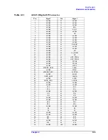
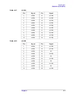
Page 92: ...cated on other pins on this connector Refer to the pinout tables of the individual connectors later in this chapter for a complete listing Table 2 2 A21 Motherboard Mnemonic Locations Mnemonic A21 Motherboard Connector J2 J5 J6 J7 J8 J13 J14 J15 J9 J10 J11 J12 J16 J17 AUDIO_ SPKR NC 92 AUDIO_ SPKR NC 93 10MHZ_AIF 46 57 10MHZ_CPU 50 51 10MHZ_OPT 48 52 ACOM 4 2 1 1 1 1 35 1 1 49 AUDIO 62 AUDIO LINE_...

Page 93: ... FP_A2 54 55 FP_A3 55 56 FP_BLUE0 80 81 FP_BLUE1 81 82 FP_BLUE2 82 83 FP_BLUE3 83 84 FP_CBLANKL 69 70 FP_CLK 65 66 FP_CSL 67 68 FP_D0 56 57 FP_D1 57 58 FP_D2 58 59 FP_D3 59 60 FP_D4 60 61 FP_D5 61 62 FP_D6 62 63 FP_D7 63 64 FP_DOTCLK 68 69 FP_GREEN0 76 77 FP_GREEN1 77 78 FP_GREEN2 78 79 Table 2 2 A21 Motherboard Mnemonic Locations Mnemonic A21 Motherboard Connector J2 J5 J6 J7 J8 J13 J14 J15 J9 J1...

Page 94: ... FP_RED0 72 73 FP_RED1 73 74 FP_RED2 74 75 FP_RED3 75 76 FP_VSYNCL 71 72 FP_W_RL 64 65 GATE_ARM 27 27 GATE_TRIG 29 29 GPIB_TRIG 65 87 HPUP 35 72 72 72 LADDR 28 79 79 79 LCNTRL 32 75 75 75 LDATA 30 77 77 77 LINE_OUT_COM 98 45 LINE_OUT_L 99 94 LINE_OUT_R 97 95 LINE_TRIG 40 67 LO_LOCK 41 66 LSRQ 34 73 73 73 Table 2 2 A21 Motherboard Mnemonic Locations Mnemonic A21 Motherboard Connector J2 J5 J6 J7 J8...

Page 95: ...3 4 43 44 8 46 47 96 97 46 47 96 97 46 47 96 97 P15SBY 40 80 2 3 52 53 P32 1 41 5 6 55 56 49 99 49 99 49 99 P5 2 38 15 24 32 33 82 83 32 33 82 83 32 33 82 83 P5 2 ID0 27 P5 2 ID1 29 P9 6 7 46 47 12 42 43 92 93 42 43 92 93 42 43 92 93 PCMCIA_AD0 68 PCMCIA_AD1 69 PCMCIA_AD2 70 PCMCIA_CLK7 62 PCMCIA_CS1L 63 PCMCIA_CS2L 64 PCMCIA_D0 71 PCMCIA_D1 72 PCMCIA_D2 73 PCMCIA_D3 74 Table 2 2 A21 Motherboard M...

Page 96: ...9 90 PROBE_P15 13 85 86 87 PS_FREQ 39 52 PS_OFF_L 30 79 RANGE 62 62 REMOTE_ON_L 32 86 SCLK 29 78 78 78 SR_H 55 55 SR_L 54 54 SWEEP_ARM 23 23 SWEEP_TRIG 25 25 SW_IN_L 29 TRIG1 36 71 71 71 TRIG2 37 70 70 70 VCC 21 22 24 26 19 21 3 55 VDL 28 3 7 11 15 13 15 17 19 56 VFAN 21 22 23 VFAN 1 2 3 Table 2 2 A21 Motherboard Mnemonic Locations Mnemonic A21 Motherboard Connector J2 J5 J6 J7 J8 J13 J14 J15 J9 J...

Page 97: ...Z_EXT_IN 13 10MHZ_EXT_OUT 2 10MHZ_OPT 17 10MHZ_RF 16 6 10MHZ_SYNTH 8 15 50MHZ 13 300MHZ 18 ABUS 9 ACOM 1 1 1 1 1 1 1 1 1 1 1 CALOSC_H 18 CALOSC_L 19 CLEAN_CK 24 CLEAN_DATA 11 CLEAN_EN 25 MIDGEN_CLEAN 10 N15 2 17 2 17 2 17 2 17 N5 2 4 19 4 19 4 19 4 19 N6 3 18 3 18 3 18 3 18 P15 6 21 6 21 6 21 6 21 P15SBY 22 J32 P32 7 7 7 7 P5 2 14 29 14 29 14 29 14 29 P9 5 20 5 20 5 20 5 20 PRE_LEVEL_ DRIVE 2 17 R...

Page 98: ...nnectors REF_EN 25 J32 RF_CK 24 J22 RF_DATA 11 J22 RF_EN 25 J22 SYNTH_CK 24 SYNTH_DATA 11 SYNTH_EN 25 Table 2 3 A15 Daughterboard Mnemonic Locations Mnemonic A15 Daughterboard Connector J11 J41 J12 J13 J21 J22 J32 J23 J33 J31 J42 J43 J51 J53 J52 ...

Page 99: ...ector Pin Signal Pin Signal 1 VFAN 21 VFAN 2 VFAN 22 VFAN 3 VFAN 23 VFAN 4 ACOM 24 P15 5 ACOM 25 P15 6 ACOM 26 P15 7 ACOM 27 NC 8 ACOM 28 DAUGHTER_OTP 9 ACOM 29 SW_IN_L 10 ACOM 30 PS_OFF_L 11 ACOM 31 POWFAILL 12 ACOM 32 REMOTE_ON_L 13 PROBE_P15 33 ACOM 14 ACOM 34 P15 15 PROBE_N12 6 35 ACOM 16 ACOM 36 N15 17 FP_P5 2 37 ACOM 18 ACOM 38 P5 2 19 FP_P15SBY 39 ACOM 20 N6 40 P15SBY ...

Page 100: ... ACOM 12 N15 52 N15 13 N15 53 N15 14 ACOM 54 ACOM 15 P5 2 55 P5 2 16 P5 2 56 P5 2 17 ACOM 57 ACOM 18 P5 2 58 P5 2 19 P5 2 59 P5 2 20 ACOM 60 ACOM 21 VCC 61 VCC 22 VCC 62 VCC 23 DCOM 63 DCOM 24 DCOM 64 DCOM 25 VCC 65 VCC 26 DCOM 66 DCOM 27 DCOM 67 DCOM 28 VDL 68 VDL 29 VDL 69 VDL 30 DCOM 70 DCOM 31 DCOM 71 DCOM 32 VDL 72 VDL 33 DCOM 73 DCOM 34 DCOM 74 DCOM 35 VDL 75 VDL 36 VDL 76 VDL 37 DCOM 77 DCO...

Page 101: ... N5 2 68 N5 2 19 ACOM 69 ACOM 20 N6 70 N15 21 N15 71 N15 22 N15 72 N15 23 ACOM 73 ACOM 24 P5 2 74 P5 2 25 P5 2 75 P5 2 26 P5 2 76 P5 2 27 ACOM 77 ACOM 28 LADDR 78 ACOM 29 SCLK 79 ACOM 30 LDATA 80 ACOM 31 MOSI 81 ACOM 32 LCNTRL 82 ACOM 33 MISO 83 ACOM 34 LSRQ 84 ACOM 35 HPUP 85 ACOM 36 TRIG1 86 ACOM 37 TRIG2 87 ACOM 38 DPT_TRIG1 88 ACOM 39 DPT_TRIG2 89 ACOM 40 DAUGHTER_OTP 90 ACOM 41 LO_LOCK 91 ACO...

Page 102: ...gnal Pin Signal 1 FLOPPY_HSL 14 NC 2 DCOM 15 FLOPPY_DIRCL 3 FLOPPY_RDDL 16 NC 4 DCOM 17 FLOPPY_DS3L 5 FLOPPY_WPL 18 FLOPPY_MID 6 DCOM 19 FLOPPY_READY 7 FLOPPY_TR00L 20 NC 8 DCOM 21 FLOPPY_DCHGL 9 FLOPPY_WEL 22 VCC 10 DCOM 23 FLOPPY_DS1L 11 FLOPPY_WDL 24 VCC 12 DCOM 25 FLOPPY_IDXL 13 FLOPPY_STEPL 26 VCC ...

Page 103: ...OM 66 NC 17 ACOM 67 NC 18 ACOM 68 OPT_TRIG2 19 ACOM 69 OPT_TRIG1 20 ACOM 70 TRIG2 21 ACOM 71 TRIG1 22 ACOM 72 HPUP 23 ACOM 73 LSRQ 24 ACOM 74 MIS0 25 ACOM 75 LCNTRL 26 ACOM 76 MOSI 27 P5 2 ID0 77 LDATA 28 ACOM 78 SCLK 29 P5 2 ID1 79 LADDR 30 ACOM 80 ACOM 31 ACOM 81 ACOM 32 P5 2 82 P5 2 33 P5 2 83 P5 2 34 ACOM 84 ACOM 35 N15 85 N15 36 N15 86 N15 37 ACOM 87 ACOM 38 ACOM 88 ACOM 39 N5 2 89 N5 2 40 N5...

Page 104: ... 66 NC 17 ACOM 67 LINE_TRIG 18 ACOM 68 OPT_TRIG2 19 ACOM 69 OPT_TRIG1 20 ACOM 70 TRIG2 21 ACOM 71 TRIG1 22 ACOM 72 HPUP 23 SWEEP_ARM 73 LSRQ 24 ACOM 74 MISO 25 SWEEP_TRIG 75 LCNTRL 26 ACOM 76 MOSI 27 GATE_ARM 77 LDATA 28 ACOM 78 SCLK 29 GATE_TRIG 79 LADDR 30 ACOM 80 ACOM 31 ACOM 81 ACOM 32 P5 2 82 P5 2 33 P5 2 83 P5 2 34 ACOM 84 ACOM 35 N15 85 N15 36 N15 86 N15 37 ACOM 87 ACOM 38 ACOM 88 ACOM 39 N...

Page 105: ...K 17 ACOM 67 NC 18 ACOM 68 OPT_TRIG2 19 ACOM 69 OPT_TRIG1 20 ACOM 70 TRIG2 21 ACOM 71 TRIG1 22 ACOM 72 HPUP 23 SWEEP_ARM 73 LSRQ 24 ACOM 74 MISO 25 SWEEP_TRIG 75 LCNTRL 26 ACOM 76 MOSI 27 GATE_ARM 77 LDATA 28 ACOM 78 SCLK 29 GATE_TRIG 79 LADDR 30 ACOM 80 ACOM 31 ACOM 81 ACOM 32 P5 2 82 P5 2 33 P5 2 83 P5 2 34 ACOM 84 ACOM 35 N15 85 N15 36 N15 86 N15 37 ACOM 87 ACOM 38 ACOM 88 ACOM 39 N5 2 89 N5 2 ...

Page 106: ...19 VCC 69 FP_CBLANKL 20 DCOM 70 FP_HSYNCL 21 DCOM 71 FP_VSYNCL 22 DCOM 72 FP_RED0 23 VCC 73 FP_RED1 24 DCOM 74 FP_RED2 25 DCOM 75 FP_RED3 26 DCOM 76 FP_GREEN0 27 VCC 77 FP_GREEN1 28 DCOM 78 FP_GREEN2 29 DCOM 79 FP_GREEN3 30 DCOM 80 FP_BLUE0 31 VCC 81 FP_BLUE1 32 DCOM 82 FP_BLUE2 33 DCOM 83 FP_BLUE3 34 DCOM 84 ACOM 35 ACOM 85 PROBE_P15 36 ACOM 86 PROBE_P15 37 ACOM 87 PROBE_P15 38 ACOM 88 PROBE_N12 ...

Page 107: ...DCOM 54 FLOPPY_RDDL 15 VDL 55 FLOPPY_WPL 16 DCOM 56 FLOPPY_TR00L 17 VDL 57 FLOPPY_IDXL 18 DCOM 58 FLOPPY_DCHGL 19 VDL 59 FLOPPY_READY 20 DCOM 60 PCMCIA_WEL 21 VCC 61 PCMCIA_OEL 22 DCOM 62 PCMCIA_CLK7 23 VCC 63 PCMCIA_CS1L 24 DCOM 64 PCMCIA_CS2L 25 VCC 65 PCMCIA_RSTL 26 DCOM 66 PCMCIA_INTRL 27 VCC 67 PCMCIA_LTCHENL 28 DCOM 68 PCMCIA_AD0 29 VCC 69 PCMCIA_AD1 30 DCOM 70 PCMCIA_AD2 31 VCC 71 PCMCIA_D0...

Page 108: ...M 70 FP_CBLANKL 21 VCC 71 FP_HSYNCL 22 DCOM 72 FP_VSYNCL 23 VCC 73 FP_RED0 24 DCOM 74 FP_RED1 25 VCC 75 FP_RED2 26 DCOM 76 FP_RED3 27 VCC 77 FP_GREEN0 28 DCOM 78 FP_GREEN1 29 VCC 79 FP_GREEN2 30 DCOM 80 FP_GREEN3 31 VCC 81 FP_BLUE0 32 DCOM 82 FP_BLUE1 33 VCC 83 FP_BLUE2 34 DCOM 84 FP_BLUE3 35 ACOM 85 POWFAILL 36 ACOM 86 REMOTE_ON_L 37 ACOM 87 GPIB_TRIG 38 ACOM 88 FP_PS2_MSCLK 39 ACOM 89 FP_PS2_MSD...

Page 109: ...VDL 16 DCOM 66 VDL 17 DCOM 67 VCC 18 DCOM 68 VDL 19 DCOM 69 VDL 20 DCOM 70 VDL 21 DCOM 71 VCC 22 DCOM 72 VDL 23 DCOM 73 VDL 24 DCOM 74 VDL 25 DCOM 75 VCC 26 DCOM 76 VDL 27 DCOM 77 VDL 28 DCOM 78 VDL 29 DCOM 79 VCC 30 DCOM 80 VDL 31 DCOM 81 VDL 32 DCOM 82 VDL 33 DCOM 83 VCC 34 DCOM 84 VDL 35 DCOM 85 VDL 36 DCOM 86 VDL 37 DCOM 87 VCC 38 DCOM 88 VDL 39 DCOM 89 VDL 40 DCOM 90 VDL 41 DCOM 91 VCC 42 DCO...

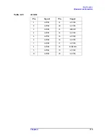
Page 110: ... 13 ACOM 4 ACOM 14 ACOM 5 ACOM 15 ACOM 6 ACOM 16 10MHZ_RF 7 ACOM 17 ACOM 8 ACOM 18 CALOSC_H 9 ACOM 19 CALOSC_L 10 ACOM 20 ACOM Table 2 17 A15J22 Pin Signal Pin Signal 1 ACOM 16 ACOM 2 N15 17 N15 3 N6 18 N6 4 N5 2 19 N5 2 5 P9 20 P9 6 P15 21 P15 7 P32 22 ACOM 8 ACOM 23 ACOM 9 ACOM 24 RF_CK 10 ACOM 25 RF_EN 11 RF_DATA 26 ACOM 12 ACOM 27 ACOM 13 ACOM 28 ACOM 14 P5 2 29 P5 2 15 ACOM 30 ACOM ...

Page 111: ...grams Mnemonics and Connectors Table 2 18 A15J23 Pin Signal Pin Signal 1 ACOM 11 ACOM 2 ACOM 12 ACOM 3 ACOM 13 50MHZ 4 ACOM 14 ACOM 5 ACOM 15 ACOM 6 ACOM 16 ACOM 7 ACOM 17 ACOM 8 ACOM 18 300MHZ 9 ACOM 19 ACOM 10 ACOM 20 ACOM ...

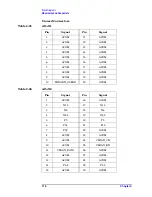
Page 112: ... 14 ACOM 5 ACOM 15 10MHZ_CPU 6 10MHZ_RF 16 ACOM 7 ACOM 17 10MHZ_OPT 8 10MHZ_SYNTH 18 ACOM 9 ACOM 19 10MHZ_AIF 10 ACOM 20 ACOM Table 2 20 A15J32 Pin Signal Pin Signal 1 ACOM 16 ACOM 2 N15 17 N15 3 N6 18 N6 4 N5 2 19 N5 2 5 P9 20 P9 6 P15 21 P15 7 P32 22 P15SBY 8 ACOM 23 ACOM 9 ACOM 24 REF_CK 10 ACOM 25 REF_EN 11 REF_DATA 26 ACOM 12 ACOM 27 ACOM 13 ACOM 28 ACOM 14 P5 2 29 P5 2 15 ACOM 30 ACOM ...

Page 113: ...grams Mnemonics and Connectors Table 2 21 A15J33 Pin Signal Pin Signal 1 ACOM 11 ACOM 2 ACOM 12 ACOM 3 ACOM 13 50MHZ 4 ACOM 14 ACOM 5 ACOM 15 ACOM 6 ACOM 16 ACOM 7 ACOM 17 ACOM 8 ACOM 18 300MHZ 9 ACOM 19 ACOM 10 ACOM 20 ACOM ...

Page 114: ...14 ACOM 5 ACOM 15 ACOM 6 ACOM 16 ACOM 7 ACOM 17 ACOM 8 ACOM 18 ACOM 9 ACOM 19 ACOM 10 MIDGEN_CLEAN 20 ACOM Table 2 23 A15J42 Pin Signal Pin Signal 1 ACOM 16 ACOM 2 N15 17 N15 3 N6 18 N6 4 N5 2 19 N5 2 5 P9 20 P9 6 P15 21 P15 7 P32 22 ACOM 8 ACOM 23 ACOM 9 ABUS 24 SYNTH_CK 10 ACOM 25 SYNTH_EN 11 SYNTH_DATA 26 ACOM 12 ACOM 27 ACOM 13 ACOM 28 ACOM 14 P5 2 29 P5 2 15 ACOM 30 ACOM ...

Page 115: ...nemonics and Connectors Table 2 24 A15J43 Pin Signal Pin Signal 1 ACOM 11 ACOM 2 ACOM 12 ACOM 3 ACOM 13 ACOM 4 ACOM 14 ACOM 5 ACOM 15 10MHZ_SYNTH 6 ACOM 16 ACOM 7 ACOM 17 PRE_LEVEL_DRIVE 8 ACOM 18 ACOM 9 ACOM 19 ACOM 10 ACOM 20 ACOM ...

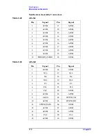
Page 116: ... 5 ACOM 15 ACOM 6 ACOM 16 ACOM 7 ACOM 17 ACOM 8 ACOM 18 ACOM 9 ACOM 19 ACOM 10 MIDGEN_CLEAN 20 ACOM Table 2 26 A15J12 Pin Signal Pin Signal 1 ACOM 16 ACOM 2 N15 17 N15 3 N6 18 N6 4 N5 2 19 N5 2 5 P9 20 P9 6 P15 21 P15 7 P32 22 ACOM 8 ACOM 23 ACOM 9 ACOM 24 CLEAN_CK 10 ACOM 25 CLEAN_EN 11 CLEAN_DATA 26 ACOM 12 ACOM 27 ACOM 13 ACOM 28 ACOM 14 P5 2 29 P5 2 15 ACOM 30 ACOM ...

Page 117: ...OM 12 ACOM 3 ACOM 13 ACOM 4 ACOM 14 ACOM 5 ACOM 15 ACOM 6 ACOM 16 ACOM 7 ACOM 17 ACOM 8 ACOM 18 ACOM 9 ACOM 19 ACOM 10 ACOM 20 ACOM Table 2 28 A15J51 Pin Signal Pin Signal 1 ACOM 11 ACOM 2 ACOM 12 ACOM 3 ACOM 13 NC 4 ACOM 14 ACOM 5 ACOM 15 NC 6 ACOM 16 ACOM 7 ACOM 17 NC 8 ACOM 18 ACOM 9 ACOM 19 NC 10 ACOM 20 ACOM ...

Page 118: ...5 2 5 P9 20 P9 6 P15 21 P15 7 P32 22 ACOM 8 ACOM 23 ACOM 9 ACOM 24 NC 10 ACOM 25 NC 11 NC 26 ACOM 12 ACOM 27 ACOM 13 ACOM 28 ACOM 14 P5 2 29 P5 2 15 ACOM 30 ACOM Table 2 30 A15J53 Pin Signal Pin Signal 1 ACOM 11 ACOM 2 ACOM 12 ACOM 3 ACOM 13 NC 4 ACOM 14 ACOM 5 ACOM 15 NC 6 ACOM 16 ACOM 7 ACOM 17 NC 8 ACOM 18 ACOM 9 ACOM 19 NC 10 ACOM 20 ACOM ...

Page 119: ...Chapter 2 119 Block Diagrams Block Diagrams Block Diagrams ...

Page 120: ...120 Chapter2 Block Diagrams Block Diagrams ...

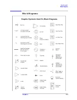
Page 121: ... OUT 250 MHz 4GHz 10dBm W11 W13 P9 P7 IF_IN_SEL IF_SEL BB_SEL P4 PIN62 7 5 MHz 15 dBm Note 1 P8 P4 PIN 27 P4 PIN 55 P4 PIN 54 P4 PIN 29 P4 PIN 23 P4 PIN 25 W2 W1 TO DAUGHTERBOARD P2 PIN 9 A15 P1 J6 P3 P17 ABUS_LOOP ABUS_10V IF RF LO IF RF LO IF RF LO R FRAC N DIVIDE 10 or 12 5 MHz 6 MODULUS CONTROL 4 2 5 x 3 A12 ANALOG IF ASSEMBLY A10 DIGITAL IF ASSEMBLY A27 REAR PANEL I O A15 DAUGHTERBOARD PREFIL...

Page 122: ...122 Chapter2 Block Diagrams Block Diagrams ...

Page 123: ... PROBE POWER EMI FILTER ON_LED KBDREV1 KBDREV1 RPG1A PROBE_N12 6 PROBE_P15 12 6V P1 PROBE POWER ACOM 15V KBDREVO KBDREVO RPG1B DCOM J3 100 PIN FP P155BY FROM A21 MOTHERBOARD P3 40 PIN ACOM VCC VDL P5 2 PROBE_P15 FP_CLCK FP_W_RL FP_PWR_RST_L FP_CSL FP_REDO 3 4 4 4 FP_GREENO 3 FP_BLUEO 3 FP_HSYNCL FP_VSYNCL FP_DOTCLK FP_CBLANKL FP_A3 NOT USED FP_INTRL NOT USED PROBE_N12 6 FP_DATA FP_ADDRESS FP_AO A2...

Page 124: ...124 Chapter2 Block Diagrams Block Diagrams ...

Page 125: ...125 3 Parts List ...

Page 126: ...el information containing material lists schematics and component location diagrams is available separately Refer to the end of this chapter for ordering information The following tables and figures are also included in this chapter Table 3 1 lists reference designator descriptions Table 3 2 lists abbreviations used in the parts list Table 3 3 lists value multipliers Table 3 4 lists replacement pa...

Page 127: ...hin the USA Agilent Technologies can supply parts through a direct mail order system Advantages of using the system are as follows Direct ordering and shipment from Agilent Technologies No maximum or minimum on any mail order There is a minimum order amount for parts ordered through a local Agilent Technologies office when the orders require billing and invoicing Prepaid transportation There is a ...

Page 128: ...s Regular and Hotline Orders The toll free phone number 800 227 8164 is available Monday through Friday 6 a m to 5 p m Pacific time Regular orders have a four day delivery time For after hours there is also a fax number available 800 329 4470 ...

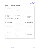
Page 129: ...uit Microcircuit CR Diode Diode Thyristor Step Recovery Diode Varactor M Meter Miscellaneous MP Mechanical Part V Electron Tube DC Directional Coupler VR Breakdown Diode Zener Voltage Regulator DL Delay Line P Electrical Connector Movable Portion Plug DS Annunciator Lamp Light Emitting Diode LED Signaling Device Visible W Cable Wire Jumper Q Silicon Controlled Rectifier SCR Transistor Triode Thyri...

Page 130: ...sic DP3T Double Pole Three Throw BTN Button DPDT Double Pole Double Throw DWL Dowell C E C Capacitance Capacitor Center Tapped Cermet Cold Compression E R E Ring CCP Carbon Composition Plastic EXT Extended Extension External Extinguish CD Cadmium Card Cord CER Ceramic F CHAM Chamfer F Fahrenheit Farad Female Film CHAR Character Characteristic Charcoal F Resistor Fixed Flange Frequency CMOS Complem...

Page 131: ...r MTLC Metallic IF Forward Current Intermediate Frequency MW Milliwatt IN Inch INCL Including N INT Integral Intensity Internal N Nano None N CHAN N Channel J NH Nanohenry J FET Junction Field Effect Transistor NM Nanometer Nonmetallic JFET Junction Field Effect Transistor NO Normally Open Number NOM Nominal K NPN Negative Positive Negative Transistor K Kelvin Key Kilo Potassium NS Nanosecond Non ...

Page 132: ...bleThrow PNL Panel SPST Single Pole SingleThrow PNP Positive Negative Positive Transistor SQ Square POLYC Polycarbonate SST Stainless Steel POLYE Polyester STL Steel POT Potentiometer SUBMIN Subminiature POZI Pozidriv Recess SZ Size PREC Precision PRP Purple Purpose T PSTN Piston T Teeth Temperature Thickness Time Timed Tooth Typical PT Part Point Pulse Time TA Ambient Temperature Tantalum PW Puls...

Page 133: ...ith Dimensions Reactance V V Variable Violet Volt Voltage Y VAC Vacuum Volts Alternating Current YIG Yttrium Iron Garnet VAR Variable VDC Volts Direct Current Z ZNR Zener Table 3 2 Abbreviations Table 3 3 Multipliers Abbreviation Prefix Multiple Abbreviation Prefix Multiple T tera 1012 m milli 10 3 G giga 109 µ micro 10 6 M mega 106 n nano 10 9 k kilo 103 p pico 10 12 da deka 10 f femto 10 15 d de...

Page 134: ... Converter Board E4440 63265 A3 Front Panel Interface Assembly includes Inverter Boards and cables E4406 60007 Prefix US3948 below with CPU assembly E4406 60040 or E4406 60073 A3 Front Panel Interface Assembly includes Inverter Boards and cables E4406 63199 Prefix US4004 MY0000 above or older instruments with CPU assembly E4406 60060 A3A1 A3A2 Inverter Board 2 per instrument 0950 3379 A4 Disk Driv...

Page 135: ...65 E4406 60238 Prefix US3948 below A22A1 128M DRAM Replacement Kit includes replacement standoffs E4406 60053 A22A2 64 MB Flash Memory Replacement Kit includes replacement standoffs E4406 60194 A22A3 GP IB Capacitor Board E4406 60061 Prefix US3948 below A22BT1 CPU Battery Panasonic BR2325 Lithium Polycarbon Monofloride 3V 0 16 AH 1420 0314 A25 SCSI Board with PS 2 keyboard connector E4406 60065 Pr...

Page 136: ...bly E4406 60047 Instrument Label E4406 80009 RPG Knob 0370 3229 Keypad E4406 40010 Line Key push rod E4406 40005 RF Input Bracket E4406 20110 RF Input Connector Type N f to SMA f 1250 1811 Disk Drive Mount E4406 40006 Instrument Cover E4406 00016 Front Frame Assembly E4406 60155a Mid Web E4406 20109 Chassis E4406 00073a Center Web E4406 60054 Cover Disk E4406 00006 Top Brace E4406 00078 Rear Frame...

Page 137: ...Plastic Standoffs 0380 4663 Mid Web Fan Plastic Rivet 0361 1272 Nut W20 2950 0035 Nut A27 2950 0154 Screw M3x0 5 8mm LG Crest Washer Pan Head TORX 0515 0372 Screw M3x0 5 6mm LG Flat Head TORX 0515 1227 Screws Jack 0380 1858 Screwlock Stand Off Hex 0 312 IN LG SCSI 1252 5828 Screw M4x0 7 25mm LG Rear Feet 0515 1619 Washer LK HLC No 10 0 194 IN ID GPIB 2190 0034 Standoff HEX 0 327 IN LG GPIB 0380 06...

Page 138: ...e Flat Flex Disk Drive 8120 8461 W11 Cable Semi Rigid Type M 4 GHz LO E4406 20040a W12 Cable Coax 21 4 MHz RF to Analog IF E4406 60027a W13 Cable Coax 7 5 MHz Digital IF to Analog IF 8120 5022 W19 Cable Coax Type M BNC 321 4 MHz OUT Rear Panel Option 300 E4406 60071a W20 Cable Coax EXT Trig In Rear Panel 8120 5055 W21 W22 Inverter A3 8120 8462 W23 Backlight Top 235 mm 8120 8460 W24 Backlight Botto...

Page 139: ...t Option B7C E4406 60162 W34 Cable Coax Q 14 Input Option B7C E4406 60163 W35 Cable Coax Q 12 Input Option B7C E4406 60164 a For replacement also order Cable Retainer E4400 40002 Snap Ring 0510 1643 Table 3 6 Cables Reference Designator Description Agilent Part Number ...

Page 140: ...el Connector Board A27 J4 Trig 1 Out Part of A27 Rear Panel Connector Board A27 J5 Trig 2 Out Part of A27 Rear Panel Connector Board J22 SCSI Part of the A25 PS2 Board Plus SCSI J23 KEYBD Part of the A25 Digital I O Board P7 Serial Part of A22 CPU Processor Assembly 1252 6672 J13 Monitor Part of A22 CPU Processor Assembly 1252 6671 J14 Parallel Part of A22 CPU Processor Assembly 1252 5706 J12 LAN ...

Page 141: ...0807 A21S1 Power Switch 3101 2976 A22 BT1 CPU Battery Panasonic BR2325 1420 0314 DS1 DS2 Back Light Flat Panel see Figure 3 5 on page 146 0960 1314 For display marked VB02 4 1 mm width tube 2090 0365 For display marked VB01 4 6 mm width tube Rack Mount Kit Contains SYSII slide kit and screws E4406 60115 Service Kit Contains extender boards E4406 60114 ...

Page 142: ...em Description Agilent Part Number 1 Strap Handle Assembly includes the following parts E4400 60026 Screw Machine M5 18 FL TX 0515 0710 2 Bottom Feet 5041 9167 3 Screw M4x0 7 25mm LG 0515 1619 4 Rear Feet 5041 9611 5 Instrument Cover E4406 00016 6 Spring Wire Frame 1460 1345 ...

Page 143: ... 3 143 Parts List Hardware Figure 3 2 Top Brace Hardware Item Description Agilent Part Number 1 Top Brace E4406 00078 2 Screw M3x0 5 8mm LG Crest Washer Pan Head TORX 0515 0372 3 Screw M3x0 5 6mm LG 0515 1227 ...

Page 144: ... Front Panel E4406 60139 5 Front Frame Assembly with EMI gasket and trim strip E4406 60155 6 Line Key push rod Compression Spring Retainer Ring E4406 40005 1460 2580 0510 1055 7 Keyboard E4406 60004 8 Keypad E4406 40010 9 and 11 Dress Panel Assembly E4406 60047 10 Display Bezel Assembly includes E4406 80007 E4406 60046 12 RPG Knob 0370 3229 13 Front Panel Overlay Left non B7C instruments B7C BBIQ ...

Page 145: ...Chapter 3 145 Parts List Hardware Figure 3 4 Front Panel Shield Hardware Item Description Agilent Part Number 1 Screw M3x0 5 8mm LG Crest Washer Pan Head TORX 0515 0372 2 Shield Front E4406 00002 ...

Page 146: ...d 8160 0968 2 A3 Front Panel Interface Assembly includes inverter boards E4406 63199 Prefix US4004 MY0000 above 3 Inverter Boards 0950 3379 4 W6 Cable Flat Flex Flat Panel Interface 8120 8480 5 Backlight Extension Cable Top 235 mm 8120 8460 Bottom 264 mm 8120 8459 6 Backlight For use with display 2090 0396 VB02 display For use with display 2090 0576 VB01 display 0960 1314 2090 0365 7 Screw M3x0 5 ...

Page 147: ...ards under Inverter Shield 0950 3379 3 W6 Cable Flat flex Front Panel Interface to display converter board 8120 1419 4 W27 Cable backlight extension 8121 1420 5 Display Mount E4406 40013 6 Shield Inverter Board E4440 00068 7 Screw M3x0 5 8mm LG Crest Washer Pan Head TORX 0515 0372 8 Display Protector Pressure Plate E4406 00037 9 A2 Flat Panel Display 2090 0897 10 A2A1 Display Converter Board E4440...

Page 148: ...are Item Description Agilent Part Number 1 Screw M3x0 5 8mm LG Crest Washer Pan Head TORX 0515 0372 2 Front Frame Assembly Refer to Table 3 5 3 W8 Cable Front Panel Ribbon 8120 8463 4 W3 Cable Coax Ext Trig In Front Panel E4406 60139 5 Chassis Refer to Table 3 5 ...

Page 149: ...Chapter 3 149 Parts List Hardware Figure 3 8 Bottom Hardware Item Description Agilent Part Number 1 Screw M3x0 5 6mm LG 0515 1227 2 Screw M3x0 5 8mm LG Crest Washer Pan Head TORX 0515 0372 ...

Page 150: ...150 Chapter3 Parts List Hardware Figure 3 9 Disk Drive Parts Item Description Agilent Part Number 1 and 4 Disk Drive Mount E4406 40006 2 Disk Drive 0950 2782 3 Disk Drive Board E4406 60014 ...

Page 151: ...Chapter 3 151 Parts List Hardware Figure 3 10 Disk Drive Chassis Hardware Item Description Agilent Part Number 1 Screw M3x0 5 8mm LG Crest Washer Pan Head TORX 0515 0372 2 Disk Drive Cover E4406 00006 ...

Page 152: ...RF Assembly E4406 60197 3 W20 Cable Coax EXT Trig In Rear Panel 8120 5055 4 Center Web E4406 60054 5 A12 Analog IF Assembly E4440 60029 6 A10 Digital IF Assembly E4440 60195 7 A6 Power Supply Assembly 0950 2797 8 Chassis E4406 00073 9 Rear Frame Assembly and EMI gaskets E4406 60154 10 Dress Panel SCSI E4406 00017 11 Screwlock 1252 5828 12 Rear Dress Panel E4406 00032 ...

Page 153: ...0000 above or instruments retrofitted with CPU upgrade kit E4406 60238 13 A22 CPU Processor Assembly Retrofit Kit includes Front Panel Interface Assembly E4406 60064 and SCSI Board Assembly E4406 60065 E4406 60238 Prefix US3948 below 14 W19 Cable Coax 321 4 MHz OUT Option 300 E4406 60071 Item Description Agilent Part Number ...

Page 154: ...402 below Item Description Agilent Part Number 1 Display EMI Filter 1000 1001 2 Display Mount E4406 40004 3 Flat Panel Display 2090 0396 4 Display Shield Board includes gaskets E4406 60052 5 W24 Cable Backlight Extension Bottom 264 mm 8120 8459 6 W23 Cable Backlight Extension Top 235 mm 8120 8460 ...

Page 155: ...rts List Hardware Figure 3 13 Display Parts Instruments with Serial Prefix US MY46xx above Item Description Agilent Part Number 1 Display EMI Filter 1000 1001 2 Display Mount E4406 40013 3 Flat Panel Display 2090 0897 ...

Page 156: ...rts List Hardware Figure 3 14 Motherboard and Shield Item Description Agilent Part Number 1 Motherboard Shield Assembly E4406 60024 2 Motherboard E4406 60001 3 Screw M3x0 5 8mm LG Crest Washer Pan Head TORX 0515 0372 ...

Page 157: ...apter 3 157 Parts List Hardware Figure 3 15 Center Web Parts Item Description Agilent Part Number 1 W25 Cable Flat Flex Rear Panel I O 8120 8493 2 Screw M3x0 5 8mm LG Crest Washer Pan Head TORX 0515 0372 ...

Page 158: ...nter Web Cables Item Description Agilent Part Number 1 Snap Ring 0510 1643 2 Cable Retainer E4400 40002 W9 Cable Semi Rigid SMA RF Input E4406 20041 W11 Cable Semi Rigid Type M 4 GHz LO E4406 20040 W12 Cable Coax 21 4 MHz RF to Analog IF E4406 60027 ...

Page 159: ...pter 3 159 Parts List Hardware Figure 3 17 Mid Web Parts Item Description Agilent Part Number 1 Screw M3x0 5 8mm LG Crest Washer Pan Head TORX 0515 0372 2 Mid Web E4406 20109 3 Fan Replacement E4406 60159 ...

Page 160: ...Description Agilent Part Number 1 W9 Cable Semi Rigid SMA RF Input E4406 20041 2 Screw M3x0 5 8mm LG Crest Washer Pan Head TORX 0515 0372 3 RF In Attenuator AT1 0955 0807 4 RF Input Bracket E4406 20110 5 RF Input Connector Type N f to SMA f 1250 1811 6 Nut Hex 2950 0154 ...

Page 161: ...Chapter 3 161 Parts List Hardware Figure 3 19 Front Panel External Trigger Connector Hardware Item Description Agilent Part Number 1 Nut W3 2950 0035 ...

Page 162: ...standoffs E4406 60194 3 A22 CPU Processor Assembly does not include A22A1 or A22A2 E4406 60060 Prefix US4004 MY0000 above or instruments retrofitted with CPU upgrade kit E4406 60238 4 Memory Plastic Standoffs 0380 4663 5 Standoff HEX 0 327 IN LG GPIB 0380 0644 8 CPU Bottom Plastic Spacers 0380 4163 9 CPU Battery Panasonic BR2325 Lithium Polycarbon Monofloride 3V 0 16 AH 1420 0314 10 CPU shim 2 E44...

Page 163: ...s Item Description Agilent Part Number 1 W13 Cable Coax 7 5 MHz Digital IF to Analog IF 8120 5022 2 W3 Cable Coax Ext Trig In Front Panel E4406 60139 3 W20 Cable Coax Ext Trig In Rear Panel 8120 5055 4 W12 Cable Coax 21 4 MHz RF to Analog IF E4406 60027 ...

Page 164: ...164 Chapter3 Parts List Hardware ...

Page 165: ...165 4 Assembly Replacement ...

Page 166: ...Introduction Introduction The procedures in this chapter describe the location removal and replacement of major assemblies in your instrument Refer to Chapter 3 Parts List for part numbers assembly descriptions and ordering information ...

Page 167: ... instrument and the general safety considerations at the beginning of this service guide before operating the unit with the cover removed Failure to heed the safety precautions can result in severe or fatal injury Service tools you will need Figure 4 1 TORX Tool After an instrument repair If one or more instrument assemblies have been repaired or replaced perform the related adjustments and perfor...

Page 168: ... A12 Analog IF Assemblies on page 185 A14 Fan Control Board on page 187 A15 Daughter Board on page 189 A17 RF A18 Reference and A19 Synthesizer Assemblies on page 191 Mid Web Fans on page 193 A21 Motherboard on page 198 A22 Processor Assembly on page 202 A22A1 DRAM A22A2 Flash and A22A3 GP IB Capacitor Boards on page 205 A25 SCSI Board on page 207 A27 Rear Panel Connector Board on page 208 Rear Fr...

Page 169: ......

Page 170: ...170 Chapter4 Assembly Replacement Removal and Replacement Procedures ...

Page 171: ...2 There are two handles on the sides of the instrument that must be taken off Refer to Figure 4 2 Using the T 20 driver loosen the screws that attach each handle 1 Remove the handles 3 Remove the four bottom feet 2 This is done by lifting up on the tabs on the feet and sliding the feet in the direction indicated by the arrows 4 Using the T 15 driver remove the four screws 3 that hold the rear feet...

Page 172: ...seats into the gasket groove in the front frame 3 Using the T 15 driver attach the four rear feet with the four screws to the instrument Torque to 21 inch pounds 4 Using the T 20 driver replace the handles Torque to 21 inch pounds 5 Replace the four bottom feet by pressing them into the holes in the case and sliding in the opposite direction of the arrows until they click into place Note that the ...

Page 173: ...efer to the Instrument Outer Case removal procedure 2 Using the T 10 driver remove the 7 top screws 3 and the 10 side screws 2 attaching the top brace 1 to the deck The top screws are different from the side screws Be careful not to mix them Refer to Figure 4 3 3 The top brace can now be removed from the deck Figure 4 3 Top Brace ...

Page 174: ...nt pins and the two alignment holes Make sure that no coaxial cables will get pinched underneath the brace 2 Using the T 10 driver replace the 7 top screws first and then the 10 side screws after the top screws are tightened Torque to 9 inch pounds 3 Replace the outer case Refer to the Instrument Outer Case replacement procedure ...

Page 175: ...sembly 2 to the deck 3 Pull the front frame off of the deck until it is disengaged from the disc drive 4 At this point the front frame can be placed flat on the bench for service while still attached to the instrument If you want to completely remove the front frame continue with the Removal section Removal 1 Using a 9 16 socket drive remove the nut securing the External Trigger Input BNC connecto...

Page 176: ...using a 9 16 socket Torque to 21 inch pounds 4 Clip the coaxial cable into the two cable clamps positioned on the front frame shield 5 Position the front frame on the deck using the alignment bosses on the deck 5 Remember to tuck the ribbon cable under the fans when pushing the frame onto the deck This will insure proper airflow to cool the instrument Using the T 10 driver replace the 6 screws 1 t...

Page 177: ...e A17 A18 and A19 assemblies Refer to A17 RF A18 Reference and A19 Synthesizer Assemblies removal procedure 4 Unplug the ribbon cable from the motherboard 5 Refer to Figure 4 5 Using the T 10 driver remove the 4 screws 1 that attach the disk drive cover 2 to the deck 6 Unplug the flat flex cable from the motherboard and the disk drive connectors It is necessary to unlock these connectors before re...

Page 178: ...178 Chapter4 Assembly Replacement A4 Disk Drive and A5 Disk Drive Board Figure 4 5 Disk Drive Removal Figure 4 6 Disk Drive Board Removal ...

Page 179: ...r to Figure 4 5 Slide the disk drive assembly into the disk shield 4 Plug in the flat flex cable to the disk drive and the motherboard Refer to Figure 4 7 for the proper orientation of the cable 5 Refer to Figure 4 5 Place the disk cover over the ferrite shield Using the T 10 driver replace the 4 screws Torque to 9 inch pounds 6 Plug the ribbon cable onto the motherboard 7 Replace the front frame ...

Page 180: ...oval 1 Remove the instrument top brace Refer to the Top Brace removal procedure 2 Refer to Figure 4 8 Using the T 10 driver remove the 5 screws 1 securing the A6 power supply assembly 2 to the deck and the rear frame 3 Carefully pull up on the power supply assembly to disengage from the motherboard connector Figure 4 8 Power Supply Removal ...

Page 181: ...ower supply assembly into position in the deck Push down to mate the assembly with the motherboard connector 2 Refer to Figure 4 8 Using the T 10 driver replace the 5 screws Torque to 9 inch pounds 3 Replace the instrument top brace Refer to the Top Brace replacement procedure ...

Page 182: ... Step 2 Remove the Baseband I Q Cable Assembly 1 Disconnect the I I Q and Q cables from their respective connectors on the top front of the A7 assembly Each connector is labeled both with the I Q designation and the numerical code of the cable For example the Q connector is labeled Q 14 In Figure 4 9 Item 1 is the Q 14 cable Item 2 is the Q 15 cable Item 3 is the I 12 cable Item 4 is the I 13 cabl...

Page 183: ...ront panel assembly Step 5 Remove the A7 assembly from the instrument 1 Carefully pull up on the baseband I Q assembly ejectors to detach the A7 assembly from the motherboard 2 Unhook the front and rear ejectors under the tabs that are located on the rear frame and mid web of the instrument 3 Slide the A7 assembly out of the front and rear guides of slot 0 Note if the A7 assembly was retrofitted i...

Page 184: ...herboard 3 Hook the front and rear ejectors under the tabs that are located on the rear frame and mid web of the instrument Step 2 Attach the Baseband I Q Cable Assembly 1 Connect the I I Q and Q cables to their respective connectors on the top front of the A7 assembly if they are not already connected 2 Attach the four bundled I Q wires to the cable clip 1400 3014 that is located on the rear of t...

Page 185: ...er to the Top Brace removal procedure 2 Refer to Figure 4 12 Remove the coaxial cables at the locations indicated To remove the A10 digital IF assembly disconnect the cable 1 from the A10 board To remove the A12 analog IF assembly disconnect the cables 1 2 3 and 4 from the A12 board 3 Refer to Figure 4 13 Carefully pull up on the ejectors 1 to disengage the assembly from the connectors and remove ...

Page 186: ...he assemblies Hook the ejectors under the tabs on the rear frame and mid web Carefully push down on the ejectors to mate the assembly with the motherboard connectors 2 Reconnect the coaxial cables that were removed Replace the cables to the correct connectors Refer to the silkscreen on the instrument top brace for correct placement of cables Take care to dress the cables correctly so they aren t p...

Page 187: ...val 1 Remove the instrument top brace Refer to the Top Brace removal procedure 2 The A14 fan control board 1 is attached to the center web by a snap top standoff 2 Refer to Figure 4 14 Carefully pull the fan control board away from the daughter board until it unsnaps from this standoff 3 Pull up on the fan control board to disengage from the motherboard ...

Page 188: ...ement 1 Place the fan control board into position and carefully push down to mate with the motherboard connector 2 Push the top of the fan control board towards the daughter board until it snaps onto the snap top standoffs 3 Replace the instrument top brace Refer to the Top Brace replacement procedure ...

Page 189: ...p brace Refer to the Top Brace removal procedure 2 Remove the A17 A18 and A19 assemblies Refer to the A17 RF A18 Reference and A19 Synthesizer Assemblies removal procedure 3 Refer to Figure 4 15 Unplug the flat flex cable 1 from the rear of the daughter board It is necessary to unlock the connector before removing the cable 4 Using the T 10 driver remove the 6 screws 2 that secure the daughter boa...

Page 190: ...hat secure the daughter board to the center web For alignment purposes tighten the screws marked with a 1 and a 2 marked on the daughter board first then tighten the remaining screws Torque to 9 inch pounds 3 Reconnect the flat flex cable to the daughter board Lock the connector 4 Replace the A17 A18 and A19 assemblies Refer to the A17 RF A18 Reference and A19 Synthesizer Assemblies replacement pr...

Page 191: ...e the same procedures for removal Refer to Figure 4 16 to locate the assembly you wish to replace The A17 RF assembly is identified with 1 A18 reference assembly is 2 and A19 synthesizer assembly is 3 Removal 1 Remove the instrument top brace Refer to the Top Brace removal procedure 2 Carefully pull out on the ejectors 5 located on the assembly you wish to remove Refer to Figure 4 16 3 Slide the a...

Page 192: ...re the removal of a keying tab before it can be inserted into the instrument 2 Place the assembly into the slots on the mid web and rear frame Hook the board ejectors over the vertical tabs 3 Carefully slide the assembly into the daughter board and push on the ejectors to engage the connectors Make certain the rigid cables attached to the center web also engage the assemblies as they are installed...

Page 193: ... procedure 2 Drop the front frame Refer to the Drop the Front Frame procedure 3 Remove the A6 power supply if necessary Refer to the A6 Power Supply removal procedure 4 Remove the A14 fan control board if necessary Refer to the A14 Fan Control Board removal procedure 5 Remove the A17 A18 and A19 boards if necessary Refer to the A17 RF A18 Reference and A19 Synthesizer Assemblies removal procedure ...

Page 194: ...stall the 4 plastic rivets that secure the fan to the mid web With the rivets center posts raised press the rivets through the mid web and into the fan Press down on the center post to snap the rivets into place 3 Replace any assemblies that were removed for access to the fan 4 Plug the fan cables into the motherboard 5 Replace the front frame assembly Refer to the Front Frame replacement procedur...

Page 195: ...procedure 6 Remove the A7 assembly if installed Refer to the A7 Baseband I Q Assembly Option B7C removal procedure 7 Disengage the semi rigid cable from the mid web by removing the RF input bracket from the deck and carefully rotating the cable bracket assembly up Refer to the RF Input Connector removal procedure Using the T 10 driver remove the 2 screws that secure the bracket to the deck 8 Undre...

Page 196: ...e the RF input bracket to the deck with the 2 screws Torque to 9 inch pounds 4 Replace the power supply Refer to the A6 Power Supply replacement procedure 5 Replace the A10 and the A12 assemblies Refer to the A10 Digital IF and A12 Analog IF Assemblies replacement procedure 6 Replace the A7 assembly if installed Refer to the A7 Baseband I Q Assembly Option B7C replacement procedure 7 Replace the A...

Page 197: ...Chapter 4 197 Assembly Replacement Mid Web Fans 10 Replace the instrument top brace Refer to the Top Brace replacement procedure ...

Page 198: ...ference and A19 Synthesizer Assemblies removal procedure 4 Remove the A10 and the A12 assemblies Refer to the A10 Digital IF and A12 Analog IF Assemblies removal procedure 5 Remove the A7 assembly if installed Refer to the A7 Baseband I Q Assembly Option B7C removal procedure 6 Remove the A6 assembly Refer to the A6 Power Supply removal procedure 7 Remove the A22 assembly Refer to the A22 Processo...

Page 199: ...ment A21 Motherboard motherboard 2 to the deck Lift the motherboard out of the deck 13 Refer to Figure 4 21 Remove the shield 1 from the motherboard 2 by removing the 13 screws 3 with the T 10 driver Figure 4 19 Motherboard Removal ...

Page 200: ...200 Chapter4 Assembly Replacement A21 Motherboard Figure 4 20 Bottom Screws Figure 4 21 Motherboard Shield Removal ...

Page 201: ...nch pounds 4 Reattach the W10 flat flex cable and W8 ribbon cable to the motherboard 5 Replace the A15 daughter board center web assembly Refer to the A15 Daughter Board replacement procedure 6 Replace the mid web fan assembly Refer to the Mid Web Fans replacement procedure 7 Replace the A6 assembly Refer to the A6 Power Supply replacement procedure 8 Replace the A22 assembly Refer to the A22 Proc...

Page 202: ...nd replacement procedure After the boards are installed on the new processor board refer to the procedure in Chapter 5 for information on transferring data to the new processor Removal 1 Remove the instrument top brace Refer to the Top Brace removal procedure 2 Remove the A10 assembly Refer to the A10 Digital IF and A12 Analog IF Assemblies removal procedure 3 Remove the A7 assembly if installed R...

Page 203: ...Chapter 4 203 Assembly Replacement A22 Processor Assembly Figure 4 22 Processor Screw Locations Figure 4 23 Processor Assembly Removal ...

Page 204: ...bly flat as you slide it into the deck to avoid damage Fully engage the connectors by pushing on the CPU dress panel 3 Refer to Figure 4 22 Using the T 10 driver secure the assembly to the rear frame with the 14 screws 1 Torque to 9 inch pounds 4 Replace the A25 board Refer to the A25 SCSI Board replacement procedure 5 Replace the A10 assembly Refer to the A10 Digital IF and A12 Analog IF Assembli...

Page 205: ...move the A22 assembly Refer to the A22 Processor Assembly removal procedure 3 Refer to Figure 4 24 Pinch the standoffs and carefully pull up on either the A22A1 DRAM board 1 or the A22A2 Flash board 2 to disengage it from the processor assembly 4 Instruments with serial prefix US3948 and below also have the A22A3 GP IB capacitor board To remove the A22A3 GP IB capacitor board 3 carefully pull up o...

Page 206: ...earlier A22 CPU assembly with a newer one E4406 60060 the GP IB capacitor board is not required Discard the old A22A3 assembly and proceed to step 3 If you have an earlier A22 CPU assembly insert the GP IB capacitor board into the J8 connector on the processor board and press down to seat Make sure the board is fully seated in the connector to avoid shorting to the deck 3 Replace the A22 assembly ...

Page 207: ...he rear frame and will not come out using the flat blade screwdriver remove the 2 screwlocks 2 that secure the dress panel 3 to the A25 board Figure 4 25 SCSI Board Removal Replacement 1 Replace the A25 board by inserting it into the opening on the rear frame Carefully position the board in the CPU board connector and push down to mate 2 Replace the panel onto the frame by replacing the 7 screws u...

Page 208: ...ve the top brace Refer to the Top Brace removal procedure 3 Remove the A17 A18 and A19 assemblies Refer to A17 RF A18 Reference and A19 Synthesizer Assemblies removal procedure 4 Disconnect the ribbon cable from the daughterboard 5 Refer to Figure 4 26 Using the 9 16 open end wrench remove the four nuts 1 that secure the rear panel connectors to the rear frame 6 Using the T 10 driver remove the 13...

Page 209: ...er replace the 13 screws to secure the rear dress panel to the rear frame For alignment purposes tighten the screws silkscreened with a 1 and a 2 first Torque to 9 inch pounds 3 Reconnect the ribbon cable to the daughterboard 4 Replace the A17 A18 and A19 assemblies Refer to A17 RF A18 Reference and A19 Synthesizer Assemblies replacement procedure 5 Replace the top brace Refer to the Top Brace rem...

Page 210: ...the A7 assembly if installed Refer to the A7 Baseband I Q Assembly Option B7C removal procedure 5 Remove the A25 SCSI board Refer to the A25 SCSI Board removal procedure 6 Remove the A22 processor assembly Refer to the A22 Processor Assembly removal procedure 7 Detach the flat flex cable from the daughter board 8 Remove the rear dress panel which includes the rear panel connector board and the Ext...

Page 211: ...kscreened on the dress panel first Torque to 9 inch pounds 4 Re attach the flat flex cable from the daughter board to the rear panel connector board 5 Replace the A22 processor assembly Refer to the A22 Processor Assembly replacement procedure 6 Replace the A25 SCSI board Refer to the A25 SCSI Board replacement procedure 7 Replace the A10 and the A12 assemblies Refer to the A10 Digital IF and A12 ...

Page 212: ... 1 Use the snap ring tool to separate the snap ring and remove it from the cable retainer 6 Once the snap ring is removed the cable and cable retainer 2 can be pulled away from the center web To remove the 21 4 MHz cable W12 it is necessary to disconnect the cable from the A10 analog IF assembly To remove the RF input cable W9 it is also necessary to disconnect the cable from the input connector a...

Page 213: ...Chapter 4 213 Assembly Replacement Center Web Cables W9 W11 and W12 11 Replace the instrument top brace Refer to the Top Brace replacement procedure Figure 4 28 Center Web Cable Removal ...

Page 214: ...Refer to Figure 4 29 Using a 5 16 inch wrench disconnect the semi rigid cable 1 from the attenuator connector 4 Using the T 10 driver remove the 2 screws 2 that secure the input connector bracket to the deck 5 Remove the attenuator connector from the instrument 6 Separate the attenuator 3 from the input connector 5 using a 5 16 inch wrench 7 Remove the connector from the bracket 4 using a 9 16 inc...

Page 215: ...ment 4 Using the T 10 driver replace the 2 screws that secure the input connector bracket to the deck Torque to 9 inch pounds 5 Using a 5 16 inch wrench reconnect the semi rigid cable to the attenuator connector To avoid twisting the cable hold onto it during tightening Torque to 10 inch pounds 6 Replace the front frame Refer to the Front Frame replacement procedure 7 Replace the instrument outer ...

Page 216: ...cable clamps Using the T 10 driver remove the 11 screws 1 securing the front shield 2 to the front frame Lift the shield from the front frame After the subassembly is changed replace the front shield using the 11 screws removed earlier For alignment purposes tighten the screws marked with 1 and 2 first silkscreened on the shield then tighten the remaining screws Torque to 9 inch pounds Reconnect t...

Page 217: ...gure 4 31 Front Frame Subassemblies The front frame assembly consists of the following sub assemblies Item Description 1 Display Shield Borad 2 Front Panel Interface Board 3 Inverter Boards 4 Display Ribbon Cable 5 Backlight Extension Cables 6 Backlight Connectors ...

Page 218: ...ription 1 Display Assembly 2 Front Shield 3 Front Panel Interface Assembly 4 W3 Cable Coax Ext Trig In Front Panel 5 Front Frame Assembly 6 Line Key push rod 7 Keyboard 8 Keypad 9 and 11 Dress Panel Assembly 10 Display Bezel Assembly includes E4406 80007 12 RPG Knob 13 Front Panel Overlay Left 14 Plug Hole Nylon 15 Name Plate Overlay ...

Page 219: ... Backlights and Filter Figure 4 33 Display Parts Refer to Figure 4 33 The display assembly consists of Item Description 1 EMI filter 2 display mount 3 LCD with backlights 4 Display shield board 5 Backlight extension cable bottom 6 Backlight extension cable top 7 Backlight ...

Page 220: ...31 Unplug the backlight extension cables 5 from the backlight connectors 6 and pull the cables out of the rubber display mount Carefully lay these cables away from the display 2 Unplug the display flat flex cable 4 from the display connector To do this you must first pull up on both sides of the locking mechanism of the ribbon cable connector 3 Remove the rubber mount that houses the display assem...

Page 221: ...nt into position in the front frame assembly as shown in Figure 4 31 5 Plug the flat flex cable into the display connector Push down on both sides of the locking mechanism 6 Refer to Figure 4 31 Connect the backlight extension cables 5 to the backlight connectors 6 Press the backlight extension cables into the grooves in the rubber flaps Make sure the white wire of the backlight connector is on to...

Page 222: ... display Carefully pull on the tab on the backlight assembly 2 to slide the backlight partially out of the display Once the end of the backlight casing is exposed you can pull it straight out from the display NOTE Do not touch the bulb encased in the plastic backlight assembly 4 Insert the new backlight assembly 2 by sliding it into the display non wired end first taking care not to force it It is...

Page 223: ...lip the display mount assembly over and place it filter side up on a flat surface 3 The display filter can now be removed by pulling back on one of the corner supports 2 and lifting the filter 1 out of the mount as shown in Figure 4 36 4 When you install a new filter take care to touch only the outside edges Install the filter into the mount by sliding under the corner supports NOTE Make sure the ...

Page 224: ...nplug the display flat flex cable 4 from the front panel interface board To do this you must first pull up on both sides of the locking mechanism of the ribbon cable connector If not carefully inserted display problems may result 4 Using the T 10 driver remove the 7 screws 1 that secure the front panel interface board 5 to the front frame assembly 5 Lift the front panel interface board from the fr...

Page 225: ...tor with the connector in the keyboard 2 Using the T 10 driver replace the 7 screws that secure the board to the front frame Torque to 9 inch pounds 3 Plug the display flat flex cable into the front panel interface board connector Push down on both sides of the locking mechanism 4 Reconnect both of the 2 wire backlight cables 5 Press the RPG knob onto the control shaft ...

Page 226: ...ure 4 39 The 10 screws also attach the dress panel bezel subpanel keypad and keyboard to the front frame Take care to keep these parts in the correct order and aligned properly 5 Lift the front frame off of the keypad keyboard assembly 6 The bezel and keyboard can now be separated by pressing on the pin just above the On Standby LEDs on the bezel and sliding apart to unlock the tabs The flexible k...

Page 227: ...Chapter 4 227 Assembly Replacement Front Frame Subassemblies Figure 4 39 Keypad Parts ...

Page 228: ... 39 Place the keyboard bezel assembly face down on top of the dress panel and subpanel on a flat surface Install the front frame over the keyboard bezel assembly Using the T 10 driver replace the 10 screws 1 that secure the bezel and keypad to the front frame Torque to 9 inch pounds 4 Replace the front panel interface board Refer to the A3 Front Panel Interface Board replacement procedure 5 Replac...

Page 229: ...he A3 Front Panel Interface Board removal procedure 2 Unsolder the RPG remove the nut and washer and remove it from the front panel interface board 3 Place the new RPG in the correct position tighten the nut and washer and resolder the leads 4 Replace the front panel interface board Refer to the A3 Front Panel Interface Board replacement procedure ...

Page 230: ...16 socket remove the nut 1 that secures the connector to the front frame 3 Disconnect the cable from the A12 analog IF assembly 4 For replacement position the connector cable through the front frame 5 Using the 9 16 socket replace the nut to secure the connector to the front frame Torque to 21 inch pounds 6 Clip the cable into the cable clamps on the shield 7 Re route the cable to avoid interferen...

Page 231: ...231 5 Post Repair Procedures ...

Page 232: ... The following sections are found in this chapter Before You Start on page 233 Abnormal Indications during Procedure Execution on page 233 After Assembly Replacement on page 233 Post Repair Procedures on page 234 Test equipment you will need on page 236 Manual Test Adjustment and Configuration Procedures on page 237 External Keyboard Test on page 239 Configuring a Replacement CPU Assembly on page ...

Page 233: ...e Read the rest of this section Abnormal Indications during Procedure Execution If the indications received during a procedure execution do not agree with the normal conditions given in the procedure a fault exists in your instrument The fault should be repaired before proceeding with any further procedures Refer to the troubleshooting and repair information in Chapter 1 of this guide After Assemb...

Page 234: ...nstrument specifications or the software for information on instrument warm up before performing any of the procedures listed in this chapter Table 5 1 Post Repair Testing Requirements Assembly Adjustments Tests Configuration Performance Verification A1 Keyboard Front Panel test Refer to Internal Front Panel Test on page 238 None A2 Flat Panel Display Ensure that the display quality is satisfactor...

Page 235: ...ck front panel power switch operation Check for proper fan operation and direction of rotation rear exhaust on power up If satisfactory allow the instrument to warm up Check probe power connector voltages Upon warm up ensure the red LEDs on the board are not turned on These signal an over temperature condition when lit None A15 Daughter Board Power instrument up and check for proper operation Chec...

Page 236: ...o Synthesizer Adjustment Number One Phase Noise Spurious Responses Residual FM A21 MotherBoard None None A22 CPU processor Assembly Configuring a Replacement CPU Assembly on page 241 None A22A1 DRAM Card None None A22A2 Flash Memory Board Configuring a Replacement Flash Memory Assembly on page 244 Synthesizer Adjustment Number Two Phase Noise A25 SCSI Board External Keyboard Test on page 239 None ...

Page 237: ... steps necessary to complete the procedure They are designed to be run on an instrument operating within a temperature range of 20 C to 30 C The following is a list of the procedures included in this section Internal Front Panel Test on page 238 External Keyboard Test on page 239 Configuring a Replacement CPU Assembly on page 241 Configuring a Replacement Flash Memory Assembly on page 244 Internal...

Page 238: ... that originally appeared to the right of the key column Each additional instance of pressing a given key will result in an increment to the number listed in the column to the right of the key description For example if you press the Zoom key four times you will see a 4 to the right of the Zoom entry Rotating the RPG knob will result in a rapidly incrementing or decrementing value appearing in the...

Page 239: ... shown as front_panel perform the following steps to verify keyboard operation 1 Connect a PS2 keyboard 2 Reboot the instrument and watch the instrument display 3 When the message To discontinue press any key within 2 seconds appears press any front panel numeric key 0 9 4 Backspace to clear any characters you may have typed after the prompt Main Menu Enter Command 5 From the instrument front pane...

Page 240: ... the keyboard path is shown as PS2 perform the following steps to verify keyboard operation 1 Connect a PS2 keyboard 2 To confirm the operation of the external keyboard perform the following steps a Reboot the instrument and watch the instrument display When the message To discontinue press any key within 2 seconds appears press the space bar on the external key board to interrupt the boot process...

Page 241: ...instrument serial number press System More until 2 of 3 is displayed and Show System Refer to the note below before proceeding a Confirm that the serial number on screen matches the number on the rear panel tag b If the instrument is not functional use the serial number on the rear panel tag NOTE The serial number stored in memory is used to enable all licensed options If the stored serial number ...

Page 242: ...ng the Flash memory board from the defective processor board will save time otherwise required to reconfigure Transferring all three will help keep repair cost low Refer to assembly replacement procedure A22 Processor Assembly on page 202 for details on replacing the defective main processor board and transferring the two memory boards and the GP IB capacitor board Entering Configuration Informati...

Page 243: ...ber from the front panel 2 Press Serial Number alpha editor will be activated and carefully enter the serial number If you make an error press Backspace For an explanation of the use of the alpha editor refer to Using the Alpha Editor Menu on page 258 3 Then press Done to write the serial number to the instrument memory Entering the Time and Date 1 Press System Time Date Set Time and enter the tim...

Page 244: ...ense key number has been issued The synthesizer calibration data LO tuning constants MHZ volt tuning sensitivities are obtained by performing Synthesizer Adjustment Number Two The replacement Flash memory assembly will already have the operating system and firmware installed The license key numbers for each option must be reloaded to enable the option If possible it is best to capture this informa...

Page 245: ...s loaded type BAC and press Done The key number will appear on the License Key Then press Choose Option to view additional options b To determine if the BAH GSM option is loaded type BAH and press Done The key number will appear on the License Key Then press Choose Option to view additional options NOTE If the instrument is not functional contact the owner for the license key numbers The user s gu...

Page 246: ... have completed entering the license key number press the Done key For more information on the alpha editor refer to Using the Alpha Editor Menu on page 258 NOTE It is very important to enter the number accurately Since it is a hexadecimal the letter O can not be present only zeros 0 are used in the license key number 3 After you have entered the active license key number and the personality optio...

Page 247: ...nt user will need to re enter the IP address and host name into the instrument memory The procedure to reenter this information can be found below and in the Configuring I O section in the user s guide 1 To enter the IP address press System Config I O IP Address enter the numeric IP address and press Enter 2 To enter the host name press System Config I O and Host Name Pressing the Host Name key ac...

Page 248: ...uires a minimum of a 24 hour warmup time The UUT must be turned on not in standby for the entire warmup period Required Equipment The following table lists the test equipment required for the adjustment The list includes any miscellaneous devices cables and adaptors Refer to Table 1 2 Required Test Equipment Summary on page 18 for the critical specifications of the test equipment Table 5 2 Require...

Page 249: ...ress MODE and Service 4 Press FREQUENCY 10 and MHz 5 Ensure that a 10 MHz signal appears on the display 6 Press System More until 2 of 3 is displayed Show System Service Password 7378423 and Enter 7 Press MEASURE Timebase Frequency AMPLITUDE Scale Div 60 mV Meas Setup and Auto Adjust Now The Auto Adjust Now does not highlight An indicator of a proper adjustment is Adjusting 1 displayed in the lowe...

Page 250: ...or is used when the instrument performs many of the auto alignment measurements NOTE Ensure that the UUT has been warmed up in accordance with the instrument specifications Required Equipment The following table lists the test equipment required for the adjustment The list includes any miscellaneous devices cables and adaptors Refer to Table 1 2 Required Test Equipment Summary on page 18 for the c...

Page 251: ...stment Figure 5 2 Source Adjustment Setup Figure 5 3 Internal 50 MHz Calibration Adjustment Setup Procedure 1 Preset the power meter CAUTION When using the 8481D Power Sensor a 30 dB fixed attenuator must be Power Sensor Cable 11730A Table 5 3 Required Test Equipment Continued Instrument Recommended Agilent Model Number Alternative Agilent Model Number ...

Page 252: ...5 4 Signal Source Initialization on page 252 5 Adjust the source amplitude until the power meter reads 25 dBm 0 2 dBm 6 Record the measured value from the power meter ___________ dBm NOTE Do not readjust the source amplitude during the remainder of the test 7 Configure equipment as shown in Figure 5 3 Internal 50 MHz Calibration Adjustment Setup 8 Press Preset 9 If the auto alignment for the UUT h...

Page 253: ...omplete the alignment by performing the following steps a Press System More until 2 of 3 is displayed Show System Service Password 7378423 and Enter b Press System Alignments Align Subsystem and Align 50 MHz Reference c Press RF Inp Lev enter the amplitude value recorded from the power meter reading in step 7 and press dBm d Press Adjust Now and wait for the routine to complete e Press Store Abs A...

Page 254: ... displayed on the RF Envelope window and will appear as an unsynchronized signal When the RF Burst trigger function is activated the RF train will sync on the burst trigger signal Procedure 1 Press Preset 2 Press MODE and Service 3 Press Input Input Port IF Align IF Align Signal Signal Type and Pulse The unsynchronized pulse train will be displayed on the RF Envelope window 4 Press Meas Setup Trig...

Page 255: ...for all input connector and impedance settings Procedure 1 Press Mode then Basic to select the Basic mode for the UUT 2 Press Preset to preset the UUT 3 If the auto alignment for the UUT has not been run within the last hour press System Alignment then Align All Now to activate the alignment 4 Initialize the parameters for the instrument as listed in Table 5 6 by following these steps a Press Inpu...

Page 256: ...input for I is I and for Q is Q e Press Marker Search f Record the measured value in the UUT Measured Amplitude column for 100 kHz in Table 5 8 g Compare the measured and nominal values to ensure that the measured value is within the 1dB test limit 7 Press SPAN 5 then MHz to change the span of the UUT 8 Change the signal source frequency to 5 MHz 9 Repeat step 6 and record the measured value in th...

Page 257: ... input 16 1 0 Q only 600 Ω Balanceda 1 Q input 22 1 0 Q only 1 MΩ Unbalanced 1 Q input 10 1 0 Q only 1 MΩ Balanceda 1 Q input 10 1 0 Q only 1 MΩ Balanceda 1 Q input Q bar 10 1 0 a Whenever performing a balanced measurement ensure the complimentary input is terminated for a balanced input when the signal source is connected to the I input the I input must be terminated Table 5 8 Amplitude Accuracy ...

Page 258: ...til 2 of 3 is displayed To access mathematical symbols and punctuation marks press More until 3 of 3 is displayed 3 Press Return to return to the previous menu without entering characters 4 To enter a space press Space which is available on both the letters and the symbols menus 5 If you need to correct a character you have entered you can use the backspace key to move the cursor in the active fun...

Page 259: ...appeared to the right of the key column Each additional instance of pressing a given key will result in an increment to the number listed in the column to the right of the key description For example if you press the Zoom key four times you will see a 4 to the right of the Zoom entry Rotating the RPG knob will result in a rapidly incrementing or decrementing value appearing in the column to the ri...

Page 260: ...s pressed indicator You will see a count of the number of times you have pressed a key next to that key on the display except for the knob next to which you will see positive or negative numbers in increments of 1 Troubleshooting Hints If the front panel check fails contact the Agilent Technologies instrument support center See Table 1 5 on page 61 ...

Page 261: ...N7812A Calibration Application Software performs automated adjustments Brief descriptions and setups for the automated adjustment procedures is found in the software itself Details about the computer and test equipment requirements needed to run the software can be found in Table 1 2 on page 18 ...

Page 262: ...262 Chapter5 Post Repair Procedures Automated Adjustments ...

Page 263: ...ections 81 part number 134 removal 191 troubleshooting 52 A2 flat panel display block description 86 removal 220 troubleshooting 28 A21 fan control board connector mnemonics 99 A21 mother board block description 84 connector mnemonics 92 part number 134 removal 198 A22 processor assembly block description 82 connector mnemonics 107 108 109 part number 134 removal 202 troubleshooting 54 A22A1 DRAM ...

Page 264: ...ring host name 247 IP address 247 serial number 243 entering configuration information 242 equipment adjustments 18 performance verification tests 18 ESD Information 15 Ethernet Addr key 247 external keyboard test description 239 external monitor 28 external trigger front panel connector removal 230 F fan control board see A14 fan control board fan voltages 27 fans removal 193 fans troubleshooting...

Page 265: ... rear panel connectors 54 reference adjustment test description 248 reference assembly see A18 reference assembly reference designators 129 reference unlock detector description 79 removal procedures 168 remove see individual assemblies replace see individual assemblies replaceable parts 134 replacement procedures 168 replacement processor 54 replacing assemblies see individual assemblies 168 requ...

Page 266: ... test failures 58 problems at power up 25 see individual assemblies symptoms 24 U uninstalling measurement personalities 246 unused daughter board connectors connector mnemonics 116 updating firmware 63 URL 23 60 V variable gain amplifier description 73 VCO 52 VCO phase lock loop description 80 VCXO 50 VGA monitor 28 VSYNC troubleshooting 30 W web site URL 23 X XTAL filter mode 43 XTAL prefilter n...

Reviews: