88
Chapter 2
Block Diagrams
Mnemonics and Connectors
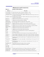
FLOPPY_DS3L
Drive select #3 signal from the floppy controller chip on the CPU board to the floppy drive
FLOPPY_HSL
Head select signal from the floppy controller chip on the CPU board to the floppy drive
FLOPPY_IDXL
Index signal from the floppy drive to the floppy controller chip on the CPU board
FLOPPY_MID
FLOPPY_RDDL
Read disk data from the floppy drive to the floppy controller chip on the CPU board
FLOPPY_READY
FLOPPY_STEPL
Step pulse signal from the floppy controller chip on the CPU board to the floppy drive
FLOPPY_TR00L
Track 00 status signal from the floppy drive to the floppy controller chip on the CPU board
FLOPPY_WDL
Write data signal from the floppy controller chip on the CPU board to the floppy drive
FLOPPY_WEL
Write enable signal from the floppy controller chip on the CPU board to the floppy drive
FLOPPY_WPL
Write protect signal from the floppy drive to the floppy controller chip on the CPU board
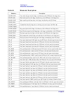
FP_A0
Front panel bus address 0 (LSB) signal from the CPU board to the front panel interface board
FP_A1
Front panel bus address 1 signal from the CPU board to the front panel interface board
FP_A2
Front panel bus address 2 signal from the CPU board to the front panel interface board
FP_A3
Front panel bus address 3 signal from the CPU board to the front panel interface board
FP_BLUE0
Flat panel display blue 0 (LSB) signal from the CPU board to the front panel interface board
FP_BLUE1
Flat panel display blue 1 signal from the CPU board to the front panel interface board
FP_BLUE2
Flat panel display blue 2 signal from the CPU board to the front panel interface board
FP_BLUE3
Flat panel display blue 3 (MSB) signal from the CPU board to the front panel interface board
FP_CBLANKL
Flat panel display blanking signal from the CPU board to the front panel interface board
FP_CLK
Front panel bus 7.5 MHz clock signal from the CPU board to the front panel interface board
FP_CSL
Front panel bus chip select signal from the CPU board to the front panel interface board
FP_D0
Front panel bus data 0 (LSB) signal from the CPU board to the front panel interface board
FP_D1
Front panel bus data 1 signal from the CPU board to the front panel interface board
FP_D2
Front panel bus data 2 signal from the CPU board to the front panel interface board
FP_D3
Front panel bus data 3 signal from the CPU board to the front panel interface board
FP_D4
Front panel bus data 4 signal from the CPU board to the front panel interface board
FP_D5
Front panel bus data 5 signal from the CPU board to the front panel interface board
FP_D6
Front panel bus data 6 signal from the CPU board to the front panel interface board
FP_D7
Front panel bus data 7 (MSB) signal from the CPU board to the front panel interface board
FP_DOTCLK
Flat panel display 25 MHz dot clock signal from the CPU board to the front panel interface board
FP_GREEN0
Flat panel display green 0 (LSB) signal from the CPU board to the front panel interface board
FP_GREEN1
Flat panel display green 1 signal from the CPU board to the front panel interface board
Table 2-1
Mnemonic Descriptions
Mnemonic
Description
Summary of Contents for E4406A VSA Series
Page 4: ...4 ...
Page 10: ...10 Contents ...
Page 11: ...11 1 Troubleshooting ...
Page 66: ...66 Chapter1 Troubleshooting How to Return Your Instrument for Service ...
Page 67: ...67 2 Block Diagrams ...
Page 119: ...Chapter 2 119 Block Diagrams Block Diagrams Block Diagrams ...
Page 120: ...120 Chapter2 Block Diagrams Block Diagrams ...
Page 122: ...122 Chapter2 Block Diagrams Block Diagrams ...
Page 124: ...124 Chapter2 Block Diagrams Block Diagrams ...
Page 125: ...125 3 Parts List ...
Page 164: ...164 Chapter3 Parts List Hardware ...
Page 165: ...165 4 Assembly Replacement ...
Page 169: ......
Page 170: ...170 Chapter4 Assembly Replacement Removal and Replacement Procedures ...
Page 227: ...Chapter 4 227 Assembly Replacement Front Frame Subassemblies Figure 4 39 Keypad Parts ...
Page 231: ...231 5 Post Repair Procedures ...
Page 262: ...262 Chapter5 Post Repair Procedures Automated Adjustments ...


