5-8
Service Guide E8364-90001
Theory of Operation
PNA Series Microwave Network Analyzers
Source Group Operation
E8362A, E8363A, E8364A
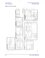
At the output, an ALC circuit maintains the power level at
−
5 dBm
±
2 dB for bands 1–2 or
−1.
5 dBm
±
2 dB for bands 3–25. In all bands, the output is sent to the A17–A20 LO
distribution path and on to the A27–A30 first converters, as the 1st LO signal.
A17 L.O. Multiplier/Amplifier 10 (LOMA 10)
In bands 1–3, the input signal from the A8 fractional-N synthesizer board is passed
through the A17 LOMA 10 unchanged. For all other bands, the signals are doubled,
filtered, and amplified. In bands 8–10, 12–19, and 21–25, the signals are again doubled,
filtered, and amplified. Together, all of these signal paths create the full output frequency
range of 53 MHz to 10 GHz.
A18 Multiplier/Amplifier 20 (MA 20)
In bands 1–10 and 16–18, the 53 MHz to 10 GHz input frequencies are filtered, amplified,
and passed through the A18 MA 20. In bands 11–15, and 19–25, the signals are doubled,
filtered, and amplified.
Together, these signal paths create the full output frequency range of 53 MHz to 20 GHz
that is sent to the A19 splitter.
A19 Splitter
The A19 splitter receives the 53 MHz to 20 GHz LO signal from the A8, A17, and A18 LO
generation chain and divides it into two signals which are routed to the A20 L.O.
distribution assembly (LODA). This splitter configuration provides the highest level of
balance and control of the LO signal.
A20 L.O. Distribution Assembly (LODA)
In the A20 LODA, the LO signal is amplified and split to provide balanced LO signals to
each of the A27–A30 receiver first converters.
A10 Frequency Reference Board
This assembly provides stable reference frequencies to the rest of the instrument. A high
stability 10 MHz oven-controlled crystal oscillator (OCXO) normally provides the
frequency standard. However, if a 10 MHz external reference signal is detected at the
10 MHz EXT REF IN port on the rear panel, it is used as the frequency reference instead.
The 10 MHz reference signal is used to phase lock a 100 MHz VCO. This VCO is then used
to phase lock a second VCO at 99.5 MHz. It is also used to provide the 10 MHz EXT REF
OUT rear panel signal, reference for the A11 phase lock board, and a 5 MHz reference for
the A6 signal processing ADC module (SPAM) board and the A8 fractional-N synthesizer
board.
The 95.5 MHz reference signal is sent through a divide-by-3 circuit to produce the fourth
multiple of the 8.29167 MHz 2nd LO signal which is sent to the A35 receiver motherboard.
The 100 MHz reference signal is sent through a divide-by-12 circuit to produce the
8.3333 MHz phase lock reference signal which is sent to the A11 phase lock board.
Summary of Contents for E8362A
Page 11: ...Service Guide E8364 90001 1 1 1 Safety and Regulatory Information ...
Page 19: ...Service Guide E8364 90001 2 1 2 General Product Information ...
Page 29: ...Service Guide E8364 90001 3 1 3 Tests and Adjustments ...
Page 79: ...Service Guide E8364 90001 4 1 4 Troubleshooting ...
Page 139: ...Service Guide E8364 90001 5 1 5 Theory of Operation ...
Page 169: ...Service Guide E8364 90001 6 1 6 Replaceable Parts ...
Page 215: ...Service Guide E8364 90001 7 1 7 Repair and Replacement Procedures ...
Page 287: ...Service Guide E8364 90001 A 1 A Error Terms ...
Page 303: ...Service Guide E8364 90001 B 1 B Option Enable Utility ...
Page 309: ...Service Guide E8364 90001 C 1 C Firmware Upgrades ...
Page 313: ...Service Guide E8364 90001 D 1 D Operating System Recovery ...


