background image

7-18

Service Guide E8364-90026

Repair and Replacement Procedures

PNA Series Microwave Network Analyzers

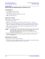
Removing and Replacing the A6, A8, A9, and A10 Boards

E8362B, E8363B, E8364B

Removing and Replacing the A6, A8, A9, and A10 Boards

Tools Required 

• T-10 TORX driver (set to 9 in-lb) 

• T-20 TORX driver (set to 21 in-lb)

• ESD grounding wrist strap

Removal Procedure

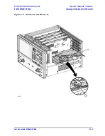
Refer to 

Figure 7-7

 for this procedure.

1. Disconnect the power cord.

2. Remove the outer and inner covers. Refer to 

“Removing the Covers” on page 7-6

.

3. With a T-10 TORX driver, remove the two brackets that secure cables to the top of the 

midweb.

4. Identify the board you want to remove and disconnect any cables that are attached to it.

5. Lift the two extractors (item 

), located at each end of the board.

NOTE

Before removing the board completely, check the bottom of the board for any 
attached cables. 

6. While holding on to the extractors, slide the board out of the slot and remove it from the 

analyzer.

Replacement Procedure

1. Reverse the order of the removal procedure.

2. Perform the post-repair adjustments, verifications, and performance tests that pertain 

to this removal procedure. Refer to 

Table 7-2 on page 7-80

Summary of Contents for E8362B

Page 1: ...ervice Guide E8362B E8363B E8364B Agilent Technologies PNA Series Microwave Network Analyzers Part Number E8364 90026 Printed in USA November 2008 Supersedes March 2008 Agilent Technologies Inc 2002 2008 ...

Page 2: ...act Software is delivered and licensed as Commercial computer software as defined in DFAR 252 227 7014 June 1995 or as a commercial item as defined in FAR 2 101 a or as Restricted computer software as defined in FAR 52 227 19 June 1987 or any equivalent agency regulation or contract clause Use duplication or disclosure of Software is subject to Agilent Technologies standard commercial license term...

Page 3: ...miliarize yourself with each of the notes and its meaning before operating this instrument All pertinent safety notes for using this product are located in Chapter 1 Safety and Regulatory Information WARNING Warning denotes a hazard It calls attention to a procedure which if not correctly performed or adhered to could result in injury or loss of life Do not proceed beyond a warning note until the ...

Page 4: ...a presentation and access the analyzer s Web page The Installation and Quick Start Guide helps you to quickly familiarize yourself with the analyzer Procedures are provided for installing configuring and verifying the operation of the analyzer Printing Copies of Documentation from the Web To print copies of documentation from the Web download the PDF file from the Agilent web site Go to www agilen...

Page 5: ...ncy Range to 50 GHz 2 4 Option 067 and 068 Extended Frequency Range to 67 GHz 2 4 Option 080 Frequency Offset Mode 2 4 Option 081 External Reference Switch 2 5 Option 083 Frequency Converter Measurement Application 2 5 Option 099 Firmware Upgrade 2 5 Option 221 2 Port Front Panel Upgrade 2 5 Option 897 Built In Tests for Commercial Calibration 2 5 Option 898 Built In Tests for Standards Compliant ...

Page 6: ...System Verification Verifies 3 20 Measurement Uncertainty 3 21 Measurement Traceability 3 22 Performing System Verification 3 23 Option H11 IF Access Operation Verification 3 30 Performance Tests Agilent N7840A Software Package 3 31 Source Power Accuracy Test 3 31 Source Maximum Power Output Test 3 32 Source Power Linearity Test 3 32 Frequency Accuracy Test 3 33 Trace Noise Test 3 33 Receiver Comp...

Page 7: ...p 4 35 Checking the Signal Separation Group 4 48 Checking the Receiver Group 4 52 Checking the Frequency Offset Group Option 080 4 54 Instrument Block Diagrams 4 60 E8362B Overall Block Diagram No Options 4 60 E8362B Overall Block Diagram All Options 4 62 E8363B and E8364B Overall Block Diagram No Options 4 64 E8363B and E8364B Overall Block Diagram All Options 4 66 5 Theory of Operation Informati...

Page 8: ...r Panel Connections 5 26 Digital Processing and Digital Control Group Operation 5 29 Front Panel Subgroup 5 31 Data Acquisition and Processing Subgroup 5 32 Power Supply Group Operation 5 34 6 Replaceable Parts Information in This Chapter 6 2 How to Use the Replaceable Parts Listings in This Chapter 6 2 Chapter Six at a Glance 6 2 Ordering Information 6 3 Assembly Replacement Sequence 6 4 Rebuilt ...

Page 9: ...Replacement Procedures Information in This Chapter 7 2 Chapter Seven at a Glance 7 2 Before Starting the Removal and Replacement Procedures 7 3 Personal Safety Warnings 7 3 Electrostatic Discharge ESD Protection 7 3 Assembly Replacement Sequence 7 3 Removal and Replacement Procedures 7 4 Removing the Covers 7 6 Raising and Removing the Receiver Deck 7 8 Removing and Replacing the Front Panel Assem...

Page 10: ... 68 Removing and Replacing the A45 and A46 Reference Channel Transfer Switches Option 081 7 70 Removing and Replacing the A47 and A48 Couplers Option H11 7 72 Removing and Replacing the Midweb and the B1 Fan 7 74 Removing and Replacing the USB Hub 7 77 Removing and Replacing the Lithium Battery 7 78 Post Repair Procedures 7 80 8 General Purpose Maintenance Procedures Information in This Chapter 8 ...

Page 11: ...Service Guide E8364 90026 1 1 1 Safety and Regulatory Information ...

Page 12: ...ies Chapter One at a Glance Section Title Summary of Content Start Page Safety Symbols Descriptions of CAUTION and WARNING symbols used throughout this manual Page 1 3 General Safety Considerations A list of safety points to consider when servicing your network analyzer Page 1 3 Electrostatic Discharge Protection A discussion of electrostatic discharge ESD and related recommendations and requireme...

Page 13: ...d and met General Safety Considerations Safety Earth Ground WARNING This is a Safety Class I product provided with a protective earthing ground incorporated in the power cord The mains plug shall only be inserted in a socket outlet provided with a protective earth contact Any interruption of the protective conductor inside or outside of the instrument will make the instrument dangerous Intentional...

Page 14: ... to be used with external signals described in Measurement Category I but NOT with external signals described in Categories II III and IV The input of this instrument cannot be connected to the mains Servicing WARNING These servicing instructions are for use by qualified personnel only To avoid electrical shock do not perform any servicing unless you are qualified to do so WARNING Danger of explos...

Page 15: ...ction against fire hazard replace line fuse only with same type and rating The use of other fuses or material is prohibited WARNING The detachable power cord is the instrument disconnecting device It disconnects the mains circuits from the mains supply before other parts of the instrument The front panel switch is only a standby switch and is not a LINE switch disconnecting device ...

Page 16: ...king connections always wear a heel strap when working in an area with a conductive floor If you are uncertain about the conductivity of your floor wear a heel strap always ground yourself before you clean inspect or make a connection to a static sensitive device or test port You can for example grasp the grounded outer shell of the test port or cable connector briefly always ground the center con...

Page 17: ...ate product compliance with the Canadian Interference Causing Equipment Standard ICES 001 This is a symbol of an Industrial Scientific and Medical Group 1 Class A product This is a required mark signifying compliance with an EMC requirement The C Tick mark is a registered trademark of the Australian Spectrum Management Agency This product complies with the WEEE Directive 2002 96 EC marking require...

Page 18: ...he A15 CPU board assembly needs to be disposed of dispose of it in accordance with your country s requirements If required you may return the battery to Agilent Technologies for disposal Refer to Contacting Agilent on page 2 13 for assistance For instructions on removing and replacing the battery on the A15 CPU board assembly refer to Removing and Replacing the Lithium Battery on page 7 78 ...

Page 19: ...Service Guide E8364 90026 2 1 2 General Product Information ...

Page 20: ...e 2 3 Analyzer Upgrades Available A list of the upgrades available for the microwave PNA Page 2 7 Analyzer Accessories Available A list of accessories available for the microwave PNA Page 2 8 Required Service Test Equipment A list of service equipment that is required to perform system verification performance tests adjustments and troubleshooting Page 2 9 Agilent Support Services and Assistance T...

Page 21: ...page 6 81 for a complete list of available kits Option 010 Time Domain An Option 010 analyzer can display the time domain response of a network or test device by calculating the inverse Fourier transform of the frequency domain response This calculation allows the Option 010 analyzer to show the response of a test device as a function of time or distance In time domain the magnitude and location o...

Page 22: ...3 5 mm connectors to 2 4 mm connectors Options 050 and 051 Extended Frequency Range to 50 GHz This upgrade provides the additional hardware and software necessary to make frequency measurements up to 50 GHz with your E8362B 63B PNA If you have a standard E8362B PNA then upgrade E8362BU 050 provides the additional hardware and software necessary to make frequency measurements up to 50 GHz If your E...

Page 23: ...late and choose where mixing and image products will fall Option 099 Firmware Upgrade This upgrade provides the latest revision of firmware for the PNA series network analyzers on CD ROM This firmware is user installable The installation requires a USB CD ROM drive see CD RW Drive on page 2 8 or an external computer connected to a Local Area Network LAN This firmware is also available on the Inter...

Page 24: ...itional kits may be ordered from Agilent Refer to Rack Mount Kits and Handle Kits on page 6 82 for the part numbers Option H08 Pulse Measurement Capability This option enables additional firmware and hardware within the analyzer to allow you to perform pulse measurements with you PNA This option requires that Option H11 also be installed Option H11 IF Access This option adds additional hardware to...

Page 25: ...uency range to 40 GHz for E8362B without Option 014 Option 040 E8362BU 040 Extended frequency range to 40 GHz for E8362B with Option 014 Option 041 E8362BU 041 Extended frequency range to 50 GHz for E8362B without Option 014 Option 050 E8362BU 050 Extended frequency range to 50 GHz for E8363B with or without Option 014 Option 050 E8363BU 050 Extended frequency range to 50 GHz for E8362B with Optio...

Page 26: ...s Available E8362B E8363B E8364B Analyzer Accessories Available CD RW Drive This accessory is an external read write CD drive with a USB cable and can be ordered as model number N4688A USB Hub This accessory is a 4 port USB hub for connecting additional USB peripheral devices and can be ordered as model number N4689A ...

Page 27: ...req 4 GHz Resolution BW 300 Hz 8565E 856xE A T Power meter Accuracy 0 0068 dB E4418B 19B E4418A 19Ac c If an accurate measurement of the dynamic accuracy specification is not required the E4418A or E4419A can be used P A T Power sensor All Freq 10 MHz to 4 2 GHz Range 30 to 20 dBm 8482A None P A T Power sensor E8362B Freq 50 MHz to 20 GHz Range 30 to 20 dBm E4413A None P A T Power sensor E8363B E8...

Page 28: ...m RF cable Qty 2 E8363B E8364B 50Ω length 60 cm 85133C 85133E P A V GPIB cable N A 10833A B C D None P A Adapters 3 5 mm f to 3 5 mm f E8362B Return Loss 32 dΒ 83059B 85052 60012c P A T 3 5 mm f to type N m E8362B Return Loss 28 dΒ 1250 1743 None P A T 2 4 mm f to 2 4 mm f E8363B E8364B Return Loss 26 dΒ 11900B 85056 60007d P A T 2 4 mm f to type N m E8363B E8364B Return Loss 28 dΒ 11903D None P A...

Page 29: ... 5 16 inch open end torque wrench 1 1 and 2 4 N m 10 and 21 in lb settings for semi rigid cables N A N A T R 1 inch open end torque wrench 8 1 N m 72 in lb setting for Port 1 and Port 2 connector nuts N A N A R 20 mm open end torque wrench 0 9 N m 8 in lb setting for Port 1 and Port 2 measurement connections N A N A R Static Safety Parts Adjustable antistatic wrist strap N A 9300 1367 None P A T A...

Page 30: ...tional information on available service agreements for this product Refer to Contacting Agilent on page 2 13 Calibration Options Option R 50C 001 Commercial Calibration with Data This option adds a calibration label a calibration certificate and the corresponding calibration data on a CD ROM This calibration conforms to ISO 9001 This certificate and data can be obtained by sending your analyzer to...

Page 31: ...ORTANT Agilent Technologies reserves the right to reformat or replace the internal hard disk drive in your analyzer as part of its repair This will erase all user information stored on the hard disk It is imperative therefore that you make a backup copy of your critical test data located on the analyzer s hard disk before shipping it to Agilent for repair If you wish to send your network analyzer ...

Page 32: ...2 14 Service Guide E8364 90026 General Product Information PNA Series Microwave Network Analyzers Agilent Support Services and Assistance E8362B E8363B E8364B ...

Page 33: ...Service Guide E8364 90026 3 1 3 Tests and Adjustments ...

Page 34: ...er The Agilent N7840A software package must be purchased separately Chapter Three at a Glance Section Title Summary of Content Start Page Before You Begin Items to consider or procedures to perform before testing is begun Verify the Operating Environment Protect Against Electrostatic Discharge ESD Allow the Analyzer to Warm Up Review the Principles of Connector Care Page 3 4 About System Verificat...

Page 35: ...access Page 3 30 Performance Tests Agilent N7840A Software Package a A brief summary of each performance test in the Agilent N7840A software package Source Power Accuracy Test Source Power Linearity Test Frequency Accuracy Test Trace Noise Test Receiver Compression Test Noise Floor Test Calibration Coefficient Test System Crosstalk Test Dynamic Accuracy Test Page 3 31 Adjustments Setups and proced...

Page 36: ... place all the devices on top of the foam inserts so they will reach room temperature As the device dimensions change with temperature their electrical characteristics change as well It is necessary to keep the environmental levels within the limits stated in the PNA Series Installation and Quick Start Guide Chapter 3 located online at http cp literature agilent com litweb pdf E8356 90001 pdf Prot...

Page 37: ...storage Store connectors or adapters loose Visual Inspection Do Inspect all connectors carefully Do Not Use a damaged connector ever Look for metal particles scratches and dents Connector Cleaning Do Try compressed air first Do Not Use any abrasives Use isopropyl alcohola a Cleaning connectors with alcohol shall only be done with the instrument s power cord removed and in a well ventilated area Al...

Page 38: ...n making error corrected measurements using the same calibration kit and test cables used during the system verification routine System specifications are applicable only when the measurement system is used to make error corrected measurements The analyzer s system specifications are described in the Agilent PNA Series Network Analyzer Technical Specifications and also in the analyzer s on line he...

Page 39: ...re used to confirm system specifications and are not used to generate error correction Performance Tests Performance tests are used to confirm analyzer performance against the instrument specifications If confirmation is successful the analyzer meets the instrument specifications Performance tests are contained in the N7840A Software Package and are described at Performance Tests Agilent N7840A So...

Page 40: ...ests and Adjustments PNA Series Microwave Network Analyzers About System Verification and Performance Tests E8362B E8363B E8364B inaccurate measurements if you then use the analyzer in an application requiring additional capabilities ...

Page 41: ...t stopping to repair or adjust1 Refer to Figure 3 1 for test flow Print data at the completion of all the tests even if you are aware that the analyzer did not pass If there is a failure complete the verification before you troubleshoot repair and adjust After the failure has been corrected repeat the entire system verification or performance tests and generate a new set of data Figure 3 1 ANSI NC...

Page 42: ... verification or performance tests while stopping to troubleshoot Refer to Figure 3 2 for test flow Troubleshoot and repair the first problem encountered without continuing to other tests After you troubleshoot repair and adjust repeat the last failed portion and generate a new set of data Print out the system verification results or complete the performance test record as the analyzer passes each...

Page 43: ...eck the following are determined repeatability of the RF test port switch attenuation ranges of all installed attenuators calibration of the receivers frequency response of the receivers phase lock and leveling noise floor and trace noise Accessories Used in the Operator s Check Performing the Operator s Check 1 From the System menu point to Service and then click Operator s Check 2 In the PNA Ope...

Page 44: ... to Figure 3 3 The PNA Operator s Check dialog box will look different for different PNA model numbers and installed options Some of the tests are performed only if the appropriate options are installed in the PNA Figure 3 3 Operator s Check Dialog Box If the Operator s Check Fails 1 Clean the test ports shorts and adapters Torque connections to specification Repeat the check 2 If the check still ...

Page 45: ...port cable Cable Return Loss Check on page 3 14 Cable Insertion Loss Check on page 3 15 Cable Magnitude and Phase Stability Check on page 3 16 Cable Connector Repeatability Check on page 3 18 Accessories Used in the Test Port Cable Checks Equipment Type Models Used With Model or Part Number Alternate Model or Part Number Calibration kit 3 5 mm E8362B 85052B 85052D RF cable 3 5 mm f to 3 5 mm f E83...

Page 46: ...zer now displays the return loss of the cable 4 From the Marker menu click Marker Search In the Marker Search dialog box in the Search Type box make sure Maximum is selected Click Execute and then click OK 5 The marker annotation on the screen indicates the worst case return loss Refer to the cable manual to see if it meets the return loss specification For an example of a typical return loss meas...

Page 47: ... Minimum Click Execute and then click OK 3 The displayed response is twice the actual loss To get the actual worst case insertion loss divide the value at the marker annotation by two Refer to the cable manual to see if it meets the insertion loss specification For an example of a typical insertion loss measurement see Figure 3 5 Figure 3 5 Typical Cable Insertion Loss Response If the Cable Insert...

Page 48: ...age the measurement 50 times approximately two seconds 9 To normalize the data trace a On the Trace menu click Math Memory b In the Math Memory dialog box click the Data Memory button c In the Data Math list select Data Memory d Under Trace View Options make sure Data Trace is selected e Click OK 10 Slowly make a 180 degree bend in the middle of the cable and hold it in that position 11 For each t...

Page 49: ...igure 3 6 Typical Cable Magnitude and Phase Stability Response If the Cable Magnitude and Phase Stability Check Fails 1 Clean the cable and devices and torque connections to specifications refer to Review the Principles of Connector Care on page 3 5 Repeat the check 2 If the check still fails the cable should be repaired or replaced ...

Page 50: ...make sure Data Trace is selected e Click OK 6 To adjust the display scale a On the Scale menu click Scale b In the Scale Per Division box click the arrow to select 0 5 dB c In the Level box under Reference click the arrow to select 0 dB d Click OK 7 Disconnect and then reconnect the cable to the test port Tighten the connection to the specified torque for the connector type 8 On the Channel menu c...

Page 51: ...the load attached to Port 2 and repeat steps 2 through 11 Figure 3 7 Typical Cable Connector Repeatability Response If the Cable Connector Repeatability Check Fails 1 Clean the cable and devices and torque connections to specifications refer to Review the Principles of Connector Care on page 3 5 Repeat the check 2 If the check still fails the cable should be repaired or replaced ...

Page 52: ...em being verified You can determine your system measurement uncertainty limits by referring to the analyzer embedded on line help IMPORTANT Passing this system verification does not guarantee that the analyzer meets all of its performance specifications However it does show that the network analyzer being verified measures the same devices with the same results as a factory system which has had al...

Page 53: ... crosstalk The random errors include noise drift connector repeatability and test cable stability A complete description of system errors and how they affect measurements is provided in the analyzer s on line embedded help Any measurement result is the vector sum of the actual test device response plus all error terms The precise effect of each error term depends on its magnitude and phase relatio...

Page 54: ...le path This is accomplished by measuring the devices in an Agilent verification kit The measurement of the devices in the verification kit has a traceable path because the factory system that measured the devices is calibrated and verified by measuring standards that have a traceable path to the National Institute of Standards and Technology NIST see Figure 3 8 This chain of measurements defines ...

Page 55: ...Equipment Supported by the System Verification Procedure Cable Substitution The test port cables specified for the network analyzer system have been characterized for connector repeatability magnitude and phase stability with flexing return loss insertion loss and aging rate Since test port cable performance is a significant contributor to the system performance cables of lower performance will in...

Page 56: ...e s center or outer conductor Irreparable damage will result if these devices are dropped During this procedure you will be touching the exposed center conductor of the test port and the center conductor of the airline Observe proper ESD procedures Clean your hands or wear gloves skin oils will cause a change in electrical performance Refer to Figure 3 9 Figure 3 10 and to your calibration kit man...

Page 57: ...printer ensure that the correct driver is loaded and the printer is defined as the default printer Refer to the embedded help in the analyzer for printer setup Let the analyzer warm up for at least 90 minutes Figure 3 11 System Verification Test Setup 2 Insert the verification kit disk into the analyzer disk drive 3 On the System menu point to Service and then click System Verification The System ...

Page 58: ...al form includes the measured data trace factory supplied data trace and uncertainty limits For an example refer to Figure 3 16 on page 3 29 Both Prints the verification data in both formats NOTE For printed output it is assumed that the printer has been tested and the Windows 2000 driver is installed for the printer that is being used The system verification test prints to the printer that has be...

Page 59: ...alibration that you performed earlier 1 Disconnect and clean the device that failed the verification test 2 Reconnect the device making sure that all connections are torqued to the proper specifications 3 Measure the device again 4 If the analyzer still fails the test check the measurement calibration by viewing the error terms as described in Accessing Error Terms on page 8 8 5 Refer to Figure 3 ...

Page 60: ...Units 0 0139 Units PASS 100 0 0046 0 0091 0 0137 PASS 200 0 0042 0 0092 0 0134 PASS 300 0 0040 0 0091 0 0133 PASS 400 0 0038 0 0089 0 0131 PASS 500 0 0036 0 0087 0 0129 PASS 600 0 0034 0 0085 0 0127 PASS 700 0 0031 0 0082 0 0125 PASS 800 0 0029 0 0080 0 0122 PASS 900 0 0026 0 0079 0 0119 PASS 1000 0 0023 0 0075 0 0117 PASS 1100 0 0020 0 0072 0 0114 PASS 1200 0 0017 0 0068 0 0111 PASS 1300 0 0013 0...

Page 61: ...m Verification windows The printed graphical results show the following the name of the device measured the serial number of the device the parameters measured Results of the measurements Labeled as A in Figure 3 16 Data measured at the factory from the verification kit Labeled as B in Figure 3 16 Upper and lower limit points as defined by the total system uncertainty system Labeled as C in Figure...

Page 62: ...ninterrupted 2 Create if necessary a macro for the verification program a On the analyzer s System menu point to Macro If a macro named H11Verify is present in the list proceed to step 3 If not continue here to create the macro b Click Macro Setup c In the Macro Setup window click on the first blank line in the list the next line after the last entry Click Edit d In the Edit Macro Setup window ent...

Page 63: ...racy Test IMPORTANT The descriptions of these tests are provided here as a convenience only These tests are subject to change at any time As a result of such change the descriptions provided here may no longer be accurate Refer to the N7840A product itself for the latest most accurate descriptions of the tests Source Power Accuracy Test Function of the Test To confirm the accuracy of the source ou...

Page 64: ...leveling control ALC Specification Tested Power Sweep Range and Power Level Linearity Equipment Used A test cable And a 20 dB pad if the analyzer does not have an internal step attenuator Description of the Test 1 The Port 2 receiver is used to test Port 1 The receiver linearity is the standard against which the source linearity is checked 2 A test cable is connected between Port 1 and Port 2 with...

Page 65: ...t on page 3 41 and also the 3 8 GHz PMYO Frequency Adjustment on page 3 42 and repeat this test Trace Noise Test Function of the Test To measure the stability of a signal in the internal source and receiver system of your analyzer Specification Tested Test Port Input Trace Noise Magnitude and Trace Noise Phase Equipment Used A test cable Description of the Test 1 Port 1 and Port 2 are connected wi...

Page 66: ...he absolute log magnitude value dBm for the reference channel on the source port is read 8 The log magnitude ratioed measurement using the receiver under test is read Pa 9 The source output level is adjusted to decrease the output by 15 dB 10 The log magnitude ratioed measurement using the receiver under test is read Pb 11 Attenuation of 20 dB is introduced between the source and receiver This can...

Page 67: ... is read Plog 6 The test cable is removed and loads are connected to both ports 7 The analyzer s trace is set to represent the absolute power level linear magnitude for the receiver under test and a sweep is taken 8 The mean of the points on the trace in watts is read Plin 9 Average power in dBm is calculated PdBm 10 Log10 Plin 1000 10 Corrected noise floor in dBm for a 10 Hz IF bandwidth PdBm 19 ...

Page 68: ...n 2 A test cable is attached to the first port and a calibration is performed at the end of the cable and at the second port The cable is moved to the second port and another calibration is performed Using two calibrations helps to eliminate the unknown characteristics of the through cable 3 Each calibration produces 12 error terms 4 The error terms are used to determine the following characterist...

Page 69: ... The test cable is removed and shorts are placed on both ports 7 The average of 16 sweeps is taken 8 The resultant log magnitude trace represents the system crosstalk in dB for the frequency range or segment tested If the Analyzer Fails this Test A failure of this test usually indicates one of the following a loose cable connection degradation of signal isolation in the receivers degradation of si...

Page 70: ...uracy test set s power meter port 3 The dynamic accuracy test set is used to input a signal from the driving port on the analyzer The input signal is routed through step attenuators to both the analyzer and a power sensor 4 The analyzer source and the dynamic accuracy test set create power levels that are deltas from the reference power level of 20 dBm Each delta is measured two ways by the power ...

Page 71: ...iver A6 SPAM board Since all four receivers are identical the channel A and channel B receivers can be swapped with the channel R1 and channel R2 receivers to determine if they are the cause of the failure Refer to Removing and Replacing the A31 A32 A33 and A34 Receiver Modules and A49 IF Multiplexer Board on page 7 52 After swapping the receivers repeat this test If the analyzer still fails this ...

Page 72: ... your analyzer for optimum response If multiple adjustments are to be performed perform them in the order listed 10 MHz Frequency Reference Adjustment on page 3 41 3 8 GHz PMYO Frequency Adjustment on page 3 42 LO Power Adjustment on page 3 43 LO Offset Adjustment on page 3 45 Source Calibration Adjustment on page 3 47 Phase Lock IF Gain Adjustment on page 3 48 Receiver Calibration Adjustment on p...

Page 73: ...m However this test typically adjusts to 0 01 ppm 1 Connect the equipment as shown in Figure 3 17 Connect a GPIB cable between the network analyzer and the frequency counter Figure 3 17 Setup for Adjustment of the 10 MHz Frequency Reference 2 On the System menu point to Service Adjustments and then click 10 MHz Freq Adjust 3 Ensure the GPIB settings are correct 4 Click Begin Adj and then follow th...

Page 74: ... analyzer and the spectrum analyzer Figure 3 18 Setup for Adjustment of the 3 8 GHz PMYO 2 On the System menu point to Service Adjustments and then click 3 8 GHz Freq Adjust 3 Ensure the GPIB settings are correct 4 Click Begin Adj and then follow the instructions as they are displayed Equipment Type Models Used With Model or Part Number Alternate Model or Part Number Spectrum analyzer All 8565E 85...

Page 75: ...quipment as shown in Figure 3 19 Connect a GPIB cable between the analyzer and the power meter 5 With a 5 16 inch open end wrench loosen W40 at the first converter mixer 6 At the junction of W40 and W14 place a 5 16 inch wrench on the W40 connector and a 1 4 inch wrench on the W14 connector While holding the 1 4 in wrench to prevent W14 from rotating disconnect W40 from W14 and move W40 aside 7 Co...

Page 76: ...power and USB cables Turn on the analyzer 9 On the System menu point to Service Adjustments and then click LO Power Adjust 10 Ensure the GPIB settings are correct 11 Click Begin Adj and then follow the instructions as they are displayed 12 Turn off the analyzer disconnect the power cable reconnect the semi rigid cables and replace the covers ...

Page 77: ...r panel 2 Remove the outer cover Refer to Removing the Covers on page 7 6 3 Connect a GPIB cable between the analyzer and the power meter 4 Remove the semi rigid cable connected to J3 LO OUT and the RECEIVER LO IN on the A13 frequency offset receiver assembly 5 Connect the right angle adapter to A13 LO OUT connector Figure 3 20 Setup for the LO Offset Adjustment Equipment Type Model or Part Number...

Page 78: ...f the right angle adapter as shown in Figure 3 19 on page 3 43 7 Reconnect the power and USB cables Turn on the analyzer 8 On the System menu point to Service Adjustments and then click LO Power Adjust 9 Ensure the GPIB settings are correct 10 Click Begin Adj and then follow the instructions as they are displayed 11 Turn off the analyzer disconnect the power cable reconnect the semi rigid cables a...

Page 79: ...own in Figure 3 21 Connect a GPIB cable between the network analyzer and the power meter Figure 3 21 Setup for the Source Calibration Adjustment 2 On the System menu point to Service Adjustments and then click Source Calibration 3 Ensure the GPIB settings are correct 4 Click Calibrate and then follow the instructions as they are displayed Equipment Type Models Used With Model or Part Number Altern...

Page 80: ...the analyzer s full frequency range 1 No additional equipment is required for this adjustment 2 No connections to the test ports are required for this adjustment Procedure 1 On the System menu point to Service Adjustments and then click IF Gain Adjustment 2 If appropriate select any special test options installed Otherwise leave this selection at None The Advanced screen is for factory use only 3 ...

Page 81: ...replaced these mxcalfile_pxx files will be lost Therefore they should be backed up saved on a floppy disk so that they can be restored If using multiple disk drives e g classified and general usage then these files must be replaced on each individual disk drive These files can be recreated by performing another receiver calibration adjustment Equipment Used for the Receiver Calibration Adjustment ...

Page 82: ...s PNA Series Microwave Network Analyzers Adjustments E8362B E8363B E8364B Figure 3 22 Setup 1 for the Receiver Calibration Adjustment Figure 3 23 Setup 2 for the Receiver Calibration Adjustment Figure 3 24 Setup 3 for the Receiver Calibration Adjustment ...

Page 83: ...Service Guide E8364 90026 4 1 4 Troubleshooting ...

Page 84: ... Power up problems Power supply problems LCD problems Bootup for the network analyzer interface Page 4 6 Front Panel Troubleshooting Problems occurring after the network analyzer interface is loaded Does the display color appear correct Do the front panel keys function properly Does the front panel USB connector function properly Page 4 17 Rear Panel Troubleshooting Problems associated with the re...

Page 85: ...recommendations outlined in Electrostatic Discharge Protection on page 1 6 for all of the procedures in this chapter Assembly Replacement Sequence After identifying the problem requiring an assembly to be replaced follow these steps Step 1 Order a replacement assembly Refer to Chapter 6 Replaceable Parts Step 2 Replace the faulty assembly and determine what adjustments are necessary Refer to Chapt...

Page 86: ...Troubleshooting on page 4 6 3 Is the Windows operating system running If not refer to Operating System Recovery in Chapter 8for instructions 4 If other equipment cables and connectors are being used with the instrument make sure they are clean connected properly and operating correctly 5 If the PNA has Option 014 verify that the cables are connected properly 6 Review the procedure for the measurem...

Page 87: ...rganization Follow the flowgraph in Figure 4 1 to help direct you to the correct section for troubleshooting the analyzer Figure 4 1 Troubleshooting Organization Flowchart Go to Front Panel Troubleshooting on page 4 17 Go to Rear Panel Troubleshooting on page 4 22 Go to Measurement System Troubleshooting on page 4 29 Go to Power Up Troubleshooting on page 4 6 ...

Page 88: ...e audible The display should flash and then show the hardware boot up sequence This process checks the RAM and communication with the hard disk drive These checks return an error message if a problem is detected The Windows 2000 operating system should start The network analyzer measurement interface should open with an S11 measurement displayed Step 3 If the analyzer powers up correctly continue ...

Page 89: ...he line switch glows it is an indication that the power supply has received an ON command and that the 5 2 VDC supply can supply enough current to light at least these lamps 3 The front panel probe power connector can be used to check the 15 VDC and 12 5 VDC 15 VDC supplies The 12 5 VDC is produced by post regulating the 15 VDC supply Refer to Figure 4 2 for a diagram of the probe power connector ...

Page 90: ...wer supply voltages Insert the extender board into an empty slot next to the A6 signal processing ADC module SPAM board NOTE If any one individual voltage supply from the A4 power supply develops an over voltage or over current problem all supplies are affected The supply goes into a burp mode characterized by the supplies cycling on and off at a low voltage level The cause of the over voltage or ...

Page 91: ... have measured within tolerances and the instrument still is not functioning properly refer to Rear Panel Troubleshooting on page 4 22 Table 4 1 Extender Board Measurement Points Measurement Location Signal Description Test Equipment Used1 1 DVM Digital volt meter Expected Level Vdc A power supply DVM 5 0 B power supply DVM 15 0 C power supply DVM 5 0 D power supply DVM 9 E power supply DVM 15 F p...

Page 92: ...t panel interface cable from the A3 front panel interface board 3 Remove the A6 SPAM board 4 Remove the A8 fractional N synthesizer board 5 Remove the A10 frequency reference board 6 Remove the A11 phase lock board 7 Unplug the A30 floppy disk drive from the A14 system motherboard 8 Unplug the A31 hard disk drive from the A15 CPU board The minimum required assemblies to power up the analyzer are A...

Page 93: ...move the A15 CPU board remove the A4 power supply This leaves only the A14 system motherboard installed If the measurements are still incorrect this is the suspected faulty assembly Table 4 2 Power Supply Voltages and Resistances Measurement Location Supply Vdc Approximate Resistance Ω A 5 0 285 B 15 0 12 7 k C 5 0 7 2 k D 9 4 0 k E 15 3 0 k F 22 2 8 k G 22 890 H 32 2 6 k ...

Page 94: ...er to Removing and Replacing the A14 System Motherboard on page 7 26 If only one or two fans are not functioning and the power supplies are within specifications suspect the A14 system motherboard or a defective fan Perform the following procedure 1 Remove the front panel assembly from the instrument Refer to Removing and Replacing the Front Panel Assembly on page 7 10 2 Refer to Figure 4 4 Measur...

Page 95: ...roperly connected suspect that one or more of the following is defective inverter board mounted on the display assembly display lamp assembly A3 front panel interface board A2 display assembly Refer to the following paragraphs to determine which of the above listed assemblies is defective Creating the Test Setup For easy access to measure the voltages on the inverter board and on the A3 front pane...

Page 96: ...n these boards 1 To access the front panel boards for measurements it is necessary to remove the front panel assembly Refer to Removing and Replacing the Front Panel Assembly on page 7 10 Using Figure 4 5 as a reference measure the signals and voltages indicated in Table 4 3 on page 4 14 If the signals and voltages measure good the inverter board is functioning correctly Figure 4 5 Inverter Board ...

Page 97: ...hooting Steps Input CN1 Output CN2 Action Good Good Replace the display lamp Refer to Removing and Replacing the Display Inverter Board and the Display Lamp on page 7 14 Good Bad Replace the inverter Refer to Removing and Replacing the Display Inverter Board and the Display Lamp on page 7 14 Bad Bad Refer to Verifying the A3 Front Panel Interface Board on page 4 16 ...

Page 98: ...probable cause CAUTION Be careful not to short connector pins together when measuring these signals Figure 4 6 Verifying HSYNC VSYNC and LCD Clock If any of the three signal types is incorrect replace the A3 front panel interface board Refer to Removing the A3 Front Panel Interface Board on page 7 12 If all of the signal types are correct replace the A2 display assembly Refer to Removing the A2 Di...

Page 99: ... Troubleshooting on page 4 6 Refer to the following sections to verify the operation of the noted assemblies A1 Front Panel Keypad and RPG Test below A2 Display Test on page 4 19 A3 Front Panel Interface Board on page 4 20 USB Speaker Probe Power If all assemblies are working correctly continue troubleshooting with Rear Panel Troubleshooting on page 4 22 A1 Front Panel Keypad and RPG Test Test the...

Page 100: ...r to Removing the A3 Front Panel Interface Board on page 7 12 Table 4 6 Keyboard Key Numbers Key Value Front Panel Key Key Value Front Panel Key Key Value Front Panel Key Key Value Front Panel Key 50 Tab 66 Measure Setups 82 7 98 1 51 Up 67 F2 83 8 99 2 52 Tab 68 F3 84 6 100 53 Window 69 F4 85 M u 101 Not Applicable 54 OK 70 Help 86 Cancel 102 Not Applicable 55 Start Center 71 Trigger 87 Marker 10...

Page 101: ...on pixel is red green or blue and is always displayed regardless of the display setting It will be visible on a dark background A dark pixel is always dark and will be displayed against a background of its own color How to Run the Display Test To run the display test perform the following On the System menu point to Service and then click Display Test A multi color screen is displayed Be prepared ...

Page 102: ...hecking the USB Port To verify proper operation of the USB port Connect a known good USB device such as a USB mouse Wait 15 seconds for the analyzer to verify the device connection and then check the operation of the USB device If the device performs correctly the USB port is functioning properly If the device does not perform correctly the USB port is faulty Refer to Removing the A3 Front Panel I...

Page 103: ...E8364 90026 4 21 PNA Series Microwave Network Analyzers Troubleshooting E8362B E8363B E8364B Front Panel Troubleshooting Checking the Display To verify the display functionality refer to A2 Display Test on page 4 19 ...

Page 104: ...verify the device connection and then check the operation of the USB device If the device performs correctly the USB port is functioning properly If the device does not perform correctly remove the non working USB device wait 15 seconds and then reconnect the device to the USB port If the device still does not perform correctly remove the USB device and connect it to the front panel USB NOTE If th...

Page 105: ...em menu point to Configure and then click SCPI GPIB A SCPI GPIB dialog box is displayed 3 In the GPIB block click System Controller to establish the analyzer as a controller Wait for the analyzer to configure and then click OK 4 On the System menu click Windows Taskbar to open the Start Menu window 5 On the Start Menu window point to Programs National Instruments NI 488 2 and then click Explore GP...

Page 106: ...receding test indicates that the analyzer s peripheral functions are operating normally Therefore if the analyzer has not been operating properly with an external controller check the following The GPIB interface hardware is incorrectly installed or not operational Refer to the embedded help in your analyzer The programming syntax is incorrect Refer to the embedded help in your analyzer ...

Page 107: ...st you should ping from the analyzer to the local area network Second you should ping from the local area network to the analyzer NOTE In the second case any other network device capable of sending a ping command could be used assuming it is connected to the same network This could be a computer or even another analyzer How to Ping from the Analyzer to the Local Area Network LAN Follow the steps b...

Page 108: ...work LAN to the Analyzer Reverse communication should also be verified Determining this though is dependent upon your network setup and software Generally you need to issue a ping command using the IP address of the analyzer to be tested For example using Windows 95 98 2000 and while at a DOS prompt type in ping xxx xxx xxx xxx1 Then press Enter on the front panel or keyboard If full communication...

Page 109: ...yzer When done repeat the procedure having the second analyzer ping the first If both procedures function properly the LAN circuitry on both analyzers is verified If neither function properly One or both IP addresses could be wrong One or both LAN states could be set to off The crossover cable could be miswired One or both analyzers could be defective If possible eliminate the possibility of a def...

Page 110: ... other end of the cable c Connect the wire from pin 2 on one end of the cable to the wire from pin 6 on the other end of the cable d Connect the wire from pin 6 on one end of the cable to the wire from pin 2 on the other end of the cable 3 Insulate all exposed wires so that they cannot short together 4 Label this as a crossover cable so that it cannot be confused with a standard cable Figure 4 8 C...

Page 111: ...test set troubleshooting procedure starting with Verifying the A B R1 and R2 Traces Standard S Parameter Mode on page 4 31 You should also consider the problem indications that are observed and whether the observed condition is a soft failure or a hard failure Soft Failure With a soft failure the network analyzer s performance has degraded to an unacceptable level yet it continues to operate and d...

Page 112: ... too low to be accurately captured this could be due to a problem in the source group signal separation group or receiver group refer to Checking the Source Group on page 4 35 Checking the Signal Separation Group on page 4 48 and Checking the Receiver Group on page 4 52 SOURCE UNLEVELED The source ALC circuits on the A12 source or the A16 test set motherboard E8363B and E8364B only is running open...

Page 113: ...he frequency offset section of the PNA It is therefore recommended that you run this test even if you only suspect the frequency offset section of malfunctioning The first step is to verify that the A B R1 and R2 traces are present and that they are approximately level On the System menu point to Service Utilities and then click Receiver Display Traces A B R1 and R2 are displayed in four separate ...

Page 114: ...tem Proceed to Where to Begin Troubleshooting Where to Begin Troubleshooting For the purposes of troubleshooting the analyzer block diagram is divided into the following functional groups the source group A8 fractional N synthesizer A10 frequency reference A11 phase lock A12 source 20 A16 test set motherboard A17 LOMA 10 A18 MA 20 A19 splitter A20 LODA A21 SOMA 50 E8363B and E8364B only the signal...

Page 115: ...ciated with each of the network analyzer s 26 bands All Traces If all traces are missing in all bands the problem is most likely in the source group However a missing or disabled DSP driver may exhibit the same or similar symptoms To verify that this DSP driver is present and enabled 1 Click My Computer Properties Hardware tab Device Manager Expand Network Adapters The following entry should be li...

Page 116: ...s the problem is in the A16 test set motherboard the A29 R2 first converter the A33 R2 receiver or the A22 switch splitter To determine which is at fault 1 Bypass the A22 switch splitter using a flexible RF cable connected between the input cable W2 and the R2 output cable W4 2 If the R2 trace is now present replace the A22 switch splitter If the R2 trace is still missing reconnect the cables to t...

Page 117: ...ode is included in this section Location of the nodes is indicated with a symbol on the block diagrams located at the end of this chapter Performing the Serial Bus Test First this test sequentially checks all 48 nodes at 45 MHz Next the test checks all nodes that change values with frequency at 49 different frequency points For each node measured values are copied to an ASCII text file in the serv...

Page 118: ...ion Node 114 senses the inverse of the 1V GHz signal that comes from the A11 phase lock board The 1V GHz compensates for first order power changes of the YIG oscillator with respect to frequency Node 115 Temperature Compensation Node 115 senses the output of thermistor circuity that compensates for changes in operating temperature of the YIG oscillator Node 116 Power DAC Node 116 senses the output...

Page 119: ...8 333 MHz phase lock reference signal that is routed to the A11 phase lock board This voltage is constant through all bands Node 217 500 kHz Level Node 217 senses the average voltage of the 500 kHz phase lock reference signal Node 218 33 1667 MHz 2nd LO Average Voltage Node 218 senses the average voltage of the 33 1667 MHz 2nd LO signal that is routed to the A35 receiver motherboard This voltage i...

Page 120: ...Node 418 senses the voltage which is used to set the offset on the heterodyne band ALC Node Descriptions A16 Test Set Motherboard MA 20 Node 511 ALC Output Node 511 senses the output of the ALC integrator The output of the integrator is the combined voltage output of the compensation circuits in the ALC Node 512 Power DAC Node 512 senses the output voltage of the power DAC This output is summed wi...

Page 121: ...Log Amp Collector Voltage Node 617 senses the collector voltage of the source ALC log amp Node 618 Power DAC Node 618 senses the output voltage of the power DAC This output is summed with other compensation signals to control the source output level The power DAC has the most influence of the compensation signals Node Descriptions A16 Test Set Motherboard AUX 1 Node 711 Log Amp Breakpoint 1 Voltag...

Page 122: ...g amp Node 818 Detector Voltage Output Node 818 senses the output voltage of the phase lock IF detector Node Descriptions A9 Fractional N Synthesizer Board Option 080 Only Node 911 5 Vdc Supply Voltage Node 911 senses the 5 Vdc supply voltage which serves as a measurement reference Node 912 1 5 to 3 0 GHz VCO Compensation Node 912 senses the average voltage output level of the 1 5 to 3 0 GHz VCO N...

Page 123: ... covers off plug in the analyzer and turn on the power Single vs Broadband Failure There are two main types of failures that are related to the source group The failures are classified as broadband single band Single band failures are indicated by all four channel traces having partial dropouts across the frequency range or intermittent phase lock problems Troubleshooting information is provided u...

Page 124: ...the problem is either the A12 source 20 or the A21 SOMA 50 Continue with Checking the A12 Output All Bands If the output power is high at both test ports the problem is LO signal related Continue with LO Signal Troubleshooting LO Signal Troubleshooting To isolate a broadband LO signal refer to the data obtained from the Serial Bus Test on page 4 35 If the data obtained for the A10 frequency refere...

Page 125: ...gnal is present reconnect cable W31 and then continue with Checking the A10 Phase Lock Reference Output All Bands on page 4 43 Checking the A10 Phase Lock Reference Output All Bands 1 Refer to the block diagram at the end of this chapter and Top Cables All All Options Except 080 on page 6 14 Locate flexible cable W32 at the A10 frequency reference board 2 Disconnect W32 from A10J5 3 Connect the sp...

Page 126: ...nce Output All Bands replace the A8 fractional N synthesizer board Refer to Removing and Replacing the A6 A8 A9 and A10 Boards on page 7 18 6 If the signal is present reconnect cable W20 and then continue with Checking the A8 Fractional N Synthesizer Band 2 Output on page 4 44 Checking the A8 Fractional N Synthesizer Band 2 Output Perform this procedure if you observe a problem in band 2 in all re...

Page 127: ... fractional N synthesizer are present 1 Refer to the block diagram at the back of this chapter and to Bottom Semi Rigid Cables No Options on page 6 22 Locate semirigid cable W18 at the A17 LOMA 10 CAUTION Be careful not to damage the center pins of the semirigid cable Some flexing of the cables is necessary to measure the output 2 Using a 5 16 inch torque wrench disconnect W18 at the A17 LOMA 10 3...

Page 128: ...8 4 208 6 4 50 to 4 80 4 600 4 608 4 608 7 4 80 to 6 00 5 400 5 408 5 408 8 6 00 to 6 40 6 200 6 208 6 208 9 6 40 to 7 60 7 000 7 008 7 008 10 7 60 to 10 00 8 800 8 808 8 808 11 10 00 to 12 00 11 000 5 504 11 008 12 12 00 to 12 80 12 400 6 204 12 408 13 12 80 to 15 20 14 000 7 004 14 008 14 15 20 to 16 00 15 600 7 804 15 608 15 16 00 to 20 00 18 000 9 004 18 008 E8363B E8364B 16 20 00 to 22 80 21 ...

Page 129: ...onding frequencies in the column labeled Expected A18 Output Frequency GHz in Table 7 on page 4 46 6 If the signals are 30 dBm or not present replace the A18 MA 20 Refer to Removing and Replacing the A18 MA 20 on page 7 34 7 If the signals are present reconnect cable W17 and then continue with Checking the A20 LODA Output on page 4 47 Checking the A20 LODA Output Perform this test if you observe a...

Page 130: ...r a 10 second sweep On the Sweep menu click Sweep Time and set the time to 10 000 seconds in the Sweep Time box Checking Port 1 Power A Signal The object of this check is to verify the power of the A signal across the entire frequency range Perform this test if there is an observed problem only with the channel A trace The ten second sweep is slow enough to allow you to observe the output power on...

Page 131: ...is chapter and to Bottom Assemblies No Options on page 6 20 and Bottom Assemblies Option UNL on page 6 24 thru Bottom Semi Rigid Cables Options UNL 014 016 080 081 on page 6 58 as required Port 1 trace loss in the signal separation group is due to one or more of the following assemblies being defective A22 switch splitter A25 test port 1 coupler A36 60 dB step attenuator Option UNL A38 bias tee Op...

Page 132: ...upler Refer to Removing and Replacing the A25 and A26 Test Port Couplers on page 7 48 Option 014 replace the appropriate test port coupler Refer to Removing and Replacing the A25 and A26 Test Port Couplers on page 7 48 Option UNL reconnect the semirigid cable and go to Checking the A36 and A37 60 dB Step Attenuators Option UNL on page 4 50 Option UNL 014 reconnect the semirigid cable and go to Che...

Page 133: ... 2 2 Using a 5 16 inch torque wrench disconnect the semirigid cable at the bias tee 3 Connect the spectrum analyzer to the step attenuator connector Set the spectrum analyzer to measure a signal at 1 GHz 4 If the 1 GHz signal is not present replace the appropriate bias tee Refer to Removing and Replacing the A38 and A39 Bias Tees Option UNL on page 7 58 5 If the 1 GHz signal is present replace the...

Page 134: ...hecking the A27 through A30 First Converter Outputs Perform this procedure if you observe a problem in all bands on a single channel 1 Refer to the block diagram at the end of this chapter and to Bottom Flexible Cables All Options on page 6 64 Locate the cables W21 W22 W23 and W24 at the first converters A27 A28 A29 and A30 respectively 2 Using a 5 16 inch torque wrench disconnect the semirigid ca...

Page 135: ...exer Board on page 7 52 Checking the A31 through A34 Receiver Outputs Perform this procedure if a problem appears to be in one of the receiver channels 1 Refer to the block diagram at the end of this chapter and to Bottom Flexible Cables All Options on page 6 64 Locate the flexible cables W25 W26 W27 and W28 at each receiver IF output 2 Disconnect the flexible cable at the suspect receiver 3 Conne...

Page 136: ...e the chance of electrostatic discharge for all of the procedures in this chapter 1 Turn off the analyzer power 2 Unplug the power to the analyzer and disconnect all rear panel connections 3 Remove the covers from the analyzer Refer to Removing the Covers on page 7 6 4 With the covers off plug in the analyzer and turn on the power 5 From Channel click Frequency Offset In the Frequency Offset dialo...

Page 137: ...trum analyzer to A9J101 4 Set the network analyzer for a 500 MHz CW frequency and observe the spectrum analyzer measurement The spectrum analyzer should measure a signal at 508 33 MHz 5 If the 508 33 MHz signal is not present and the 5 MHz reference signal is present from Checking the A10 5 MHz Reference Output All Bands replace the A9 fractional N synthesizer board Refer to Removing and Replacing...

Page 138: ...al is present reconnect cable W91 and then continue with Checking the A12 Source 20 Output on page 4 56 Checking the A12 Source 20 Output Perform this procedure if you observe a problem in any band and all signals from the A9 fractional N synthesizer are present 1 Refer to the block diagram at the end of this chapter and to Top Cables All All Options Including 080 on page 6 18 Locate the semirigid...

Page 139: ...A46 Switches Option 081 Only on page 4 57 Checking the A45 and A46 Switches Option 081 Only NOTE Before continuing perform the Operator s check The Operator s Check on page 3 11 If the instrument passes the operator s check then the A45 and A46 switches are ok If you are still experiencing problems and your instrument has passed all troubleshooting tests to this point then contact Agilent refer to...

Page 140: ...trum analyzer to the W96 cable 10 The spectrum analyzer should measure a signal at 1 GHz 11 If the measured signal is not present replace A46 switch Refer to Removing and Replacing the A45 and A46 Reference Channel Transfer Switches Option 081 on page 7 70 12 If the measured signal is present then reconnect W96 13 Remove W99 from the A45 switch output 14 Connect the spectrum analyzer to the output...

Page 141: ...Service Guide E8364 90026 4 59 PNA Series Microwave Network Analyzers Troubleshooting E8362B E8363B E8364B Measurement System Troubleshooting ...

Page 142: ...8364 90026 Troubleshooting PNA Series Microwave Network Analyzers Instrument Block Diagrams E8362B E8363B E8364B Instrument Block Diagrams E8362B Overall Block Diagram No Options Insert fold out fold up 23 x 36 m220blk pdf ...

Page 143: ...Service Guide E8364 90026 4 61 PNA Series Microwave Network Analyzers Troubleshooting E8362B E8363B E8364B Instrument Block Diagrams ...

Page 144: ...ce Guide E8364 90026 Troubleshooting PNA Series Microwave Network Analyzers Instrument Block Diagrams E8362B E8363B E8364B E8362B Overall Block Diagram All Options Insert fold out fold up 23 x 36 m220blk_h11 pdf ...

Page 145: ...Service Guide E8364 90026 4 63 PNA Series Microwave Network Analyzers Troubleshooting E8362B E8363B E8364B Instrument Block Diagrams ...

Page 146: ...Guide E8364 90026 Troubleshooting PNA Series Microwave Network Analyzers Instrument Block Diagrams E8362B E8363B E8364B E8363B and E8364B Overall Block Diagram No Options Insert fold out fold up 23 x 36 m250blk pdf ...

Page 147: ...Service Guide E8364 90026 4 65 PNA Series Microwave Network Analyzers Troubleshooting E8362B E8363B E8364B Instrument Block Diagrams ...

Page 148: ...ide E8364 90026 Troubleshooting PNA Series Microwave Network Analyzers Instrument Block Diagrams E8362B E8363B E8364B E8363B and E8364B Overall Block Diagram All Options Insert fold out fold up 23 x 36 m250blk_h11 pdf ...

Page 149: ...Service Guide E8364 90026 4 67 PNA Series Microwave Network Analyzers Troubleshooting E8362B E8363B E8364B Instrument Block Diagrams ...

Page 150: ...4 68 Service Guide E8364 90026 Troubleshooting PNA Series Microwave Network Analyzers Instrument Block Diagrams E8362B E8363B E8364B ...

Page 151: ...Service Guide E8364 90026 5 1 5 Theory of Operation ...

Page 152: ...zer A summary of the operation of the six functional groups of the analyzer Page 5 3 Source Group Operation Operation of the assemblies associated with the source group Page 5 6 Signal Separation Group Operation Operation of the assemblies associated with signal separation including the operation of Option 014 Page 5 16 Receiver Group Operation Operation of the assemblies associated with the recei...

Page 153: ...s are downconverted and are next sampled and digitally processed Figure 5 1 is a simplified block diagram of the network analyzer system Figure 5 1 System Simplified Block Diagram Functional Groups of the Network Analyzer The operation of the network analyzer can be separated into six functional groups Each group consists of several major assemblies that perform a distinct function in the instrume...

Page 154: ...dware options added to the analyzer also provide attenuation for the test signals RF path switching to allow forward and reverse measurements and external connections for the DUT Refer to Signal Separation Group Operation on page 5 16 Receiver Group The receiver converts the test signal to a 41 kHz intermediate frequency IF for signal processing retaining both magnitude and phase characteristics T...

Page 155: ...al Processor and Digital Control Group The digital processor and digital control group are divided into a front panel group and a data acquisition and processing group The front panel group provides communication to the network analyzer The data acquisition and processing group provides signal processing and analyzer control and output to the display Refer to Digital Processing and Digital Control...

Page 156: ...ughout this chapter and also appears on the overall block diagram at the end of Chapter 4 Troubleshooting The A10 frequency reference board produces a constant phase locked reference signal of 8 333 MHz 1 0416 MHz for Band 0 which is sent to the A11 phase lock board The A8 fractional N synthesizer board produces an LO signal which is sent through the A17 A20 LO distribution path to the A27 A30 fir...

Page 157: ...Service Guide E8364 90026 5 7 PNA Series Microwave Network Analyzers Theory of Operation E8362B E8363B E8364B Source Group Operation Figure 5 2 Source Group ...

Page 158: ... 50 3 80 to 4 50 3 80 to 4 50 3 80 to 4 50 6 1 2 25 to 2 40 4 50 to 4 80 4 50 to 4 80 4 50 to 4 80 4 50 to 4 80 7 1 2 40 to 3 00 4 80 to 6 00 4 80 to 6 00 4 80 to 6 00 4 80 to 6 00 8 1 1 50 to 1 60 6 00 to 6 40 6 00 to 6 40 6 00 to 6 40 6 00 to 6 40 9 1 1 60 to 1 90 6 40 to 7 60 6 40 to 7 60 6 40 to 7 60 6 40 to 7 60 10 1 1 90 to 2 50 7 60 to 10 00 7 60 to 10 00 7 60 to 10 00 7 60 to 10 00 11 1 2 ...

Page 159: ... into two signals which are routed to the A20 L O distribution assembly LODA This splitter configuration provides the highest level of balance and control of the LO signal A20 L O Distribution Assembly LODA In the A20 LODA the LO signal is amplified and split to provide balanced LO signals to each of the A27 A30 receiver first converters A10 Frequency Reference Board This assembly provides stable ...

Page 160: ...the tweeter reproduces high frequencies Similarly in the YTO the main coil allows large slow changes in frequency but cannot respond to high frequency deviations which are sent to the faster acting FM coil The tune current from the A11 phase lock board splits into two paths One path is low pass filtered removing high frequency components and goes to the YTO main coil the other path is highpass fil...

Page 161: ...is sent directly to the A22 switch splitter in the signal separation group For the E8363B and E8364B analyzers this signal is sent to the A21 source multiplier amplifier 50 SOMA 50 A portion of this output signal is split off and combined with other inputs in the ALC circuitry to control the output power level ALC Circuitry The following inputs are combined in the ALC circuitry to produce a signal...

Page 162: ... The Test Set I O is not compatible with 8753 network analyzer test sets HANDLER I O A rectangular 36 pin female connector providing four independent parallel input output ports nine control signal lines one ground and a power supply line This connector has Type 2 output pin assignments as listed in Table 5 4 on page 5 14 All signals are TTL compatible Data input output ports consist of two 8 bit ...

Page 163: ... latched data 7 GND 0 V ground reference 8 LAS TTL out active low address strobe 1 μs min 9 11 AD4 AD2 TTL I O address and latched data 12 GND 0 V ground reference 13 Interrupt In TTL in low level 10 μs min aborts sweep 14 22 V 22 Vdc 100 mA max 15 16 SEL1 2 TTL out test set select bits 1 2 tied to 0 V 17 AD11 TTL I O address and latched data 18 SEL3 TTL out test set select bit 3 tied to 0 V 19 21...

Page 164: ...A0 7 Out TTL out latched 13 20 Port B0 7 Out TTL out latched 21 24 Port C I O TTL I O latched 25 28 Port D I O TTL I O latched 29 Port C Status TTL out low input mode high output mode 30 Port D Status TTL out low input mode high output mode 31 Output Strobe Write Strobe TTL out active low data write strobe 1 μs min 32 No connect Not used 33 Pass Fail TTL out latched indicates pass fail programmabl...

Page 165: ...s pass fail line is valid 11 Sweep End TTL out active low 10 μs min indicates sweep is done 12 Pass Fail TTL out latched indicates pass or fail programmable polarity 13 Output Port Write Strobe TTL out active low 10 μs min writes I O port data 14 Analog In 10 to 10 Vdc input Ri 100k Ω 15 ACOM 0 V ground reference for analog signals 16 Power Button In Open collector input active low replicates a po...

Page 166: ...put of the A21 SOMA 50 is routed to the A22 switch splitter For the E8362B this is the output of the A12 source 20 assembly The A22 switch splitter is a solid state switch It switches between the Port 1 and Port 2 measurement paths automatically enabling alternate forward and reverse measurements The A22 switch splitter provides an internal termination for the measurement port that is inactive Eac...

Page 167: ...ted through the DUT to the receiver through a front panel jumper for Option 014 for measurement The coupling coefficient of the directional couplers is nominally 15 dB over the full frequency range A23 and A24 Detectors E8363B and E8364B Only The A23 and A24 detectors sense the R1 and R2 reference signal levels and provide feedback to the ALC circuitry on the A16 test set motherboard 30 dB Fixed A...

Page 168: ...ors Option 016 These 35 dB step attenuators provide coarse power control for amplified input They are electro mechanical step attenuators that provide 0 to 35 dB of attenuation in 5 dB steps These attenuators are controlled by the A15 CPU board Option 014 Configurable Test Set The Option 014 analyzer allows you to measure devices with higher power and higher dynamic range limits than the standard ...

Page 169: ...n page 5 19 With this configuration and inclusion of an external amplifier and accessories you can calibrate the analyzer and test devices at power levels up to 30 dBm You can make measurements in the forward reverse or both directions and still achieve these high power levels For more information on higher power measurements search for Option 014 in the embedded help index in the analyzer Figure ...

Page 170: ...forward direction as shown in Figure 5 5 the signal flow through the test port coupler A26 is reversed by arranging the front panel jumpers such that RCVR B IN connects to CPLR THRU and CPLR ARM connects to SOURCE OUT In the reverse direction not shown the signal flow through the test port coupler A25 is reversed by arranging the front panel jumpers such that RCVR A IN connects to CPLR THRU and CP...

Page 171: ...witched into the signal path for band 0 to allow only the 1st IF signal of 1 0416 MHz to pass but higher frequencies to be blocked See IF Access Group Option H11 on page 5 26 also A31 A32 A33 and A34 Receiver Modules The four receiver modules function identically and are completely interchangeable The 8 333 MHz 1st IF signal is filtered and amplified For bands 16 25 additional amplification is app...

Page 172: ...5 22 Service Guide E8364 90026 Theory of Operation PNA Series Microwave Network Analyzers Receiver Group Operation E8362B E8363B E8364B Figure 5 6 Receiver Group ...

Page 173: ...nterface bus GPIB for remote operation Refer to Digital Processing and Digital Control Group Operation on page 5 29 for more information on signal processing A35 Receiver Motherboard The A35 receiver motherboard supplies power and signal leveling control to the A31 A32 A33 and A34 receiver modules selects a phase lock signal and routes it to the A11 phase lock board receives the 2nd LO signal from...

Page 174: ...ough a divide by 2 circuit to produce the output frequencies for A8 listed in Table 5 2 In all other bands the swept VCO signal is sent directly to the synthesizer output At the output an ALC circuit maintains the power level at 5 dBm 2 dB for bands 0 1 or 1 5 dBm 2 dB for bands 2 25 In all bands the output is sent to the A13 frequency offset receiver assembly A13 Frequency Offset Receiver Assembl...

Page 175: ...Service Guide E8364 90026 5 25 PNA Series Microwave Network Analyzers Theory of Operation E8362B E8363B E8364B Frequency Offset Group Operation Options 080 and 081 Figure 5 7 Frequency Offset Group ...

Page 176: ... located in the LO path of the PNA between the A18 MA24 and the A19 splitter A portion of the LO signal is coupled off and delivered to the rear panel TEST SET DRIVERS LO connector A49 IF Multiplexer Board The A49 IF multiplexer board provides the circuitry to allow the external pulse and IF signals to be input Rear Panel Connections TEST SET DRIVERS A portion of the RF path signal and the LO path...

Page 177: ... 5 27 PNA Series Microwave Network Analyzers Theory of Operation E8362B E8363B E8364B IF Access Group Option H11 A49 IF multiplexer board where they can be switched into the signal path of each of the four measurement channels ...

Page 178: ...5 28 Service Guide E8364 90026 Theory of Operation PNA Series Microwave Network Analyzers IF Access Group Option H11 E8362B E8363B E8364B Figure 5 8 IF Access Group ...

Page 179: ...ion output to the display math processing functions and communications between the analyzer and an external controller or peripherals A block diagram of the digital control functional group is shown in Figure 5 9 on page 5 30 The digital control functional group consists of two subgroups Front Panel Subgroup A1 Keypad Assembly A2 Display Assembly A3 Front Panel Interface Board A14 system motherboa...

Page 180: ...ce Guide E8364 90026 Theory of Operation PNA Series Microwave Network Analyzers Digital Processing and Digital Control Group Operation E8362B E8363B E8364B Figure 5 9 Digital Processing and Digital Control Group ...

Page 181: ...U board and the necessary drive circuit power The video data received from the A15 CPU board includes the following A3 Front Panel Interface Board The A3 front panel interface board detects and decodes user inputs from the A1 keypad assembly and front panel knob and transmits them to the A15 CPU board by way of the A14 system motherboard It also decodes video data from the video processor on the A...

Page 182: ...control the operation of the analyzer Some of the components include the central processing unit CPU memory EEPROM ROM RAM bus lines to other board assemblies and connections to the rear panel Some of the main components are described next CPU Main RAM Rear Panel Interconnects CPU The central processing unit CPU is a microprocessor that maintains digital control over the entire instrument through ...

Page 183: ... to the A15 CPU board The full operating system and firmware for the network analyzer is stored on the A41 hard disk drive USB Hub The rear panel mounted internal USB hub provides four additional USB ports for connection of external USB compatible devices USB A universal serial bus USB jack an industry standard 4 pin connector GPIB A 24 pin female type D 24 connector that meets IEEE 488 standards ...

Page 184: ...these two ranges The dc output voltages are 5 2 V 5 2 V 9 V 15 V 15 V standby always on 15 V 22 V VCC 5 2 V for the A15 CPU board VDL 3 3 V to the A15 CPU board The 15 V standby line remains on continuously whenever the power supply is plugged in This line is used to provide power to front panel LEDs and CPU components when the analyzer is turned off An additional 32 V supply line is generated on ...

Page 185: ...Service Guide E8364 90026 6 1 6 Replaceable Parts ...

Page 186: ...e part number for a replaceable assembly on the bottom of the analyzer you would refer to both Bottom Assemblies No Options on page 6 20 and Bottom Assemblies Option UNL on page 6 24 If the same part is listed in both lists part numbers listed in the Options listing supersede those in the No Options listing Chapter Six at a Glance Section Title Summary of Content Start Page Ordering Information Ho...

Page 187: ...quired Contact Agilent Technologies for instructions on where to send the order Refer to Contacting Agilent on page 2 13 To order a part that is not listed in the replaceable parts lists include the instrument model number and complete instrument serial number include the description and function of the part indicate the quantity required Contact Agilent Technologies for instructions on where to s...

Page 188: ...ulty group Begin with Chapter 4 Troubleshooting Follow up with the appropriate troubleshooting chapter that identifies the faulty assembly Step 2 Order a replacement assembly Refer to this chapter Step 3 Replace the faulty assembly and determine what adjustments are necessary Refer to Chapter 7 Repair and Replacement Procedures Step 4 Perform the necessary adjustments Refer to Chapter 3 Tests and ...

Page 189: ...y repaired and tested assemblies are available on a trade in basis Exchange assemblies are offered for lower cost than a new assembly but meet all factory specifications required of a new assembly The defective assembly must be returned for credit under the terms of the rebuilt exchange assembly program Spare assembly stock desired should be ordered using the new assembly part number Figure 6 1 Mo...

Page 190: ...ns Except 080 on page 6 12 A6 Signal processing ADC module SPAM board A8 Fractional N synthesizer board A9 Fractional N synthesizer board Option 080 Top Assemblies All Options Including 080 on page 6 16 A10 Frequency reference board Top Assemblies All Options Except 080 on page 6 12 A11 Phase lock board A12 Source 20 A13 Frequency offset receiver assembly Option 080 Top Assemblies All Options Incl...

Page 191: ... Option UNL on page 6 24 A37 Port 2 60 dB step attenuator Option UNL A38 Port 1 bias tee Option UNL A39 Port 2 bias tee Option UNL A40 Floppy disk drive Internal Hardware and Parts All Options on page 6 72 A41 Hard disk drive assembly Hard Disk Drive Assembly on page 6 78 A43 35 dB step attenuator Option 016 Bottom Assemblies Options UNL 016 on page 6 36 A44 35 dB step attenuator Option 016 A45 50...

Page 192: ...1 on page 6 56 Bottom Assemblies Options UNL 014 080 081 H11 on page 6 52 Rear Panel Assembly All Options on page 6 76 Internal Hardware and Parts All Options on page 6 72 Hard Disk Drive Assembly on page 6 78 Cables Top Cables All All Options Except 080 on page 6 14 Top Cables All All Options Including 080 on page 6 18 Bottom Semi Rigid Cables No Options on page 6 22 Bottom Semi Rigid Cables Opti...

Page 193: ...sk Drive Assembly on page 6 78 Miscellaneous Service Tools on page 6 80 Fuses on page 6 82 Battery on page 6 80 Documentation on page 6 80 Protective Caps for Connectors on page 6 80 GPIB Cables GPIB Adapter on page 6 80 ESD Supplies on page 6 83 E8362B Upgrade Kits on page 6 81 E8363B E8364B Upgrade Kits on page 6 81 Touch up Paint on page 6 82 USB Accessories on page 6 82 Rack Mount Kits and Han...

Page 194: ...0061 1 Front panel interface board RPG All E8356 40006 1 Front knob All 5041 9183 2 With handles front handle side trim All 5041 9174 2 Without handles trim strip filler c c For part numbers of complete rack mount kits and handle kits refer to Rack Mount Kits and Handle Kits on page 6 82 All 5063 9205 2 Front handle All E8364 80002 1 Front panel overlay no options Front panel overlay option UNL or...

Page 195: ...Service Guide E8364 90026 6 11 PNA Series Microwave Network Analyzers Replaceable Parts E8362B E8363B E8364B Replaceable Parts Listings Figure 6 2 Front Panel Assembly All Options ...

Page 196: ...64 60099 1 Fractional N synthesizer board A10 E8364 60136 1 Frequency reference board A11 E8364 60137 1 Phase lock board A12 E8362 60002 E8362 69002 1 Source 20 A14 E8364 60100 1 System motherboard A15 E8364 60026b Replaces E8364 60025 b If the CPU being replaced is the 500 MHz CPU then you must also order a new hard disk drive Refer to Hard Disk Drive Assembly on page 6 78 for the part number Pho...

Page 197: ...Service Guide E8364 90026 6 13 PNA Series Microwave Network Analyzers Replaceable Parts E8362B E8363B E8364B Replaceable Parts Listings Figure 6 3 Top Assemblies All Options Except 080 ...

Page 198: ...rd J4 to A32 receiver R1 J400 W27 F E8364 60128 1 A6 SPAM board J5 to A33 receiver R2 J400 W28 F E8364 60129 1 A6 SPAM board J6 to A34 receiver B J400 W29 F E8364 60124 1 A10 frequency reference board J4 to A35 receiver motherboard J2 W30 F E8364 60125 1 A11 phase lock board J6 to A35 receiver motherboard J50 W31 F E8356 60052 1 A10 frequency reference board J10 to A8 fractional N synthesizer boar...

Page 199: ...Service Guide E8364 90026 6 15 PNA Series Microwave Network Analyzers Replaceable Parts E8362B E8363B E8364B Replaceable Parts Listings Figure 6 4 Top Cables All All Options Except 080 ...

Page 200: ...se lock board A12 E8362 60002 E8362 69002 1 Source 20 A13 Option 080 only E8364 60097 1 Frequency offset receiver board E8356 60018 1 Frequency offset receiver module N3381 20032 1 Gasket E8364 20142 1 RF cable receiver module to receiver board 0515 1349 3 Machine screw for attaching receiver module to receiver board A14 E8364 60100 1 System motherboard A15 E8364 60026b Replaces E8364 60025 b If t...

Page 201: ...Service Guide E8364 90026 6 17 PNA Series Microwave Network Analyzers Replaceable Parts E8362B E8363B E8364B Replaceable Parts Listings Figure 6 5 Top Assemblies All Options Including 080 ...

Page 202: ...r motherboard J50 W31 F E8356 60052 1 A10 frequency reference board J10 to A8 fractional N synthesizer board J105 W32 F E8356 60043 1 A10 frequency reference board J5 to A11 phase lock board J5 W33 F 8120 5055 1 A10 frequency reference board J2 to rear panel 10 MHz REF IN W34 1 A10 frequency reference board J3 to rear panel 10 MHz REF OUT W91 SR E8364 20140 1 A9 fractional N synthesizer board J106...

Page 203: ...Service Guide E8364 90026 6 19 PNA Series Microwave Network Analyzers Replaceable Parts E8362B E8363B E8364B Replaceable Parts Listings Figure 6 6 Top Cables All All Options Including 080 ...

Page 204: ...2 1 Switch splitter A23 A24 E8363B E8364B 5087 7133 2 Channel R1 detector Channel R2 detector A25 A26 E8362B 5086 7968 2 Test port 1 coupler Test port 2 coupler E8363B E8364B 5086 7518 2 Test port 1 coupler Test port 2 coupler A27 A30 All 5087 7122 5087 6122 2 Channel A first converter mixer Channel B first converter mixer A28 A29 5087 7145 5087 6145 2 Channel R1 first converter mixer Channel R2 f...

Page 205: ...Service Guide E8364 90026 6 21 PNA Series Microwave Network Analyzers Replaceable Parts E8362B E8363B E8364B Replaceable Parts Listings Figure 6 7 Bottom Assemblies No Options ...

Page 206: ...er to A26 test port 2 coupler W7 E8362B E8362 20005 1 Channel R1 attenuator to A28 channel R1 mixer E8363B E8364B E8364 20025 A23 detector to A28 channel R1 mixer W8 E8362B E8362 20006 1 Channel R2 attenuator to A29 channel R2 mixer E8363B E8364B E8364 20026 A24 detector to A29 channel R2 mixer W9 All E8364 20019 1 A25 test port 1 coupler to A27 channel A mixer W10 All E8364 20020 1 A26 test port ...

Page 207: ...Service Guide E8364 90026 6 23 PNA Series Microwave Network Analyzers Replaceable Parts E8362B E8363B E8364B Replaceable Parts Listings Figure 6 8 Bottom Semi Rigid Cables No Options ...

Page 208: ... Test port 2 coupler E8363B E8364B 5086 7518 2 Test port 1 coupler Test port 2 coupler A27 A30 All 5087 7122 5087 6122 2 Channel A first converter mixer Channel B first converter mixer A28 A29 5087 7145 5087 6145 2 Channel R1 first converter mixer Channel R2 first converter mixer A31 A32 A33 A34 All E8364 60134 E8364 69134 4 Channel A receiver module Channel R1 receiver module Channel R2 receiver ...

Page 209: ...Service Guide E8364 90026 6 25 PNA Series Microwave Network Analyzers Replaceable Parts E8362B E8363B E8364B Replaceable Parts Listings Figure 6 9 Bottom Assemblies Option UNL ...

Page 210: ...364B E8364 20175 1 A24 detector to A29 channel R2 mixer W9 All E8364 20019 1 A25 test port 1 coupler to A27 channel A mixer W10 All E8364 20020 1 A26 test port 2 coupler to A30 channel B mixer W11 All E8364 20171 1 A20 LODA to A27 channel A mixer W12 All E8364 20172 1 A20 LODA to A28 channel R1 mixer W13 All E8364 20173 1 A20 LODA to A29 channel R2 mixer W14 All E8364 20146 1 A20 LODA to W40 to A3...

Page 211: ...Service Guide E8364 90026 6 27 PNA Series Microwave Network Analyzers Replaceable Parts E8362B E8363B E8364B Replaceable Parts Listings Figure 6 10 Bottom Semi Rigid Cables Option UNL ...

Page 212: ...2 5087 6132 1 Switch splitter A23 A24 E8363B E8364B 5087 7133 2 Channel R1 detector Channel R2 detector A25 A26 E8362B 5086 7968 2 Test port 1 coupler Test port 2 coupler E8363B E8364B 5086 7518 2 Test port 1 coupler Test port 2 coupler A27 A30 All 5087 7122 5087 6122 2 Channel A first converter mixer Channel B first converter mixer A28 A29 5087 7145 5087 6145 2 Channel R1 first converter mixer Ch...

Page 213: ...Service Guide E8364 90026 6 29 PNA Series Microwave Network Analyzers Replaceable Parts E8362B E8363B E8364B Replaceable Parts Listings Figure 6 11 Bottom Assemblies Option 014 and Options 014 080 ...

Page 214: ...les All All Options Except 080 on page 6 14 W40 All E8364 20032 1 W14 from A20 LODA to A30 channel B mixer W60 E8362B 08720 20098 6 Front panel jumper E8363B E8364B E8364 20059 W61 E8362B E8362 20016 1 A22 switch splitter to port 1 SOURCE OUT E8363B E8364B E8364 20081 W62 E8362B E8362 20017 1 A22 switch splitter to port 2 SOURCE OUT E8363B E8364B E8364 20082 W63 E8362B E8362 20018 1 Port 1 CPLR TH...

Page 215: ...ervice Guide E8364 90026 6 31 PNA Series Microwave Network Analyzers Replaceable Parts E8362B E8363B E8364B Replaceable Parts Listings Figure 6 12 Bottom Semi Rigid Cables Option 014 and Options 014 080 ...

Page 216: ...t 1 coupler Test port 2 coupler E8363B E8364B 5086 7518 2 Test port 1 coupler Test port 2 coupler A27 A30 All 5087 7122 5087 6122 2 Channel A first converter mixer Channel B first converter mixer A28 A29 5087 7145 5087 6145 2 Channel R1 first converter mixer Channel R2 first converter mixer A31 A32 A33 A34 All E8364 60134 E8364 69134 4 Channel A receiver module Channel R1 receiver module Channel R...

Page 217: ...Service Guide E8364 90026 6 33 PNA Series Microwave Network Analyzers Replaceable Parts E8362B E8363B E8364B Replaceable Parts Listings Figure 6 13 Bottom Assemblies Options UNL 014 and UNL 014 080 ...

Page 218: ...r W56 All E8364 20168 1 A39 bias tee to A26 test port 2 coupler W60 E8362B 08720 20098 6 Front panel jumper E8363B E8364B E8364 20059 Front panel jumper W65 E8362B E8362 20007 1 Channel R1 attenuator to channel R1 SOURCE OUT E8363B E8364B E8364 20047 A23 detector to channel R1 SOURCE OUT W66 E8362B E8362 20008 1 Channel R2 attenuator to channel R2 SOURCE OUT E8363B E8364B E8364 20048 A24 detector ...

Page 219: ...ervice Guide E8364 90026 6 35 PNA Series Microwave Network Analyzers Replaceable Parts E8362B E8363B E8364B Replaceable Parts Listings Figure 6 14 Bottom Semi Rigid Cables Options UNL 014 and UNL 014 080 ...

Page 220: ...est port 1 coupler Test port 2 coupler A27 A30 All 5087 7122 5087 6122 2 Channel A first converter mixer Channel B first converter mixer A28 A29 5087 7145 5087 6145 2 Channel R1 first converter mixer Channel R2 first converter mixer A31 A32 A33 A34 All E8364 60134 E8364 69134 4 Channel A receiver module Channel R1 receiver module Channel R2 receiver module Channel B receiver module A35 All E8364 6...

Page 221: ...Service Guide E8364 90026 6 37 PNA Series Microwave Network Analyzers Replaceable Parts E8362B E8363B E8364B Replaceable Parts Listings Figure 6 15 Bottom Assemblies Options UNL 016 ...

Page 222: ...2 coupler to A30 channel B mixer W11 All E8364 20171 1 A20 LODA to A27 channel A mixer W12 All E8364 20172 1 A20 LODA to A28 channel R1 mixer W13 All E8364 20173 1 A20 LODA to A29 channel R2 mixer W14 All E8364 20146 1 A20 LODA to W40 to A30 channel B mixer W15 All E8364 20041 1 A19 splitter to A20 LODA W16 All E8364 20042 1 A19 splitter to A20 LODA W17 All E8364 20029 1 A18 MA 20 to A19 splitter ...

Page 223: ...Service Guide E8364 90026 6 39 PNA Series Microwave Network Analyzers Replaceable Parts E8362B E8363B E8364B Replaceable Parts Listings Figure 6 16 Bottom Semi Rigid Cables Options UNL 016 ...

Page 224: ...086 7518 2 Test port 1 coupler Test port 2 coupler A27 A30 All 5087 7122 5087 6122 2 Channel A first converter mixer Channel B first converter mixer A28 A29 5087 7145 5087 6145 2 Channel R1 first converter mixer Channel R2 first converter mixer A31 A32 A33 A34 All E8364 60134 E8364 69134 4 Channel A receiver module Channel R1 receiver module Channel R2 receiver module Channel B receiver module A35...

Page 225: ...rvice Guide E8364 90026 6 41 PNA Series Microwave Network Analyzers Replaceable Parts E8362B E8363B E8364B Replaceable Parts Listings Figure 6 17 Bottom Assemblies Options UNL 014 016 and UNL 014 016 080 ...

Page 226: ... 20132 1 A44 channel B step attenuator to A30 channel B mixer W49 E8362B E8362 20035 1 A IN to A43 channel A step attenuator E8363B E8364B E8364 20129 W50 E8362B E8362 20036 1 B IN to A44 channel B step attenuator E8363B E8364B E8364 20130 W51 All E8364 20055 1 A22 switch splitter to A36 step attenuator W52 All E8364 20056 1 A22 switch splitter to A37 step attenuator W55 All E8364 20167 1 A38 bias...

Page 227: ...ce Guide E8364 90026 6 43 PNA Series Microwave Network Analyzers Replaceable Parts E8362B E8363B E8364B Replaceable Parts Listings Figure 6 18 Bottom Semi Rigid Cables Options UNL 014 016 and UNL 014 016 080 ...

Page 228: ... 5087 7242 1 Channel R1 detector A24 E8363B E8364B 5087 7133 2 Channel R2 detector A25 A26 E8362B 5086 7968 2 Test port 1 coupler Test port 2 coupler E8363B E8364B 5086 7518 2 Test port 1 coupler Test port 2 coupler A27 A30 All 5087 7122 5087 6122 2 Channel A first converter mixer Channel B first converter mixer A28 A29 5087 7145 5087 6145 2 Channel R1 first converter mixer Channel R2 first conver...

Page 229: ...Service Guide E8364 90026 6 45 PNA Series Microwave Network Analyzers Replaceable Parts E8362B E8363B E8364B Replaceable Parts Listings Figure 6 19 Bottom Assemblies Options 014 080 081 ...

Page 230: ...RCE OUT E8363B E8364B E8364 20081 W62 E8362B E8362 20017 1 A22 switch splitter to port 2 SOURCE OUT E8363B E8364B E8364 20082 W63 E8362B E8362 20018 1 Port 1 CPLR THRU to A25 test port 1 coupler E8363B E8364B E8364 20073 W64 E8362B E8362 20019 1 Port 2 CPLR THRU to A26 test port 2 coupler E8363B E8364B E8364 20074 W65 E8362B E8362 20007 1 Channel R1 attenuator to channel R1 SOURCE OUT E8363B E8364...

Page 231: ...Service Guide E8364 90026 6 47 PNA Series Microwave Network Analyzers Replaceable Parts E8362B E8363B E8364B Replaceable Parts Listings Figure 6 20 Bottom Semi Rigid Cables Options 014 080 081 ...

Page 232: ... port 1 coupler Test port 2 coupler E8363B E8364B 5086 7518 2 Test port 1 coupler Test port 2 coupler A27 A30 All 5087 7122 5087 6122 2 Channel A first converter mixer Channel B first converter mixer A28 A29 5087 7145 5087 6145 2 Channel R1 first converter mixer Channel R2 first converter mixer A31 A32 A33 A34 All E8364 60134 E8364 69134 4 Channel A receiver module Channel R1 receiver module Chann...

Page 233: ...Service Guide E8364 90026 6 49 PNA Series Microwave Network Analyzers Replaceable Parts E8362B E8363B E8364B Replaceable Parts Listings Figure 6 21 Bottom Assemblies Options UNL 014 080 081 ...

Page 234: ...ll E8364 20167 1 A38 bias tee to A25 test port 1 coupler W56 All E8364 20168 1 A39 bias tee to A26 test port 2 coupler W60 E8362B 08720 20098 6 Front panel jumper E8363B E8364B E8364 20059 W66 E8362B E8362 20053 1 Channel R2 attenuator to channel R2 SOURCE OUT E8363B E8364B E8364 20048 1 A24 detector to channel R2 SOURCE OUT W67 E8362B E8362 20020 1 A25 test port 1 coupler to Port 1 CPLR ARM E8363...

Page 235: ...Service Guide E8364 90026 6 51 PNA Series Microwave Network Analyzers Replaceable Parts E8362B E8363B E8364B Replaceable Parts Listings Figure 6 22 Bottom Semi Rigid Cables Options UNL 014 080 081 ...

Page 236: ...2 coupler E8363B E8364B 5086 7518 2 Test port 1 coupler Test port 2 coupler A27 A30 All 5087 7122 5087 6122 2 Channel A first converter mixer Channel B first converter mixer A28 A29 5087 7145 5087 6145 2 Channel R1 first converter mixer Channel R2 first converter mixer A31 A32 A33 A34 All E8364 60134 E8364 69134 4 Channel A receiver module Channel R1 receiver module Channel R2 receiver module Chan...

Page 237: ...Service Guide E8364 90026 6 53 PNA Series Microwave Network Analyzers Replaceable Parts E8362B E8363B E8364B Replaceable Parts Listings Figure 6 23 Bottom Assemblies Options UNL 014 080 081 H11 ...

Page 238: ... 1 A24 detector to channel R2 SOURCE OUT W67 E8362B E8362 20020 1 A25 test port 1 coupler to Port 1 CPLR ARM E8363B E8364B E8364 20043 W68 E8362B E8362 20021 1 A26 test port 2 coupler to Port 2 CPLR ARM E8363B E8364B E8364 20044 W69 E8362B E8362 20022 1 A IN to A27 channel A mixer E8363B E8364B E8364 20045 W71 E8362B E8362 20046 1 R2 IN to A29 channel R2 mixer E8363B E8364B E8364 20155 W72 E8362B ...

Page 239: ...Service Guide E8364 90026 6 55 PNA Series Microwave Network Analyzers Replaceable Parts E8362B E8363B E8364B Replaceable Parts Listings Figure 6 24 Bottom Semi Rigid Cables Options UNL 014 080 081 H11 ...

Page 240: ... 5086 7518 2 Test port 1 coupler Test port 2 coupler A27 A30 All 5087 7122 5087 6122 2 Channel A first converter mixer Channel B first converter mixer A28 A29 5087 7145 5087 6145 2 Channel R1 first converter mixer Channel R2 first converter mixer A31 A32 A33 A34 All E8364 60134 E8364 69134 4 Channel A receiver module Channel R1 receiver module Channel R2 receiver module Channel B receiver module A...

Page 241: ...Service Guide E8364 90026 6 57 PNA Series Microwave Network Analyzers Replaceable Parts E8362B E8363B E8364B Replaceable Parts Listings Figure 6 25 Bottom Assemblies Options UNL 014 016 080 081 ...

Page 242: ...363B E8364B E8364 20129 W50 E8362B E8362 20036 1 B IN to A44 channel B step attenuator E8363B E8364B E8364 20130 W51 All E8364 20055 1 A22 switch splitter to A36 step attenuator W52 All E8364 20056 1 A22 switch splitter to A37 step attenuator W55 All E8364 20167 1 A38 bias tee to A25 test port 1 coupler W56 All E8364 20168 1 A39 bias tee to A26 test port 2 coupler W60 E8362B 08720 20098 6 Front pa...

Page 243: ...Service Guide E8364 90026 6 59 PNA Series Microwave Network Analyzers Replaceable Parts E8362B E8363B E8364B Replaceable Parts Listings Figure 6 26 Bottom Semi Rigid Cables Options UNL 014 016 080 081 ...

Page 244: ...coupler Test port 2 coupler A27 A30 All 5087 7122 5087 6122 2 Channel A first converter mixer Channel B first converter mixer A28 A29 587 7145 5087 6145 2 Channel R1 first converter mixer Channel R2 first converter mixer A31 A32 A33 A34 All E8364 60134 E8364 69134 4 Channel A receiver module Channel R1 receiver module Channel R2 receiver module Channel B receiver module A35 All E8364 60135 1 Recei...

Page 245: ...Service Guide E8364 90026 6 61 PNA Series Microwave Network Analyzers Replaceable Parts E8362B E8363B E8364B Replaceable Parts Listings Figure 6 27 Bottom Assemblies Options UNL 014 016 080 081 H11 ...

Page 246: ...st port 1 coupler W56 All E8364 20168 1 A39 bias tee to A26 test port 2 coupler W60 E8362B 08720 20098 6 Front panel jumper E8363B E8364B E8364 20059 W66 E8362B E8362 20053 1 Channel R2 attenuator to channel R2 SOURCE OUT E8363B E8364B E8364 20048 A24 detector to channel R2 SOURCE OUT W67 E8362B E8362 20051 1 A25 test port 1 coupler to Port 1 CPLR ARM E8363B E8364B E8364 20156 W68 E8362B E8362 200...

Page 247: ...ervice Guide E8364 90026 6 63 PNA Series Microwave Network Analyzers Replaceable Parts E8362B E8363B E8364B Replaceable Parts Listings Figure 6 28 Bottom Semi Rigid Cables Options UNL 014 016 080 081 H11 ...

Page 248: ...oard J6 W29 All E8364 60124 1 A10 frequency reference board J4 to A35 receiver motherboard J2 W30 All E8364 60125 1 A35 receiver motherboard J50 to A11 phase lock board J6 W36 All E8364 60161 1 A16 test set motherboard J15 to A49 IF multiplexer board J1 W37 E8363B E8364B E8364 60121 1 A16 test set motherboard to A23 detector W38 E8363B E8364B E8364 60122 1 A16 test set motherboard to A24 detector ...

Page 249: ...Service Guide E8364 90026 6 65 PNA Series Microwave Network Analyzers Replaceable Parts E8362B E8363B E8364B Replaceable Parts Listings Figure 6 29 Bottom Flexible Cables All Options ...

Page 250: ...MA 12 to A16 test set motherboard J10 LOMA10 2W 8121 0966 A45 reference transfer switch to A16 test set motherboard J31 SW1 A46 reference transfer switch to A16 test set motherboard J30 SW1 2W 8121 0803 A22 switch splitter to A16 test set motherboard J500 20R E7340 60075 A23 detector E8363B E8364B only to A16 test set motherboard J5 R1 DET A24 detector E8363B E8364B only to A16 test set motherboar...

Page 251: ...Service Guide E8364 90026 6 67 PNA Series Microwave Network Analyzers Replaceable Parts E8362B E8363B E8364B Replaceable Parts Listings Figure 6 30 Bottom Ribbon Cables and Wrapped Wire All Options ...

Page 252: ...1 Fans Refer to Internal Hardware and Parts All Options on page 6 72 5022 6134 1 Cable hold down E8361 60059 1 USB hub board E8356 60024 1 Hard disk drive interface board E8356 00014 1 Bracket for hard disk drive interface board 0515 0430 2 Machine screw M3 0 x 6 pan head for bracket E8356 40001 1 Air flow plenum 5022 6135 1 Cable hold down 0515 1934 2 Machine screw M2 5 x 6 pan head to secure ite...

Page 253: ...Service Guide E8364 90026 6 69 PNA Series Microwave Network Analyzers Replaceable Parts E8362B E8363B E8364B Replaceable Parts Listings Figure 6 31 Top Hardware All Options ...

Page 254: ...3 0 x 12 pan head A19 2 A16 4 A45 2 A46 2 0515 0658 8 Machine screw M2 0 x 6 pan head A36 2 A37 2 A47 2 A48 2 0515 1349 16 Machine screw M3 0 x 30 pan head A31 A34 3 ea A21 4 E8364 00007 1 Hard disk drive shield stationary bracket 0515 0666 37 Machine screw M3 0 x 18 pan head A35 casting 13 A20 4 A27 A30 3 ea A23 A24 4 ea E8363B E8364B only 0515 0372 10 Machine screw M3 0 x 8 pan head A35 2 mixer ...

Page 255: ...Service Guide E8364 90026 6 71 PNA Series Microwave Network Analyzers Replaceable Parts E8362B E8363B E8364B Replaceable Parts Listings Figure 6 32 Bottom Hardware All Options ...

Page 256: ... drive enclosure B1 All 3160 1085 3 Fan All E8356 00027 1 Chassis assembly All E8364 00013 1 Test set deck E8362B E8362 00003 1 Test set deck front panel E8363B E8364B E8364 00014 All These feed through connectors including the nuts and washers are part of the individual cables Refer to the appropriate bottom semi rigid cables illustration in this chapter to determine the part number of the cable ...

Page 257: ...Service Guide E8364 90026 6 73 PNA Series Microwave Network Analyzers Replaceable Parts E8362B E8363B E8364B Replaceable Parts Listings Figure 6 33 Internal Hardware and Parts All Options ...

Page 258: ...embly RPG Front knob E8356 00011 1 Inner cover N5230 00011 1 Outer cover 5041 9611 4 Rear feet 0515 1619 4 Machine screw M4 0 x 25 pan head E4400 60026 2 Strap handle assembly includes item 0515 0710 4 Machine screw M5 0 x 18 flathead 5041 9167 4 Bottom feet 5041 9183 2 With handles front handle side trim 5041 9174 2 Without handles trim strip filler 5063 9205 2 Front handle Front panel overlay Re...

Page 259: ...Service Guide E8364 90026 6 75 PNA Series Microwave Network Analyzers Replaceable Parts E8362B E8363B E8364B Replaceable Parts Listings Figure 6 34 External Hardware and Parts All Options ...

Page 260: ...e part number of the USB hub board 0515 0374 9 Machine screw M3 0 x 10 pan head E8361 00006 1 Test set motherboard rear panel P O A16 85047 60005 2 Fuse holder includes wire harness nut and washer a a See page 6 82 for the part number of the fuses 1400 0112 2 Fuse holder cap E8364 00018 1 Cover not shown for bias connectors and fuse holders Installed only on analyzers without Option UNL These conn...

Page 261: ...Service Guide E8364 90026 6 77 PNA Series Microwave Network Analyzers Replaceable Parts E8362B E8363B E8364B Replaceable Parts Listings Figure 6 35 Rear Panel Assembly All Options ...

Page 262: ...ardware listed in this table Hard disk drive assembly kit with programmed hard disk drive HDD Includes A41 and items through pre assembled A41 E8801 60063 for 500 MHz CPU board or E8364 60190 for 1 1 GHz CPU board 1 Programmed hard disk drive HDD E8364 20118 1 Hard disk drive bracket 0515 0664 4 Machine screw M3 0 x 12 pan head 0515 0372 2 Machine screw M3 0 x 8 pan head 0340 1525 8 Bushing E8364 ...

Page 263: ...Service Guide E8364 90026 6 79 PNA Series Microwave Network Analyzers Replaceable Parts E8362B E8363B E8364B Replaceable Parts Listings Figure 6 36 Hard Disk Drive Assembly ...

Page 264: ...8356 90001 Service Guide Not available in printed form Part number is for reference only Must be printed from the Agilent Web site Refer to Printing Copies of Documentation from the Web on page iv E8364 90026 Protective Caps for Connectors Front panel jumper guard E8361 00009 Protective cap for GPIB connector 1252 5007 Protective cap for Test Set I O connector 1252 1935 Protective cap for Aux I O ...

Page 265: ...E8362BU 897 Add built in performance test software for standards compliant calibration perpetual license Option 898 E8362BU 898 Pulse measurement capability Option H08 E8362BU H08 IF access Option H11 E8362BU H11 60 dB source attenuators and bias tees Option UNL E8362BU UNL E8363B E8364B Upgrade Kits Time domain Option 010 E8363 4BU 010 Configurable test set Option 014 E8363 4BU 014 Receiver atten...

Page 266: ... support flanges and front panels 6010 1148 USB Accessories Mouse 1150 7799 Keyboard U S style 1150 7896 Read write CD ROM N4688A Rack Mount Kits and Handle Kits Rack mount kit for use with standard supplied front handles Option 1CP 5063 9237 Rack mount flange for use with front handles two included in 5063 9237 5022 2809 Rack mount kit for use without front handles Option 1CM 5063 9217 Rack mount...

Page 267: ...00 1367 Antistatic wrist strap grounding cord 5 foot length 9300 0980 Static control table mat and earth ground wire 9300 0797 ESD heel strap 9300 1126 Memory Modules 128 MB module 16 M x 64 PC100 144 pin SO DIMM E8356 60089 256 MB module 32 M x 64 PC100 144 pin SO DIMM 1818 8825 Table 6 3 Part Numbers for Miscellaneous Parts and Accessories Continued Description Model or Part Number ...

Page 268: ...6 84 Service Guide E8364 90026 Replaceable Parts PNA Series Microwave Network Analyzers Replaceable Parts Listings E8362B E8363B E8364B ...

Page 269: ...Service Guide E8364 90026 7 1 7 Repair and Replacement Procedures ...

Page 270: ... and cautions pertaining to personal safety and ESD protection The proper assembly replacement sequence for your analyzer Page 7 3 Table of Removal and Replacement Procedures A table of removal and replacement procedures and the corresponding page number where they are located Page 7 4 Removal and Replacement Procedures The actual procedures for removing and replacing the major assemblies in your ...

Page 271: ...lectrostatic Discharge ESD Protection CAUTION Many of the assemblies in this instrument are very susceptible to damage from electrostatic discharge ESD Perform the following procedures only at a static safe workstation and wear a grounded wrist strap This is important If not properly protected against electrostatic discharge can seriously damage your analyzer resulting in costly repair To reduce t...

Page 272: ... part of A27 A28 A29 A30 procedure Page 7 50 N A USB hub board Page 7 77 N A Battery Page 7 78 A1 Keypad assembly Page 7 12 A2 Display assembly A3 Front panel interface board A4 Power supply assembly Page 7 16 A6 SPAM board Page 7 18 A8 Fractional N synthesizer board A9 Fractional N synthesizer board Option 080 A10 Frequency reference board A11 Phase lock board Page 7 20 A12 Source 20 Page 7 22 A1...

Page 273: ...odule A34 Channel B receiver module A35 Receiver motherboard Page 7 54 A36 Port 1 60 dB source step attenuator Option UNL Page 7 56 A37 Port 2 60 dB source step attenuator Option UNL A38 Port 1 bias tee Option UNL Page 7 58 A39 Port 2 bias tee Option UNL A40 Floppy disk drive Page 7 60 A41 Hard disk drive Page 7 62 A43 Channel A 35 dB receiver step attenuator Option 016 Page 7 68 A44 Channel B 35 ...

Page 274: ...andles This will damage the front panel assemblies Refer to Figure 7 1 for this procedure 1 Disconnect the power cord 2 With a T 20 TORX driver remove the strap handles item by loosening the screws item on both ends until the handle is free of the analyzer 3 With a T 20 TORX driver remove the four rear panel feet item by removing the center screws item 4 Slide the four bottom feet item off the cov...

Page 275: ...Service Guide E8364 90026 7 7 PNA Series Microwave Network Analyzers Repair and Replacement Procedures E8362B E8363B E8364B Removing the Covers Figure 7 1 Outer and Inner Cover Removal ...

Page 276: ... Figure 7 2 for this procedure 1 Pull the latch pin item toward the center of the analyzer to release the receiver deck 2 Lift the receiver deck to partially lower it then release the latch pin item Lower the receiver deck to its fully lowered position and ensure that the latch pin latches in the lowered position 3 With a T 10 TORX driver install the four screws item to secure the receiver deck Re...

Page 277: ...vice Guide E8364 90026 7 9 PNA Series Microwave Network Analyzers Repair and Replacement Procedures E8362B E8363B E8364B Raising and Removing the Receiver Deck Figure 7 2 Receiver Deck Raising and Removal ...

Page 278: ...front panel Option 014 only 4 With a T 10 TORX driver remove the eight screws item from the sides of the frame CAUTION Before removing the front panel from the analyzer lift and support the front of the analyzer frame 5 Slide the front panel over the test port connectors 6 Disconnect the front panel interface ribbon cable item The front panel is now free from the analyzer Replacement Procedure CAU...

Page 279: ...ce Guide E8364 90026 7 11 PNA Series Microwave Network Analyzers Repair and Replacement Procedures E8362B E8363B E8364B Removing and Replacing the Front Panel Assembly Figure 7 3 Front Panel Assembly Removal ...

Page 280: ...ving the A2 Display Assembly 1 With a T 10 TORX driver remove the four retaining screws item from the display assembly 2 Remove the display assembly from the front panel Removing the A3 Front Panel Interface Board 1 Remove the round knob RPG from the front panel by gently pulling the knob forward 2 With a T 10 TORX driver remove the seven screws item from the front panel interface board 3 From the...

Page 281: ...ubassemblies Replacement Procedure NOTE When replacing the assemblies ensure that the ribbon cables are not under the assemblies 1 Reverse the order of the removal procedure 2 Perform the post repair adjustments verifications and performance tests that pertain to this removal procedure Refer to Table 7 2 on page 7 80 Figure 7 4 Front Panel Subassemblies Removal ...

Page 282: ... Display Assembly on page 7 12 Removing the Display Inverter Board Refer to Figure 7 5 for this procedure 1 Disconnect the ribbon cable item and the display lamp cable item from the display inverter board 2 Lift the inverter retention tabs item with slight pressure and rotate the display inverter board item 3 Lift the display inverter board item out of the slot NOTE Stop now if you are only removi...

Page 283: ...and the display do not completely take out the display 5 Remove the two screws item from the display with the jeweler s screwdriver Slide the lamp enclosure up to remove it 6 Remove the display lamp item Replacement Procedure 1 Reverse the order of the removal procedure 2 Perform the post repair adjustments verifications and performance tests that pertain to this removal procedure Refer to Table 7...

Page 284: ...rist strap Removal Procedure Refer to Figure 7 6 for this procedure 1 Disconnect the power cord 2 Remove the outer and inner covers Refer to Removing the Covers on page 7 6 3 With a T 10 TORX driver remove the five screws item from the power supply assembly 4 Lift out and remove the A4 power supply assembly Replacement Procedure 1 Reverse the order of the removal procedure 2 Perform the post repai...

Page 285: ...uide E8364 90026 7 17 PNA Series Microwave Network Analyzers Repair and Replacement Procedures E8362B E8363B E8364B Removing and Replacing the A4 Power Supply Assembly Figure 7 6 A4 Power Supply Assembly Removal ...

Page 286: ...vers on page 7 6 3 With a T 10 TORX driver remove the two brackets that secure cables to the top of the midweb 4 Identify the board you want to remove and disconnect any cables that are attached to it 5 Lift the two extractors item located at each end of the board NOTE Before removing the board completely check the bottom of the board for any attached cables 6 While holding on to the extractors sl...

Page 287: ... E8364 90026 7 19 PNA Series Microwave Network Analyzers Repair and Replacement Procedures E8362B E8363B E8364B Removing andReplacing the A6 A8 A9 and A10 Boards Figure 7 7 A6 A8 A9 and A10 Board Assemblies Removal ...

Page 288: ... two screws item from the top of the A11 phase lock board 5 Remove the A13 frequency offset receiver assembly if present Refer to Removing and Replacing the A13 Frequency Offset Receiver Assembly on page 7 24 6 Disengage the A12 source 20 from the A11 connector and slide the A12 partially out of the analyzer Refer to Removing and Replacing the A12 Source 20 on page 7 22 7 Disconnect any flexible c...

Page 289: ...ce Guide E8364 90026 7 21 PNA Series Microwave Network Analyzers Repair and Replacement Procedures E8362B E8363B E8364B Removing and Replacing the A11 Phase Lock Board Figure 7 8 A11 Phase Lock Board Removal ...

Page 290: ...sembly if present Refer to Removing and Replacing the A13 Frequency Offset Receiver Assembly on page 7 24 4 With a 5 16 inch torque wrench disconnect the semirigid cable item from the bottom of the A12 source 20 CAUTION To avoid damage to the semirigid cable item pull down on the cable from the bottom of the analyzer to move it away while sliding out the A12 source 20 The cable has some spring to ...

Page 291: ...Service Guide E8364 90026 7 23 PNA Series Microwave Network Analyzers Repair and Replacement Procedures E8362B E8363B E8364B Removing and Replacing the A12 Source 20 Figure 7 9 A12 Source 20 Removal ...

Page 292: ...ers Refer to Removing the Covers on page 7 6 3 With a 5 16 inch torque wrench disconnect the three semirigid cables item and flexible cable item from the top of the A13 frequency offset receiver assembly CAUTION Be careful not to damage the center pins of the semirigid cables Some flexing of the cables is necessary to remove the assembly Do not over bend the semirigid cables 4 Disengage the A13 fr...

Page 293: ...26 7 25 PNA Series Microwave Network Analyzers Repair and Replacement Procedures E8362B E8363B E8364B Removing and Replacing the A13 Frequency OffsetReceiver Assembly Figure 7 10 A13 Frequency Offset Receiver Assembly Removal ...

Page 294: ... and Replacing the A11 Phase Lock Board on page 7 20 7 Remove the A4 power supply assembly Refer to Removing and Replacing the A4 Power Supply Assembly on page 7 16 8 Remove the card cage boards A6 A8 and A10 Remove A9 Option 080 if present Refer to Removing and Replacing the A6 A8 A9 and A10 Boards on page 7 18 9 Remove the A15 CPU board Refer to Removing and Replacing the A15 CPU Board on page 7...

Page 295: ...Guide E8364 90026 7 27 PNA Series Microwave Network Analyzers Repair and Replacement Procedures E8362B E8363B E8364B Removing and Replacing the A14 System Motherboard Figure 7 11 A14 System Motherboard Removal ...

Page 296: ...tem 4 Disengage the A6 SPAM board from the A15 CPU board by performing the following steps a Lift the two extractors located at each end of the board b While holding onto the extractors lift the board halfway out of the slot c Let the extractors drop to their normal position d Lower the board into the slot The board should now rest above its normal seated position 5 With a T 10 TORX driver remove ...

Page 297: ...Service Guide E8364 90026 7 29 PNA Series Microwave Network Analyzers Repair and Replacement Procedures E8362B E8363B E8364B Removing and Replacing the A15 CPU Board Figure 7 12 A15 CPU Board Removal ...

Page 298: ...k drive shield by loosening two attachment screws using a T 10 TORX driver These screws are accessible through holes in the side of the chassis 6 Disconnect the ribbon cables item from the A16 test set motherboard 7 Disconnect the wrapped wire cables item from the A16 test set motherboard 8 Release the flexible RF cables from the cable clamp item Release the receiver deck by pulling the latch pin ...

Page 299: ...ide E8364 90026 7 31 PNA Series Microwave Network Analyzers Repair and Replacement Procedures E8362B E8363B E8364B Removing and Replacing the A16 Test Set Motherboard Figure 7 13 A16 Test Set Motherboard Removal ...

Page 300: ...own Refer to Raising and Removing the Receiver Deck on page 7 8 if necessary 3 With a 5 16 inch torque wrench disconnect the three semirigid cables item from the A17 LOMA 10 4 Disconnect the ribbon cable item at the A17 LOMA 10 5 With a T 10 TORX driver remove the four mounting screws item from the side of the analyzer CAUTION Be careful not to damage the center pins of the semirigid cables Some f...

Page 301: ...Service Guide E8364 90026 7 33 PNA Series Microwave Network Analyzers Repair and Replacement Procedures E8362B E8363B E8364B Removing and Replacing the A17 LOMA 10 Figure 7 14 A17 LOMA 10 Removal ...

Page 302: ...on page 7 8 if necessary 3 With a 5 16 inch torque wrench disconnect the two semirigid cables item from the A18 MA 20 It may be necessary to remove these cables completely to allow the A18 MA 20 to be removed from the analyzer 4 Disconnect the ribbon cable item at the A18 MA 20 5 With a T 10 TORX driver remove the four mounting screws item from the side of the analyzer CAUTION Be careful not to da...

Page 303: ...Service Guide E8364 90026 7 35 PNA Series Microwave Network Analyzers Repair and Replacement Procedures E8362B E8363B E8364B Removing and Replacing the A18 MA 20 Figure 7 15 A18 MA 20 Removal ...

Page 304: ...m side up and raise the receiver deck as shown Refer to Raising and Removing the Receiver Deck on page 7 8 if necessary 3 With a 5 16 inch torque wrench disconnect the three semirigid cables item from the A19 splitter 4 With a T 10 TORX driver remove the two mounting screws item CAUTION Be careful not to damage the center pins of the semirigid cables Some flexing of the cables is necessary to remo...

Page 305: ...Service Guide E8364 90026 7 37 PNA Series Microwave Network Analyzers Repair and Replacement Procedures E8362B E8363B E8364B Removing and Replacing the A19 Splitter Figure 7 16 A19 Splitter Removal ...

Page 306: ...receiver deck as shown Refer to Raising and Removing the Receiver Deck on page 7 8 if necessary 3 With a 5 16 inch torque wrench disconnect the six semirigid cables item from the A20 LODA 4 Disconnect the ribbon cable item at the A20 LODA 5 With a T 10 TORX driver remove the six mounting screws item CAUTION Be careful not to damage the center pins of the semirigid cables Some flexing of the cables...

Page 307: ...Service Guide E8364 90026 7 39 PNA Series Microwave Network Analyzers Repair and Replacement Procedures E8362B E8363B E8364B Removing and Replacing the A20 LODA Figure 7 17 A20 LODA Removal ...

Page 308: ...deck as shown Refer to Raising and Removing the Receiver Deck on page 7 8 if necessary 3 With a 5 16 inch torque wrench disconnect the two semirigid cables item from the A21 SOMA 50 4 Disconnect the flexible cable item from the A21 SOMA 50 5 Disconnect the ribbon cable item at the A21 SOMA 50 6 With a T 10 TORX driver remove the four mounting screws item CAUTION Be careful not to damage the center...

Page 309: ... 90026 7 41 PNA Series Microwave Network Analyzers Repair and Replacement Procedures E8362B E8363B E8364B Removing and Replacingthe A21 SOMA 50 E8363B andE8364B Only Figure 7 18 A21 SOMA 50 Removal E8363B and E8364B Only ...

Page 310: ...ceiver deck as shown Refer to Raising and Removing the Receiver Deck on page 7 8 if necessary 3 Disconnect the stranded switch control cable item from the A22 switch splitter 4 With a 5 16 inch torque wrench disconnect the five semirigid cables item 5 With a T 10 TORX driver remove the four mounting screws item CAUTION Be careful not to damage the center pins of the semirigid cables Some flexing o...

Page 311: ...ce Guide E8364 90026 7 43 PNA Series Microwave Network Analyzers Repair and Replacement Procedures E8362B E8363B E8364B Removing and Replacing the A22 Switch Splitter Figure 7 19 A22 Switch Splitter Removal ...

Page 312: ...er to Raising and Removing the Receiver Deck on page 7 8 3 Identify the fixed attenuator to be removed 4 Disconnect the two semirigid cables item from the attenuator Use a 1 4 inch open end wrench adjacent to the connector to be removed to hold the attenuator in a fixed position Use a 5 16 inch torque wrench to loosen the cable connector Repeat for the cable connector at the other end of the atten...

Page 313: ...90026 7 45 PNA Series Microwave Network Analyzers Repair and Replacement Procedures E8362B E8363B E8364B Removing and Replacing the 30 dB Fixed Attenuators E8362B only Figure 7 20 30 dB Fixed Attenuator Removal E8362B Only ...

Page 314: ... provide better access If necessary refer to Raising and Removing the Receiver Deck on page 7 8 3 Identify the detector to be removed 4 Disconnect the stranded control cable item from the appropriate detector 5 With a 5 16 inch torque wrench disconnect the two semirigid cables item from the detector 6 Remove the flexible cable item from the detector 7 With a T 10 TORX driver remove the two mountin...

Page 315: ...7 PNA Series Microwave Network Analyzers Repair and Replacement Procedures E8362B E8363B E8364B Removing andReplacing the A23 and A24Detectors E8363B and E8364B only Figure 7 21 A23 and A24 Detectors Removal E8363B and E8364B Only ...

Page 316: ...f necessary 3 Identify the test port coupler to be removed 4 Remove the A43 or A44 receiver step attenuator if present This will allow access to the test port couplers Refer to Removing and Replacing the A43 and A44 35 dB Receiver Step Attenuators Option 016 on page 7 68 5 With a 5 16 inch torque wrench disconnect the two semirigid cables item from the test port coupler 6 With a 1 inch torque wren...

Page 317: ...8364 90026 7 49 PNA Series Microwave Network Analyzers Repair and Replacement Procedures E8362B E8363B E8364B Removing andReplacingthe A25 and A26 Test Port Couplers Figure 7 22 A25 and A26 Test Port Couplers Removal ...

Page 318: ...sembly Do not over bend them 4 With a T 10 TORX driver remove the four mounting screws item 5 Remove the mixer bracket and disconnect the ribbon cable item Observe the CAUTION above 6 If replacing a first converter mixer a Remove the defective mixer from the bracket by removing the attachment screws b Install the new mixer onto the bracket using the attachment screws from the mixer that was remove...

Page 319: ...ies Microwave Network Analyzers Repair and Replacement Procedures E8362B E8363B E8364B Removingand Replacingthe A27 A28 A29 and A30 FirstConverters Mixers and Mixer Bias Board Figure 7 23 A27 A28 A29 and A30 First Converters Mixers Removal ...

Page 320: ...wn Refer to Raising the Receiver Deck on page 7 8 if necessary 3 Identify the receiver module to be removed To replace one of the receiver modules the A49 IF multiplexer board must be removed from the receiver motherboard 4 Disconnect the flexible cables from the A49 IF multiplexer board and the receiver modules 5 Disconnect the ribbon cable from the A49 IF multiplexer board 6 With a T 10 TORX dri...

Page 321: ...rowave Network Analyzers Repair and Replacement Procedures E8362B E8363B E8364B Removing and Replacingthe A31 A32 A33 andA34 Receiver Modules andA49 IF Multiplexer Board Figure 7 24 A31 A32 A33 and A34 Modules and A49 IF Multiplexer Board Removal ...

Page 322: ...7 8 if necessary 3 Remove the A49 IF multiplexer board and all four receiver modules Refer to Removing and Replacing the A31 A32 A33 and A34 Receiver Modules and A49 IF Multiplexer Board on page 7 52 4 Disconnect the flexible cables item from the receiver motherboard 5 Disconnect the flexible cable item from the receiver motherboard if present Option 080 only 6 Disconnect the ribbon cable item fro...

Page 323: ...ide E8364 90026 7 55 PNA Series Microwave Network Analyzers Repair and Replacement Procedures E8362B E8363B E8364B Removing and Replacing the A35 Receiver Motherboard Figure 7 25 A35 Receiver Motherboard Removal ...

Page 324: ...he two semirigid cables item from the appropriate step attenuator two semirigid cables item from the detector or fixed pad and two semirigid cables item from the bias tee 6 Disconnect the stranded control cable item and the flexible cable item from the appropriate detector E8363B E8364B only and the stranded bias tee cable item from A16 test set motherboard Release the bias tee cable such that it ...

Page 325: ...ries Microwave Network Analyzers Repair and Replacement Procedures E8362B E8363B E8364B Removing andReplacing the A36 and A37 60 dB Source Step Attenuators Option UNL Figure 7 26 A36 and A37 60 dB Source Step Attenuators Removal Option UNL ...

Page 326: ...wo semirigid cables item from the appropriate step attenuator two semirigid cables item from the detector or fixed pad and two semirigid cables item from the bias tee 6 Disconnect the stranded control cable item and the flexible cable item from the appropriate detector E8363B E8364B only and the stranded bias tee cable item from A16 test set motherboard Release the bias tee cable such that it can ...

Page 327: ...64 90026 7 59 PNA Series Microwave Network Analyzers Repair and Replacement Procedures E8362B E8363B E8364B Removing and Replacingthe A38 and A39 Bias Tees Option UNL Figure 7 27 A38 and A39 Bias Tees Removal Option UNL ...

Page 328: ...4 Remove the A13 Option 080 frequency offset receiver assembly if present Refer to Removing and Replacing the A13 Frequency Offset Receiver Assembly on page 7 24 5 Remove the A12 source 20 Refer to Removing and Replacing the A12 Source 20 on page 7 22 6 Disconnect the ribbon cable item from the A14 system motherboard 7 Lift the tab at the rear of the A40 floppy disk drive enclosure and remove the ...

Page 329: ...PNA Series Microwave Network Analyzers Repair and Replacement Procedures E8362B E8363B E8364B Removing and Replacing the A40 Floppy Disk Drive Figure 7 28 A40 Floppy Disk Drive Removal Figure 7 29 A40 Floppy Disk Drive Exploded View ...

Page 330: ...USB port 2 Open Windows Explorer 3 Navigate to C Program Files Agilent Network Analyzer 4 Copy each of the following files from the hard disk drive to the floppy disk or the USB drive gen lic user_calkitfile All files prefixed with mxcalfile_ Any personal user files that you wish to preserve 5 Remove the storage device containing the backup files either the floppy disk from the analyzer s disk dri...

Page 331: ...y Removal Disassembling the HDDA NOTE If the HDD is being replaced by the HDDA N8980A or N8981A it is not necessary to perform these steps Refer to Figure 7 31 1 Remove the HDDA from the analyzer Refer to Removal Procedure on page 7 62 2 With a T 10 TORX driver remove the four screws item and the eight bushings item that mount the HDD item to the bracket 3 Disconnect the HDD item from the interfac...

Page 332: ...ice Guide E8364 90026 Repair and Replacement Procedures PNA Series Microwave Network Analyzers RemovingandReplacingtheA41HardDiskDrive HDD E8362B E8363B E8364B Figure 7 31 Hard Disk Drive Assembly Exploded View ...

Page 333: ... a T 10 TORX driver snug tighten the four screws in a Z pattern and then torque them in the same pattern to 7 in lb Update the Bios IMPORTANT Perform this procedure only if replacing an HDD in an analyzer that had a Windows 2000 operating system but now has a Windows XP operating system 1 Insert the BIOS Update Disk that has been provided into the floppy disk drive 2 With the HDD removed turn on p...

Page 334: ...re 1 On the Windows Desktop right click on My Computer and then click Manage 2 In the Computer Management window navigate to System Tools Local Users and Groups Users 3 Right click on Agilent click on Set Password and complete these steps in the window a Type the password obtained from Agilent as the Password Refer to Set Up the Agilent Administrator Password on page 7 66 for information if you ha...

Page 335: ... Copy the backup files prefixed with mxcalfile_ from the floppy disk or USB memory drive to the HDD 8 After all files have been copied remove the storage device containing the backup files either the floppy disk from the analyzer s disk drive or the USB memory drive from the USB port 9 Exit Windows Explorer Post Repair Procedures 1 Adhere the new Certificate of Authenticity license label to the ou...

Page 336: ...ising the Receiver Deck on page 7 8 if necessary 3 Identify the step attenuator to be removed 4 Disconnect the ribbon cable item from the appropriate attenuator 5 With a 5 16 inch torque wrench disconnect the two semirigid cables item from the attenuator 6 With a T 10 TORX driver remove the two mounting screws item Support the attenuator while removing the mounting hardware CAUTION Be careful not ...

Page 337: ...ies Microwave Network Analyzers Repair and Replacement Procedures E8362B E8363B E8364B Removingand Replacing the A43 andA44 35 dB Receiver StepAttenuators Option016 Figure 7 32 A43 and A44 35 dB Receiver Step Attenuators Removal Option 016 ...

Page 338: ...emoving and Replacing the A43 and A44 35 dB Receiver Step Attenuators Option 016 on page 7 68 b Remove the A25 test port coupler Refer to Removing and Replacing the A25 and A26 Test Port Couplers on page 7 48 4 Disconnect the stranded control cable item by pressing the release button in the center of the connector 5 With a 5 16 inch torque wrench disconnect the three semirigid cables item from the...

Page 339: ...Microwave Network Analyzers Repair and Replacement Procedures E8362B E8363B E8364B Removing and Replacingthe A45 and A46Reference Channel Transfer Switches Option081 Figure 7 33 A45 and A46 Reference Channel Transfer Switches Removal Option 081 ...

Page 340: ...also holds the A19 splitter 4 To remove the A47 RF path coupler a With a 5 16 inch wrench disconnect the three semirigid cables from the coupler CAUTION Be careful not to damage the center pins of the semirigid cables Some flexing of the cables is necessary for removal Do not over bend them b With a T 10 TORX driver remove the mounting screws holding the coupler 5 To remove the A48 LO path coupler...

Page 341: ...364 90026 7 73 PNA Series Microwave Network Analyzers Repair and Replacement Procedures E8362B E8363B E8364B Removing andReplacing the A47 and A48 Couplers Option H11 Figure 7 34 A47 and A48 Couplers Removal Option H11 ...

Page 342: ... gain access to one of the midweb mounting screws Refer to Removing and Replacing the A27 A28 A29 and A30 First Converters Mixers and Mixer Bias Board on page 7 50 5 Remove the A13 Option 080 frequency offset receiver assembly if present Refer to Removing and Replacing the A13 Frequency Offset Receiver Assembly on page 7 24 6 Remove the A12 source 20 Refer to Removing and Replacing the A12 Source ...

Page 343: ...62B E8363B E8364B Removing and Replacingthe Midweband the B1 Fan Removing the Midweb Refer to Figure 7 35 1 Disconnect the power cable item for the three fans from the A14 system motherboard 2 With a T 10 TORX driver remove the seven midweb mounting screws item Lift out the midweb Figure 7 35 Midweb Removal ...

Page 344: ...that attach it to the midweb To do this use the Pozidriv screwdriver on the nylon screw item and a small blade screwdriver to stabilize the rivet Turn and push the rivet out of the rivet hole Once the four rivets are out remove the fan Figure 7 36 B1 Fan Removal Replacement Procedure 1 Reverse the order of the removal procedure 2 Perform the post repair adjustments verifications and performance te...

Page 345: ...ure 1 Disconnect the power cord 2 With a T 10 TORX driver remove the six screws item from the USB hub cover plate 3 Pull the cover plate away from the analyzer to expose the connecting cable 4 Disconnect the USB hub cable from the USB hub board 5 Remove the USB hub from the analyzer Figure 7 37 USB Hub Removal Replacement Procedure 1 Reverse the order of the removal procedure 2 Perform the post re...

Page 346: ...emove the A15 CPU board Refer to Removing and Replacing the A15 CPU Board on page 7 28 3 Lift the battery item just enough to free it from its holder and slide it from under the battery clip item Be careful not to over bend the battery clip as it can be damaged or broken 4 DO NOT THROW AWAY THE BATTERY COLLECT IT AS SMALL CHEMICAL WASTE Refer to Lithium Battery Disposal on page 1 8 for additional ...

Page 347: ...ervice Guide E8364 90026 7 79 PNA Series Microwave Network Analyzers Repair and Replacement Procedures E8362B E8363B E8364B Removing and Replacing the Lithium Battery Figure 7 38 Lithium Battery Removal ...

Page 348: ...in Chapter 4 A4 power supply assembly No adjustment needed None needed A6 SPAM board No adjustment needed Noise Floor Test Trace Noise Test System Crosstalk Test A8 fractional N synthesizer board LO Power Adjustment Frequency Accuracy Test The Operator s Check A9 fractional N synthesizer board Offset LO Adjustment The Operator s Check A10 frequency reference board 10 MHz Frequency Reference Adjust...

Page 349: ...alibration Adjustment Phase Lock IF Gain Adjustment Source Power Accuracy Test Calibration Coefficient Test A23 and A24 detectors E8363B E8364B only or 30 dB fixed attenuators E8362B only Source Calibration Adjustment Phase Lock IF Gain Adjustment Source Power Linearity Test Calibration Coefficient Test A25 and A26 test port couplers Source Calibration Adjustment Phase Lock IF Gain Adjustment Sour...

Page 350: ...tors Receiver Calibration Adjustment The Operator s Check System Crosstalk Test A45 and A46 reference channel transfer switches Source Calibration Adjustment Phase Lock IF Gain Adjustment Receiver Calibration Adjustment The Operator s Check System Crosstalk Test A47 and A48 couplers Source Calibration Adjustment Phase Lock IF Gain Adjustment Receiver Calibration Adjustment The Operator s Check Sys...

Page 351: ...Service Guide E8364 90026 8 1 8 General Purpose Maintenance Procedures ...

Page 352: ... page 8 3 Option Enable Utility How to use the option enable utility to enable options that have been added to your analyzer repair lost or damaged option data install or change a serial number page 8 15 Firmware Upgrades How to check your analyzer s current firmware revision and where to locate firmware upgrades page 8 19 Operating System Recovery Where to find the information on recovering from ...

Page 353: ...et intervals weekly monthly and so forth you can compare current error terms to these records A stable system should generate repeatable error terms over long intervals for example six months Look for the following A long term trend often reflects drift connector and cable wear or gradual degradation indicating the need for further investigation and preventive maintenance Yet the system may still ...

Page 354: ...ll of the recommendations outlined in Electrostatic Discharge Protection on page 1 6 when performing the following calibration 1 Connect a test cable to Port 2 2 Perform a full 2 port calibration FULL SOLT 2 Port Refer to embedded help in the analyzer if necessary Using Flowgraphs to Identify Error Terms Flowgraphs are a graphical representation of signal flow through the measurement path The flow...

Page 355: ...8362B E8363B E8364B Error Terms Figure 8 2 Flowgraph of Two Port Error Terms where E error term 1st Subscript D Directivity S Source Match R Reflection Tracking X Crosstalk Isolation L Load Match T Transmission Tracking 2nd Subscript F forward measurement Port 1 to Port 2 R reverse measurement Port 2 to Port 1 ...

Page 356: ...erm DIR Directivity MAT Forward Source Match and Reverse Load Match TRK Forward Reflection Tracking and Reverse Transmission Tracking For the case of a full 3 port calibration port 1 has three Match error terms S11 source match S12 load match S13 load match and three Tracking error terms S11 reflection tracking S12 transmission tracking S13 transmission tracking There are six isolation terms not s...

Page 357: ...rward Source Match and Reverse Load Match TRK Forward Reflection Tracking and Reverse Transmission Tracking For the case of a full 4 port calibration port 1 has four Match error terms S11 source match S12 load match S13 load match S14 load match and four Tracking error terms S11 reflection tracking S12 transmission tracking S13 transmission tracking S12 transmission tracking There are eight isolat...

Page 358: ...ing steps 1 In the System menu point to Service Utilities and then click Cal Set Viewer The Cal Set Viewer toolbar appears directly above the trace window 2 In the Cal Set list select the desired cal set 3 Click the Standards ETerms button to toggle between viewing the raw measurement data from the standard or the corrected error term data Note that the title of the center box in the tool bar will...

Page 359: ...d Commands for Programmable Instruments SCPI For more information on GPIB and SCPI refer to the embedded help in the analyzer Type in keyword errors systematic in the index COM DCOM Access to Error Terms You can access error terms by way of Component Object Model COM or Distributed Component Object Model DCOM software architecture For more information on COM and DCOM refer to the embedded help in ...

Page 360: ...B E8364B Error Term Data The error term descriptions in this section include the following information a table of the error terms description and significance of each error term measurements affected by each error term typical cause of failure for each error term The same description applies to both the forward F and reverse R terms ...

Page 361: ...50 GHz Directivity 22 dB 24 dB 22 dB 16 dB 16 dB 15 dB 13 dB Source Match Standard Option UNL 014 or UNL 014 17 dB 12 db 23 dB 18 dB 16 dB 14 dB 14 dB 12 dB 10 dB 8 dB 9 dB 7 dB 5 5 dB 4 dB Load Match Standard Option UNL 014 or UNL 014 20 dB 12 dB 23 dB 17 dB 14 dB 13 dB 10 dB 10 dB 9 dB 9 dB 9 dB 8 dB 7 dB 6 dB Reflection Trackingb 1 5 dB 1 5 dB 1 5 dB 1 5 dB 1 5 dB 2 0 dB 2 0 dB Transmission Tra...

Page 362: ...ll as the match between all components from the source to the output port The measurements most affected by source match errors are reflection and transmission measurements of highly reflective DUTs Typical Cause of Failure The calibration kit open or short is the most common cause of source match specification failure If the open or short performance has been independently verified then suspect t...

Page 363: ... port To troubleshoot refer to Checking the Receiver Group on page 4 52 or to Checking the Signal Separation Group on page 4 48 Transmission Tracking ETF and ETR Transmission tracking is the difference between the frequency response of the reference path including the R input and the frequency response of the transmission test path including the A or B input while measuring transmission The respon...

Page 364: ...rrors affect transmission measurements primarily where the measured signal level is very low The measurements most affected by isolation error terms are DUTs with large insertion loss Since these terms are low in magnitude they are usually noisy not very repeatable Typical Cause of Failure A loose cable connection or leakage between components in the test set are the most likely cause of isolation...

Page 365: ... instructions on the certificate under HOW TO USE THIS CERTIFICATE to obtain license key s for the option s listed on the certificate See the important note below NOTE When upgrading from one model number to another a new option entitlement certificate will be issued When this certificate is redeemed for a license key the automated system will ask for the instrument s Host ID Be sure to use the ne...

Page 366: ...reference board is replaced NOTE Some applications require a license key that is provided by Agilent If you do not have the required license key contact Agilent for assistance Refer to Contacting Agilent on page 2 13 To enable or remove an option 1 Start the option enable utility Refer to Accessing the Option Enable Utility on page 8 15 2 Click the arrow in the Select Desired Option box A list of ...

Page 367: ...Begin Repair The data is written from the gen lic file into the EEPROM If the hard disk drive is replaced a new gen lic file is automatically created when the Network Analyzer application starts by retrieving the data from the EEPROM Recovery of Data if Option or Model Numbers are Incorrect If the analyzer option or model numbers are not listed correctly on the analyzer display in either the Optio...

Page 368: ...ial from the Option Enable menu bar see Figure 8 5 on page 8 15 The current serial number is displayed If no serial number has previously been entered the word NONE will be displayed 2 VERY CAREFULLY type the new serial number into the space provided and then click Change 3 If an error is made in entering the serial number obtain a clear code from Agilent enter the clear code in the space provided...

Page 369: ...vailable proceed to Downloading from the Internet Downloading from the Internet If your network analyzer is connected to the Internet there are two methods available for checking the availability of and downloading new firmware Download directly from http www agilent com find pna Select your analyzer s model number in this website to view available upgrades On the System menu point to Service and ...

Page 370: ...ery Recovering from Hard Disk Drive Problems If you suspect that you have a hard disk drive problem go to the Hard Drive Recovery link on the Agilent PNA Series Service Support Home Page on the Internet The URL for the Agilent PNA Series Service Support Home Page is http na tm agilent com pna The URL for the Hard Drive Recovery page is http na tm agilent com pna hdrecovery html ...

Page 371: ...e analyzer to produce accurate leveled source signals and receive clean test signals Storing Correction Constants After performing any adjustment listed on page 3 40 in this manual store the correction constants to a backup file on the analyzer hard disk drive by performing these steps Navigate to the EEPROM Backup Utility located at C Program Files Agilent Network Analyzer Service eebackup exe Ru...

Page 372: ...8 22 Service Guide E8364 90026 General Purpose Maintenance Procedures PNA Series Microwave Network Analyzers Correction Constants E8362B E8363B E8364B ...

Page 373: ...eiver illustrated 6 17 operation 5 24 part number 6 16 removal and replacement 7 24 illustrated 7 25 troubleshooting 4 57 A14 system motherboard illustrated 6 13 6 17 operation 5 31 5 34 part number 6 12 6 16 removal and replacement 7 26 illustrated 7 27 troubleshooting 4 10 4 12 voltage checks 4 8 A15 CPU board illustrated 6 13 6 17 operation 5 32 part number 6 12 6 16 removal and replacement 7 2...

Page 374: ...el R2 receiver module illustrated 6 21 operation 5 21 part number 6 20 removal and replacement illustrated 7 53 procedure 7 52 troubleshooting 4 53 A34 channel B receiver module illustrated 6 21 operation 5 21 part number 6 20 removal and replacement illustrated 7 53 procedure 7 52 troubleshooting 4 53 A35 receiver motherboard illustrated 6 21 operation 5 23 part number 6 20 removal and replacemen...

Page 375: ... 44 bands 3 25 4 45 A9 fractional N synthesizer board illustrated 6 17 operation 5 24 part number 6 16 removal and replacement 7 18 illustrated 7 19 test nodes 4 40 troubleshooting band 2 4 55 bands 0 and 1 4 55 bands 3 25 4 56 accessories analyzer 2 8 CD RW drive 2 8 in operator s check 3 11 in test port cable checks 3 13 USB part numbers 6 82 USB hub 2 8 accuracy dynamic accuracy test 3 38 frequ...

Page 376: ... 8 rebuilt exchange procedure 6 5 rebuilt exchange program 6 5 replacement cautions about 7 3 list of procedures 7 4 sequence 6 4 7 3 warnings about 7 3 attenuator bracket illustrated 6 69 6 71 part number 6 68 6 70 attenuators receiver operation 5 18 required for servicing 2 10 source operation 5 18 step 35 dB receiver illustrated 6 37 6 39 6 43 part number 6 36 6 38 6 40 6 56 6 60 step 60 dB sou...

Page 377: ...NL 014 016 080 081 replaceable cables illustrated 6 57 6 59 6 61 6 63 part numbers 6 56 6 58 6 60 6 62 replaceable parts illustrated 6 57 6 59 6 61 6 63 bottom assembly Option UNL 014 0160 80 081 replaceable parts part numbers 6 56 6 60 bottom assembly Option UNL 014 080 081 replaceable cables illustrated 6 49 6 51 6 53 6 55 part numbers 6 48 6 50 6 52 6 54 replaceable parts illustrated 6 49 6 51 ...

Page 378: ...checks cable connector repeatability failure of 3 19 insertion loss failure of 3 15 magnitude and phase stability failure of 3 17 return loss failure of 3 14 test port cables 3 11 3 13 operator s 3 11 accessories used in 3 11 dialog box 3 12 failure of 3 12 performing 3 11 Port 1 3 11 Port 2 3 11 preliminary 3 11 system 3 1 getting ready 3 4 test port cable accessories used in 3 13 connector repea...

Page 379: ...group 5 3 digital processing group block diagram 5 30 functional description of 5 5 operation 5 29 directivity cause of failure 8 12 definition of 8 12 measurements affected by 8 12 disabling options 8 16 display assembly illustrated 6 11 operation 5 31 parts list 6 10 removal and replacement illustrated 7 13 procedure 7 12 troubleshooting 4 13 4 17 display inverter removal and replacement illustr...

Page 380: ...er 6 20 floppy disk drive data storage 5 33 illustrated 6 73 operation 5 33 part number 6 72 removal and replacement illustrated 7 61 procedure 7 60 flowgraph of one port error terms 8 4 of two port error terms 8 5 8 6 8 7 using to identify error terms 8 4 Fourier transform 2 3 fractional N synthesizer board illustrated 6 13 6 17 operation 5 8 operation A9 5 24 part number 6 12 6 16 removal and re...

Page 381: ...ssembly illustrated 6 79 in internal analyzer illustrated 6 73 part numbers 6 72 in rear panel assembly illustrated 6 77 part numbers 6 76 location of part numbers 6 9 options 8 16 high dynamic range configuration 5 20 diagram 5 20 hub USB removal and replacement illustrated 7 77 procedure 7 77 I IDE data storage 5 33 IF access group block diagram 5 28 operation 5 26 IF access Option H11 operation...

Page 382: ...ion 5 9 part number 6 20 removal and replacement illustrated 7 39 procedure 7 38 troubleshooting 4 47 LOMA 10 illustrated 6 21 operation 5 9 part number 6 20 removal and replacement illustrated 7 33 procedure 7 32 troubleshooting 4 45 M MA 20 illustrated 6 21 operation 5 9 part number 6 20 removal and replacement illustrated 7 35 procedure 7 34 troubleshooting 4 47 machine screws for bottom assemb...

Page 383: ...sories used in 3 11 dialog box 3 12 failure of 3 12 performing 3 11 Port 1 3 11 Port 2 3 11 option data recovering 8 17 repairing 8 17 enable utility accessing 8 15 dialog box 8 15 enabling and removing 8 16 entitlement certificate 8 15 hardware 8 16 service and support 2 12 software 8 16 Option 010 time domain 2 3 Option 014 configurable test set 2 3 block diagram 5 19 normal configuration 5 19 o...

Page 384: ...rnal analyzer 6 74 for bottom assembly Option UNL 6 24 6 26 for bottom assembly Option UNL 014 6 32 for bottom assembly Option UNL 014 016 6 40 for bottom assembly Option UNL 014 016 080 081 6 56 6 60 for bottom assembly Option UNL 014 080 081 6 48 6 52 for bottom assembly Option UNL 016 6 36 6 38 for front panel assembly 6 10 for top assembly Option 080 6 16 for top assembly without Option 080 6 ...

Page 385: ... oscillator frequency adjustment 3 42 theory of operation 5 10 Port 1 attenuator removal and replacement 7 56 check 3 11 typical power output 4 48 Port 2 attenuator removal and replacement 7 56 check 3 11 typical power output 4 49 post repair procedures 7 80 power supply check 4 7 functional description of 5 5 functional group 5 3 if all voltages are missing 4 10 operation 5 34 voltage checks 4 8 ...

Page 386: ...l and replacement illustrated 7 55 procedure 7 54 troubleshooting 4 53 recovery option data 8 17 recovery operating system 8 20 reference channel R1 See R1 channel reference channel R2 See R2 channel reference transfer switches illustrated 6 45 6 47 6 49 6 51 6 53 6 55 6 57 6 59 6 61 6 63 operation 5 24 part number 6 44 6 48 6 52 6 56 6 60 removal and replacement illustrated 7 71 procedure 7 70 re...

Page 387: ...arts hardware in bottom assembly illustrated 6 69 6 71 replacement 30 dB attenuators procedure 7 44 A1 keypad assembly illustrated 7 13 procedure 7 12 A10 frequency reference board illustrated 7 19 procedure 7 18 A11 phase lock board illustrated 7 21 procedure 7 20 A12 source 20 illustrated 7 23 procedure 7 22 A13 phase lock receiver board illustrated 7 25 procedure 7 24 A14 motherboard illustrate...

Page 388: ...l subassemblies illustrated 7 13 procedures 7 12 IF multiplexer board illustrated 7 53 procedure 7 52 lithium battery illustrated 7 79 procedure 7 78 midweb illustrated 7 75 procedure 7 74 raising the receiver deck illustrated 7 9 procedure 7 8 USB hub illustrated 7 77 procedure 7 77 replacement sequence 4 3 return loss check failure of 3 14 test port cables 3 14 RF path coupler removal and replac...

Page 389: ...acement illustrated 7 69 procedure 7 68 step attenuator source illustrated 6 25 6 27 6 33 6 35 6 37 6 39 6 43 6 49 6 51 6 53 6 55 6 57 6 59 6 61 6 63 operation 5 18 part number 6 24 6 26 6 32 6 36 6 38 6 40 6 48 6 52 6 56 6 60 port 1 troubleshooting 4 50 port 2 troubleshooting 4 50 port 1 illustrated 6 25 6 27 6 33 6 35 6 37 6 39 6 43 6 49 6 51 6 53 6 55 6 57 6 59 6 61 6 63 part number 6 24 6 26 6...

Page 390: ...acement illustrated 7 49 procedure 7 48 troubleshooting 4 50 test port cable checks 3 11 accessories used in 3 13 connector repeatability 3 18 insertion loss 3 15 insertion loss failure 3 15 magnitude and phase stability 3 16 magnitude and phase stability failure 3 17 performing 3 13 return loss 3 14 return loss failure 3 14 TEST SET DRIVERS connectors operation 5 26 TEST SET I O connector pin ass...

Page 391: ...4 4 error term failure suspect devices 8 3 fans 4 12 front panel 4 17 front panel knob 4 17 front panel USB 4 17 GPIB port 4 23 IF multiplexer board 4 53 LAN 4 25 LCD display 4 13 LO signal 4 42 measurement system 4 29 frequency offset 080 group 4 54 frequency offset group option 080 4 54 receiver group 4 52 running the receiver display 4 31 signal separation group 4 48 source group 4 35 4 41 trac...

Page 392: ...NCSL Z540 1 1994 3 9 kits 2 10 3 7 substitution 3 23 non ANSI NCSL Z540 1 1994 3 10 of operating environment 3 4 of operating specifications 3 4 of Option H11 IF access 3 30 system 3 1 3 7 3 20 device connections 3 26 dialog box 3 25 example of results 3 28 3 29 failure flowchart 3 27 failure of 3 27 getting ready 3 4 interpreting results 3 28 performing 3 23 procedure 3 25 test setup 3 25 what it...

Reviews: