Service Guide E8364-90038
5- 21
PNA Series Microwave Network Analyzers
Theory of Operation
E8362C, E8363C, E8364C
Receiver Group Operation
Receiver Group Operation
The receiver group measures and processes the input signals into digital information for processing and
eventual display.
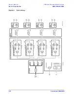
Figure 5-6 on page 5-22
is a simplified block diagram of the receiver functional group.
In this section the following assemblies are described:
•
A27, A28, A29, and A30 Receiver First Converters (Mixers)
•
A49 IF Multiplexer Board
•
A31, A32, A33, and A34 Receiver Modules
•
A6 SPAM Board (Analog Description)
•
A35 Receiver Motherboard
•
A16 Test Set Motherboard
A27, A28, A29, and A30 Receiver First Converters (Mixers)
The four receiver first converters (mixers) function identically and are completely interchangeable.
Each first converter receives the RF reference or test signal and mixes it with the 1st LO signal from the A20
LODA to create the 1st IF signal at a constant 8.333 MHz for bands 1–25 or 1.0416 MHz for band 0. This 1st
IF signal is sent to the LO reject/filter board.
A49 IF Multiplexer Board
In each of the four channels, a 3 MHz lowpass filter is switched into the signal path for band 0, to allow only
the 1st IF signal of 1.0416 MHz to pass but higher frequencies to be blocked. See
“IF Access Group (Option
H11)” on page 5-26
also.
A31, A32, A33, and A34 Receiver Modules
The four receiver modules function identically and are completely interchangeable.
The 8.333 MHz 1st IF signal is filtered and amplified. For bands 16-25, additional amplification is applied to
overcome conversion loss of the A27–A30 first converters in their third-order conversion mode.
A portion of the 8.333 MHz 1st IF signal is sent to a multiplexer on the A35 receiver motherboard, the output
of which is routed to the A11 phase lock board to complete the phase lock loop. The 8.333 MHz 1st IF signal
is also filtered, amplified, and routed to the 2nd converter.
The 2nd converter divides the 8.333 MHz signal into two paths and mixes each with a separate LO signal,
designated 2nd LO (a) and 2nd LO (b). Both of these 2nd LO signals are 1.000 MHz (for Band 0) or 8.29167
MHz (for Bands 1-25). The 2nd LO (b) signal is phase s90
relative to the 2nd LO (a) signal. These
two generated 2nd IF signals are a constant 41.667 kHz. These 2nd IF (a) and 2nd IF (b) signals are phase
shifted
45 degrees and +45 degrees, respectively. These signals are summed together and routed to the A6
signal processing and ADC module (SPAM) board.
Summary of Contents for E8362C
Page 11: ...Service Guide E8364 90038 1 1 1 Safety and Regulatory Information ...
Page 21: ...Service Guide E8364 90038 2 1 2 General Product Information ...
Page 33: ...Service Guide E8364 90038 3 1 3 Tests and Adjustments ...
Page 81: ...Service Guide E8364 90038 4 1 4 Troubleshooting ...
Page 137: ...Service Guide E8364 90038 5 1 5 Theory of Operation ...
Page 171: ...Service Guide E8364 90038 6 1 6 Replaceable Parts ...
Page 257: ...Service Guide E8364 90038 7 1 7 Repair and Replacement Procedures ...
Page 341: ...Service Guide E8364 90038 8 1 8 General Purpose Maintenance Procedures ...

