background image

– 4 –

DISASSEMBLY  INSTRUCTIONS

a

a

a

a

a

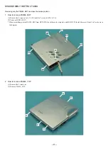
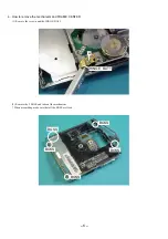
Removing only the PANEL, BOT can make the service position.

1. How to remove PANEL, BOT

(1) Remove the 5 screws a1-a5 (1.4-1.8) and the 2 screws b1,b2 (1.4-1.4).
(2) Take out PANEL, BOT.
* When assembling, put the PANEL, BOT from HP JACK side with care for strap hole and HOLD SW. Install the screws from 1 to 5 as shown in

the diagram.

2. How to remove PANEL, TOP

(1) Remove the 5 screws (a).
(2) Remove PANEL, TOP.

b2

a2

a1

a5

a4

a3

b1

Summary of Contents for AM-HX100

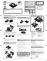
Page 1: ... T A MINIDISC PLAYER AM HX100 AHK S M Code No 09 018 446 0R2 R E V I S I O N BASIC MD MECHANISM BZG 8 A This Service Manual is the Revision Publishing and replaces Simple Manual of AM HX100 AHK S M Code No 09 015 446 0T2 ...

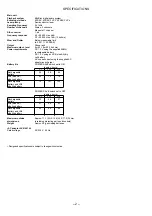
Page 2: ...sing an LR6 size AA dry cell battery AC house current using the supplied AC adaptor and charger Battery life POWER SAVE switch set to ON approx hours SP LP2 LP4 Rechargeable 29 38 45 battery LR6 size AA 40 72 75 alkaline battery Rechargeable 75 107 125 battery and LR6 alkaline battery POWER SAVE switch set to OFF approx hours SP LP2 LP4 Rechargeable 22 24 27 battery LR6 size AA 31 40 43 alkaline b...

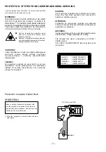
Page 3: ...paraten används på annat sätt än vad som specificeras i denna bruksanvising kan användaren utsättas för osynling laserstrålning som överskrider gränsen för laserklass 1 PROTECTION OF EYES FROM LASER BEAM DURING SERVICING CAUTION Use of controls or adjustments or performance of proce dures other than those specified herin may result in hazardous radiation exposure ATTENTION L utillisation de comman...

Page 4: ... 1 Remove the 5 screws a1 a5 1 4 1 8 and the 2 screws b1 b2 1 4 1 4 2 Take out PANEL BOT When assembling put the PANEL BOT from HP JACK side with care for strap hole and HOLD SW Install the screws from 1 to 5 as shown in the diagram 2 How to remove PANEL TOP 1 Remove the 5 screws a 2 Remove PANEL TOP b2 a2 a1 a5 a4 a3 b1 ...
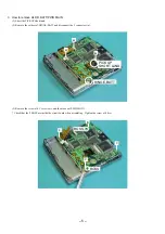
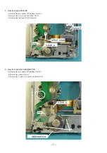
Page 5: ...LDR BATT PWB MAIN 1 Short the PICKUP Shortland 2 Remove the solders of HINGE BATT and disconnect the 3 connectors a 3 Remove the screw at b 3 screws at c and then take out PWB MAIN Check that the 2 BOSS are inside the circuit board when assembling Tighten the screw at b first ...

Page 6: ...BOSS BOSS BOSS 4 How to remove the mechanism and FRAME CENTER 1 Remove the screw a and the HINGE BATT 2 Remove the 5 BOSS and take out the mechanism When assembling make sure that all the BOSS are fixed HINGE BATT a ...

Page 7: ...e the screw a and the SPR P LEAD 3 Remove the shaft and PICK UP together a PW GEAR A SPR P LEAD PICK UP 6 How to remove the SLED MOTOR 1 Remove the poly washer PW and then GEAR A 2 Remove the solder fixed at a 3 Remove the 2 screws at b and the SLED MOTOR a b PW GEAR A SLED MOTOR ...

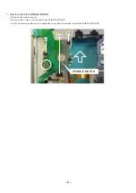
Page 8: ...PINDLE MOTOR 1 Remove the solder fixed at a 2 Remove the 3 screws at b1 b2 and b3 and SPINDLE MOTOR Follow the direction of the arrow to tighten the screws from b1 onwards to install the SPINDLE MOTOR b3 a b1 b2 SPINDLE MOTOR ...

Page 9: ...080 C CAP V 0 1 10 K B C212 87 A11 049 080 C CAP U 1 6 3 K B C213 87 A10 556 080 C CAP V 2200P 50 K B C216 87 A10 770 080 C CAP V 0 1 10 K B C300 87 A11 049 080 C CAP U 1 6 3 K B C301 87 A10 561 080 C CAP V 0 01 16 K B C302 87 A10 561 080 C CAP V 0 01 16 K B C303 87 A10 561 080 C CAP V 0 01 16 K B C304 87 A10 561 080 C CAP V 0 01 16 K B C305 87 A11 170 080 C CAP S 4 7 6 3 K B C306 87 A10 561 080 C...

Page 10: ...34 87 A00 760 080 C RES V 68K 1 16W F R335 87 A00 755 080 C RES V 6 8K 1 16W F R615 87 A01 014 080 C RES V 330K 1 16W F DESCRIPTION REF NO KANRI NO PART NO DESCRIPTION REF NO KANRI NO PART NO R616 87 A01 015 080 C RES V 560K 1 16W F R629 87 A01 013 080 C RES M F V 220K 1 16W D R630 87 A01 012 080 C RES M F V 34K 1 16W D R701 87 A91 879 080 C F BEAD BK1608TS102 R702 87 A91 879 080 C F BEAD BK1608TS...

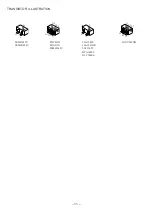
Page 11: ... 11 TRANSISTOR ILLUSTRATION B C E 2SA1588Y 2SA1832GR 2SC3265Y DTA144EE DTC144EE G D S SSM3J05FU SSM3K05FU FDC633N FDG311N SSM6J06FU D1 G D2 S D4 D3 HN1C03FUB E1 C2 B1 E2 C1 B2 ...

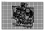
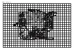
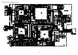
Page 12: ...WIRING 1 MAIN 1 2 1 2 3 4 5 6 7 8 9 10 11 12 13 14 15 16 17 18 19 20 21 22 23 24 25 26 27 28 29 30 31 32 12 A B C D E F G H I J K L M N O P Q R S T U ...

Page 13: ...WIRING 1 MAIN 2 2 32 31 30 29 28 27 26 25 24 23 22 21 20 19 18 17 16 15 14 13 12 11 10 9 8 7 6 5 4 3 2 1 13 A B C D E F G H I J K L M N O P Q R S T U ...

Page 14: ... 14 SCHEMATIC DIAGRAM MAIN FLEX JACK ...

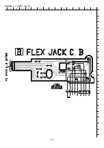
Page 15: ...WIRING 2 FLEX JACK 15 14 13 12 11 10 9 8 7 6 5 4 3 2 1 A B C D E F G H I J K L M N O P Q R S T U 15 ...

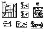
Page 16: ... 16 IC BLOCK DIAGRAM ...

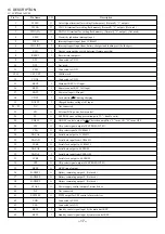
Page 17: ...D input 20 22 NC Not connected 23 PD O External DAC power down control 24 PE O EEPROM error writing prevention port L disable write 25 VDSW O ON OFF control output for V detection amplifier L turns ON H turns OFF 26 CE3 O Chip select signal output of EEPROM IC303 27 CEQ O Chip select signal of LC896431 28 DATA0 O Serial data output to LC896431 29 DATAD I Serial data input from LC896431 30 SCK0 O S...

Page 18: ...ntrol output 62 NIHM O O Battery charge output 63 BSTSW O Head phone amplifier bus boost ON OFF switch BST on with H 64 BST2 O DSL 3 STEP switch output 65 BST3 O DSL 3 STEP switch output 66 HP LINE O Head phone amplifier line switch output 67 LED1 O Operation LED control signal output LED on with H 68 VSS3 Connected to GND 69 VDD3 Connected to VDD 70 CHG 1 O Battery charge stand LED control output...

Page 19: ...al input 19 FE I Focus error signal input terminal 20 VC I Intermediate electric potential input terminal 21 AVDD1 Power supply terminal for digital servo 22 DSW1 O Disc mode switch output 23 DSW0 O Disc mode switch output 24 SGC O AGC control signal output terminal 25 AOFFSET O ABCD offset control signal output terminal 26 FOFFSET O Focus offset control signal output terminal 27 TOFFSET O Trackin...

Page 20: ...al 64 BEMFV I Sled control signal input terminal 65 BEMFW 66 FOPWMF O Focus PWM output terminal 67 FOPWMR O Focus PWM output terminal 68 TRPWMF O Tracking PWM output terminal 69 TRPWMR O Tracking PWM output terminal 70 FG I Speed pulse input terminal 71 VP O LCV servo lock recognition output 72 FOK O Focus OK signal output terminal 73 FAST O FAST signal output terminal Not used 74 CL I Data transf...

Page 21: ...EST1 I Test input terminal Connected to VCC 102 NC I O Not connected 103 MAD5 O Address output terminal to DRAM 104 MAD4 O Address output signal to DRAM 105 TEST3 I Test input terminal Connected to VCC 106 VSS Ground terminal 107 VCC2 Power supply terminal 108 SMON3 O Monitor signal output 109 SMON2 O Monitor signal output 110 MAD3 O Address output terminal to DRAM 111 MAD2 O Address output termin...

Page 22: ...nal 19 AOFF I Offset adjustment pin of ABCD signal 20 SGC I VCA gain control pin 21 DSW0 I Disc mode setting pin Hi Disc with low reflectance Lo Disc with high reflectance Laser OFF when DSWO and DSW1 are Lo 22 DSW1 I Disc mode setting pin Hi Track in pit line Lo Track in group Laser OFF when DSWO and DSW1 are Lo 23 VR By pass capacitor connection pin for 1 2 VCC 24 VC O 1 2 VCC output pin 25 FE O...

Page 23: ... GLHSW 6dB down with Hi 42 RAGCSW RFAGC ON OFF switch pin RFAGC Lo AGC on RFAGC Hi AGC off Connected to VEE 43 WOO O Wobble signal output pin 44 WOI I Wobble signal input pin 45 SETR I Band pass filter setting pin 46 CAD Capacitor connection pin of wobble signal for DC cut 47 BWCT I Band pass filter switch pin of wobble signal 48 SLEEP I Sleep mode SLEEP Hi Power ON SLEEP Lo Power OFF ...

Page 24: ...scillation frequency control terminal 22 RMAX VCO highest oscillation frequency setup terminal 23 RMIN VCO lowest oscillation frequency setup terminal 24 VCTL NC Speed control terminal Not used 25 VCREF NC Speed control standard voltage terminal Not used 27 SPPWMF I PWM signal input terminal 28 GND GND terminal of bipolar circuit part 30 BEMFW 31 BEMFV O Sled motor comparator output terminal 32 BE...

Page 25: ... 51 CPC1 52 CPC2 Connecting terminal to 2nd phase capacitor of charge pump 53 CPO Connecting terminal to last phase capacitor of charge pump 54 RF1 I Spindle motor electric current detection terminal Connected to GND 55 59 VS Spindle motor drive power supply terminal Connected to VM 56 SPWOUT 57 SPVOUT O Spindle motor power supply output terminal 58 SPUOUT 60 RF2 I Spindle motor electric current d...

Page 26: ...f playback operations These modes may be selected using VOL keys while they can be started or stopped by pressing PLAY key If a Test Mode is selected a data will be displayed in XXXX The values displayed in XXXX are just IC internal data and their numerical values are of no significance except for that of No 0 13 If any abnormalities were detected during the operation it displays Failed Example of...

Page 27: ...g Sled Operation Sled operation can be checked between Mode No 0 5 12 Press F SKIP to shift the pick up towards the external circumference Press B SKIP to shift the pick up towards the internal circumference 3 Checking Switch Operation OPEN CLOSE SW and HOLD SW on a disc holder can be checked on LCD of the remote controller Light up when the disc holder is closed Alarm mark will light up when HOLD...

Page 28: ...DC POWER SUPPLY Oscilloscope 2 Note If a disc had any stains or scars on the adjustment may not be completed Always place the main unit with its cassette cover upward for adjustment Do not make any manual adjustment If the adjustment is incomplete it displays NO ADJ during normal operation 3 Prohibitions Do not press DSL key of the remote controller If it was pressed the mode will change to factor...

Page 29: ...he top panel is upward LCD of the remote controller will be displayed AUTO ADJ H first then COMPLETE Press PLAY STOP key again to display IDLE If it displayed Failed during adjustment it means that some abnormalities are detected and the operation is terminated 5 GRV disc SONY MDW 74 Insert the disc and press PLAY key Check the facing direction of the set LCD of the remote controller will be displ...

Page 30: ... 30 MECHANICAL EXPLODED VIEW 1 1 BZG 8A PWB JACK B D A F B B E E C D A A A 12 15 1 2 5 4 19 6 7 8 9 10 21 20 11 SH PANEL BOT 13 14 16 17 b b a a 18 3 ...

Page 31: ...EL BOT AHK1S 18 8B HM4 020 010 PANEL BOT L AHK1L 19 8B HM4 010 010 PLATE DECO AHK1S 19 8B HM4 012 010 PLATE DECO C AHK1L 20 8B ZG8 228 010 HLDR ASSY CTRG R 21 8B HM4 210 110 SPR T OPEN A 87 HM1 243 010 S SCREW 1 4 1 4CRNL B 8A HM5 221 010 S SCREW 1 4 1 8 CR N C 8A HM3 233 010 S SCREW 1 4 3 5 N D 8A HM3 222 010 S SCREW 1 4 3 0 CR E 87 078 186 010 SCRW SR 1 4 1 8 CR L F 87 B10 152 010 W P 0 83 2 0 0...

Page 32: ...10 GEAR A 4 M8 ZZS 294 000 ZZS 2 C 5 8A ZGF 209 010 GEAR B 6 8Z ZG5 217 010 BRG 1 1 2 2 7 8A ZGF 210 010 SHAFT LEAD 8 8A ZGF 212 010 SPR P LEAD 9 87 A91 718 110 PICKUP KMS 330A 10 8Z ZG5 219 010 SPR P RACK 2 11 8B ZG8 238 010 SPR E LOCK 12 8B ZG8 237 010 SPR E EJECT A 88 ZG6 224 010 S SCREW VBT 1 4 3 B 8A ZGF 220 010 S SCREW V 1 4 1 2 C 87 067 569 010 POLY WASHER 0 83 2 5 0 25 D 8Z ZG5 223 010 S S...

Page 33: ...7 B30 221 010 CASE BATTERY 4 87 B30 450 010 HEADPHONE HP M056A S 5 8B HM4 953 010 BOX BAT ASSY BHM 4 AHK1S 5 8B HM4 955 010 BOX BAT ASSY BHM 4 L AHK1L 6 8B HM4 952 010 RC UNIT RC HX100 7 8A HM6 954 110 CLIP RC CL33 8 8B HM4 954 010 BAG CARRING BHM 4 9 87 B30 144 010 AC ADAPTOR AC D401K NC 10 8B HM4 957 010 CHARGER RB M05 HX100 EX ...

Page 34: ...2 11 IKENOHATA 1 CHOME TAITO KU TOKYO 110 JAPAN TEL 03 3827 3111 Printed in Singapore 2000068 921338 ...

Page 35: ...SERVICE MANUAL DATA AM HX100 AHK SIMPLE S M Code No 09 015 446 0T2 Replace this Service manual with Revision Publishing when it is issued MINIDISC PLAYER BASIC MD MECHANISM BZG 8 A ...

Page 36: ...80 0E C CAP V 100P 50 J CH AHK1L AM HX100 O AUDIO C 0705 87 A10 543 080 0E C CAP V 100P 50 J CH AHK1S AM HX100 O AUDIO C 0706 87 A11 049 080 0E C CAP U 1 6 3 K B AHK1L AM HX100 O AUDIO C 0706 87 A11 049 080 0E C CAP U 1 6 3 K B AHK1S AM HX100 O AUDIO C 0707 87 A11 170 080 1A C CAP S 4 7 6 3 K B AHK1L AM HX100 O AUDIO C 0707 87 A11 170 080 1A C CAP S 4 7 6 3 K B AHK1S AM HX100 O AUDIO C 0708 87 A11...

Page 37: ...3 080 0E C RES V 12K 1 16W J AHK1S AM HX100 X AUDIO R 0704 88 104 123 080 0E C RES V 12K 1 16W J AHK1L AM HX100 X AUDIO R 0704 88 104 123 080 0E C RES V 12K 1 16W J AHK1S AM HX100 X AUDIO R 0705 88 104 104 080 0E C RES V 100K 1 16W J AHK1L AM HX100 X AUDIO R 0705 88 104 104 080 0E C RES V 100K 1 16W J AHK1S AM HX100 X AUDIO R 0706 88 104 223 080 0E C RES V 22K 1 16W J AHK1L AM HX100 X AUDIO R 0706...

Page 38: ...K B AHK1S AM HX100 O DRIVER C 0404 87 A10 561 080 0E C CAP V 0 01 16 K B AHK1L AM HX100 O DRIVER C 0404 87 A10 561 080 0E C CAP V 0 01 16 K B AHK1S AM HX100 O DRIVER C 0405 87 A11 049 080 0E C CAP U 1 6 3 K B AHK1L AM HX100 O DRIVER C 0405 87 A11 049 080 0E C CAP U 1 6 3 K B AHK1S AM HX100 O DRIVER C 0406 87 A10 353 080 0E C CAP U 0 22 10 K B AHK1L AM HX100 O DRIVER C 0406 87 A10 353 080 0E C CAP ...

Page 39: ... S DSP IC 0200 87 A21 835 010 2C C IC LC896431 AHK1S AM HX100 S DSP IC 0201 87 A21 526 010 2P C IC GM71VLS17403CTL 1 AHK1L AM HX100 S DSP IC 0201 87 A21 526 010 2P C IC GM71VLS17403CTL 1 AHK1S AM HX100 O DSP L 0200 87 003 245 080 0E C COIL 2125 22UH K MLF2012 AHK1L AM HX100 O DSP L 0200 87 003 245 080 0E C COIL 2125 22UH K MLF2012 AHK1S AM HX100 X DSP R 0200 88 104 103 080 0E C RES V 10K 1 16W J A...

Page 40: ...K1L AM HX100 X OTHERS 8A HM5 223 010 0E CUSH R JACK AHK1S AM HX100 X OTHERS 8A HM5 224 010 0E SH PROT JACK AHK1L AM HX100 X OTHERS 8A HM5 224 010 0E SH PROT JACK AHK1S AM HX100 O OTHERS 8B HM4 201 010 FRAME ASSY R AHK1L AM HX100 O OTHERS 8B HM4 201 010 FRAME ASSY R AHK1S AM HX100 X OTHERS 8B HM4 202 010 FRAME R AHK1L AM HX100 X OTHERS 8B HM4 202 010 FRAME R AHK1S AM HX100 X OTHERS 8B HM4 203 010 A...

Page 41: ...55 010 CTN PRINTED AHK1S AHK1S AM HX100 X PACKING 8B HM4 856 010 CTN OUTER AHK1 S AHK1S AM HX100 X PACKING 8B HM4 857 010 CUSHION AHK1S AHK1L AM HX100 X PACKING 8B HM4 857 010 CUSHION AHK1S AHK1S AM HX100 X PACKING 8B HM4 858 010 CTN OUTER AHK1 L AHK1L AM HX100 X PLATE 87 057 961 010 0E LBL CAUTION TRIANGLE AHK1L AM HX100 X PLATE 87 057 961 010 0E LBL CAUTION TRIANGLE AHK1S AM HX100 X PLATE 87 B40...

Page 42: ... AHK1L AM HX100 O POWER SUPPLY PR 0600 87 A91 769 080 1A C PROTECTOR 0 75A ERY32SB075 AHK1S AM HX100 O POWER SUPPLY PR 0601 87 A91 769 080 1A C PROTECTOR 0 75A ERY32SB075 AHK1L AM HX100 O POWER SUPPLY PR 0601 87 A91 769 080 1A C PROTECTOR 0 75A ERY32SB075 AHK1S AM HX100 S POWER SUPPLY Q 0600 87 A30 604 080 1A C FET FDG311N AHK1L AM HX100 S POWER SUPPLY Q 0600 87 A30 604 080 1A C FET FDG311N AHK1S ...

Page 43: ...0 0E C RES V 47K 1 16W J AHK1S AM HX100 X POWER SUPPLY R 0623 88 104 103 080 0E C RES V 10K 1 16W J AHK1L AM HX100 X POWER SUPPLY R 0623 88 104 103 080 0E C RES V 10K 1 16W J AHK1S AM HX100 X POWER SUPPLY R 0624 88 104 473 080 0E C RES V 47K 1 16W J AHK1L AM HX100 X POWER SUPPLY R 0624 88 104 473 080 0E C RES V 47K 1 16W J AHK1S AM HX100 X POWER SUPPLY R 0625 88 104 474 080 0E C RES V 470K 1 16W J...

Page 44: ...100 O RF C 0125 87 A10 770 080 0E C CAP V 0 1 10 K B AHK1L AM HX100 O RF C 0125 87 A10 770 080 0E C CAP V 0 1 10 K B AHK1S AM HX100 O RF C 0126 87 A11 058 080 0E C CAP U 0 22 10 K B AHK1L AM HX100 O RF C 0126 87 A11 058 080 0E C CAP U 0 22 10 K B AHK1S AM HX100 O RF C 0127 87 A11 049 080 0E C CAP U 1 6 3 K B AHK1L AM HX100 O RF C 0127 87 A11 049 080 0E C CAP U 1 6 3 K B AHK1S AM HX100 O RF CN 0100...

Page 45: ...MPER V AHK1S AM HX100 X RF R 0132 88 104 103 080 0E C RES V 10K 1 16W J AHK1L AM HX100 X RF R 0132 88 104 103 080 0E C RES V 10K 1 16W J AHK1S AM HX100 X RF R 0134 88 104 000 080 0E C JUMPER V AHK1L AM HX100 X RF R 0134 88 104 000 080 0E C JUMPER V AHK1S AM HX100 X RF R 0135 88 104 823 080 0E C RES V 82K 1 16W J AHK1L AM HX100 X RF R 0135 88 104 823 080 0E C RES V 82K 1 16W J AHK1S AM HX100 X RF R...

Page 46: ...HX100 O SYSTEM CONTROL R 0306 87 A00 759 080 C RES V 27K 1 16W F AHK1S AM HX100 X SYSTEM CONTROL R 0307 88 104 224 080 0E C RES V 220K 1 16W J AHK1L AM HX100 X SYSTEM CONTROL R 0307 88 104 224 080 0E C RES V 220K 1 16W J AHK1S AM HX100 X SYSTEM CONTROL R 0308 88 104 104 080 0E C RES V 100K 1 16W J AHK1L AM HX100 X SYSTEM CONTROL R 0308 88 104 104 080 0E C RES V 100K 1 16W J AHK1S AM HX100 X SYSTEM...

Page 47: ...SH 2 1 1 SPVE3 8 AHK1S AM HX100 O SYSTEM CONTROL S 0301 87 A92 166 080 1A C SW SL 1 1 2 HSW4512 31 AHK1L AM HX100 O SYSTEM CONTROL S 0301 87 A92 166 080 1A C SW SL 1 1 2 HSW4512 31 AHK1S AM HX100 O SYSTEM CONTROL S 0302 87 A91 979 080 0E C SW TACT SOT 152HST AHK1L AM HX100 O SYSTEM CONTROL S 0302 87 A91 979 080 0E C SW TACT SOT 152HST AHK1S AM HX100 O SYSTEM CONTROL S 0303 87 A91 979 080 0E C SW T...

Page 48: ... 14 SCHEMATIC DIAGRAM 1 MAIN ...

Page 49: ...2 11 IKENOHATA 1 CHOME TAITO KU TOKYO 110 JAPAN TEL 03 3827 3111 Printed in Singapore 9820543 ...

Reviews: