28
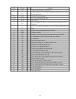
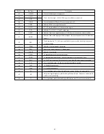
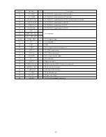
IC DESCRIPTION
1
2
3
4
5
6
7
8
9
10
11
12
13
14
15
16
17
18
19
20
21
22
23
24
25
26
27
28
29
30, 31
32, 33
34
35
FIN2
FIN1
E
F
TB
TE–
TE
TESI
SCI
TH
TA
TD–
TD
JP
TO
FD
FD–
FA
FA–
FE
FE–
AGND
SP
SPI
SPG
SP–
SPD
SLEQ
SLD
SL–, SL+
JP–, JP+
TGL
TOFF
I
I
I
I
I
I
O
I
I
I
O
I
I
I
O
O
I
I
I
O
I
—
—
O
I
I
O
I
O
I
I
I
I
Pin to which external pickup photo diode is connected. RF signal is created by adding
with the FIN1 pin signal. FE signal is created by subtracting from the FIN1 pin signal.
Pin to which external pickup photo diode is connected.
Pin to which external pickup photo diode is connected. TE signal is created by
subtracting from the F pin signal.
Pin to which external pickup photo diode is connected.
DC component of the TE signal is input.
Pin to which external resistor setting the TE signal gain is connected between the TE pin.
TE signal output pin.
TES “Track Error Sense” comparator input pin. TE signal is passed through a band-
pass filter then input.
Shock detection signal input pin.
Tracking gain time constant setting pin.
TA amplifier output pin.
Pin to which external tracking phase compensation constants are connected between
the TD and VR pins.
Tracking phase compensation setting pin.
Tracking jump signal (kick pulse) amplitude setting pin.
Tracking control signal output pin.
Focusing control signal output pin.
Pin to which external focusing phase compensation constants are connected between
the FD and FA pins.
Pin to which external focusing phase compensation constants are connected between
the FD– and FA– pins.
Pin to which external focusing phase compensation constants are connected between
the FA and FE pins.
FE signal output pin.
Pin to which external FE signal gain setting resistor is connected between the FE pin.
Analog signal GND.
No connection.
Single ended output of the CV+ and CV– pin input signal.
Pin to which external spindle gain setting resistor in 12 cm mode is connected.
Pin to which external spindle phase compensation constants are connected together
with SPD pin.
Spindle control signal output pin.
Pin to which external sled phase compensation constants are connected.
Sled control signal output pin.
Sled advance signal input pin from microprocessor.
Tracking jump signal input pin from DSP.
Tracking gain control signal input from DSP. Low gain when TGL = H.
Tracking off control signal input pin from DSP. Off when TOFF = H.
IC, LA9241ML
Pin No.
Pin Name
I/O
Description
Summary of Contents for CSD-EL300 EZ(S)
Page 8: ...8 LCD DISPLAY LCD AIW4213...
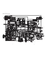
Page 9: ...10 9 SCHEMATIC DIAGRAM 1 MAIN...
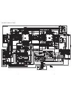
Page 10: ...12 11 SCHEMATIC DIAGRAM 2 CD MAIN...
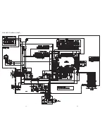
Page 11: ...1 2 3 4 5 6 7 8 9 10 11 12 13 14 A B C D E F G H I J K 14 13 WIRING 1 MAIN CD MAIN...
Page 14: ...20 19 SCHEMATIC DIAGRAM 4 FRONT SOL2...
Page 15: ...1 2 3 4 5 6 7 8 9 10 11 12 13 14 A B C D E F G H I J K 22 21 WIRING 4 FRONT...
Page 17: ...25 IC BLOCK DIAGRAM IC TA2149N IC LC72121M...
Page 19: ...27 IC LA6541D...
Page 34: ...2 11 IKENOHATA 1 CHOME TAITO KU TOKYO 110 JAPAN TEL 03 3827 3111 737004 Printed in Singapore...


