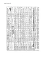
– 35 –
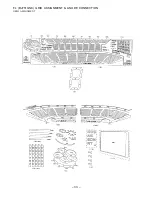
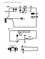
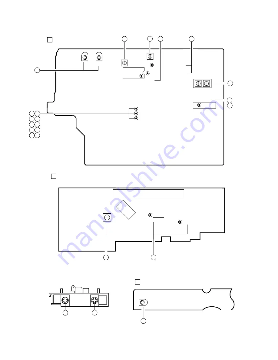
ADJUSTMENT <TUNER / DECK / MICON>
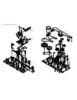
MAIN C.B
A
L951
SFR351
SFR352
L801
TP2 (CLK)
TP3 (DC BALANCE)
GND
TP9 (RCH)
TP8 (LCH)
10
2
L802
7
4
TP1 (VT)
(3/3) (1/3)
FFE831
(O-KSCAN)
14
MICON C.B
B
FL101
L101
SFR1
8
TP4 (DC BALANCE)
6
1
3
5
6
7
8
9
11
12
13
7
12
14
IC801
4
IC101
TP7
D-GND
DECK C.B
K
DECK–1 P HEAD
DECK–2 R/P/E HEAD
REV
FWD
9
9
Summary of Contents for CX-ZL900
Page 13: ...SCHEMATIC DIAGRAM 1 MAIN 1 3 AMP SECTION VM 13 ...
Page 14: ...SCHEMATIC DIAGRAM 2 MAIN 2 3 DECK SECTION HEAD 1 HEAD 2 14 ...
Page 15: ...SCHEMATIC DIAGRAM 3 MAIN 3 3 TUNER SECTION 15 ...
Page 17: ...SCHEMATIC DIAGRAM 4 MICON DECK 17 ...
Page 20: ...SCHEMATIC DIAGRAM 5 CNTL MIC KEY CD DK1 LED DK2 LED 20 ...
Page 22: ...SCHEMATIC DIAGRAM 6 AMP 1F 22 ...
Page 24: ...SCHEMATIC DIAGRAM 7 PT 24 ...
Page 28: ... 28 IC BLOCK DIAGRAM ...
Page 29: ... 29 ...
Page 30: ... 30 ...
Page 31: ... 31 ...
Page 32: ... 32 ...
Page 33: ... 33 FL BJ751GNK GRID ASSIGNMENT ANODE CONNECTION GRID ASSIGNMENT ...
Page 34: ... 34 ANODE CONNECTION ...