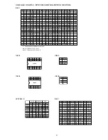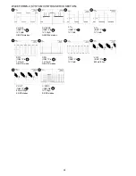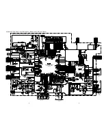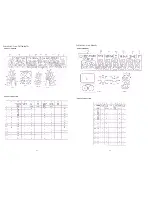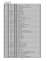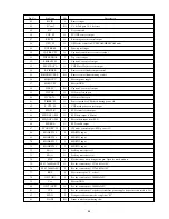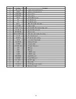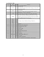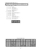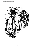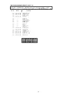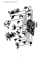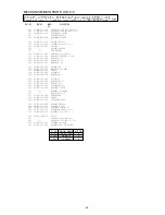
Pin No.
Pin Name
I/O
Description
57
IC,
µ
PD16311GC-AB6
I
O
I
–
I
I
I
I
I
–
O
O
–
–
O
–
O
O
O
–
–
1 ~ 4
5
6
7
8
9
10
11
12
13
14
15 ~ 26
27 ~ 32
33
34
35
36 ~ 44
45
46 ~ 48
49
50
51
52
SHTL1 ~SHTL4
DATA OUT
DATA IN
IC
CLOCK
FLD ENV
KEY1
KEY2
KEY3
KEY4
Vdd
P1 ~ P12
P13 ~ P16
Vdd
Vcc
NC
G1 ~ G9
Vdd
NC
OTPB LED 'H'
NC
Vss
OSC
4-bit general-purpose input pins
Serial data output.
Lower bits are first output synchronized with the trailing edge of shift clock. (The
output is Nch open drain.)
Serial data input.
Lower bits are first input synchronized with the leading edge of shift clock.
Must always be set to open (set to VDD voltage)
Serial data is input at the leading edge, and data is output at the trailing edge.
The leading or trailing edge initializes the serial I/F to stand by for receiving a
command. The data input after the STB trailing edge is processed as a command.
When command or data is being processed, the processing is interrupted and the serial
I/F is initialized. When STB is “H”, CLK is ignored.
Data input to these pins is latched in the final stage of display cycle.
5 V
±
10%
Exclusively used for segment outputs
Segment/grid outputs swicthable
5 V
±
10%
Vdd – 35 V MAX.
Not connected
Exclusively used for grid outputs
5 V
±
10%
Not connected
OTPB LED Driver (OTPB mode “H”)
Not connected
Connected to system ground
For the connection of resistors that determine the oscillation frequency

