– 42 –
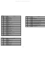
I/O
Description
Pin No.
Pin Name
1,21~22,27,28
TP (NC)
–
Test Pin.
2, 19, 26, 32
NC
–
Not connected
3
D CTR OUT1 (NC)
O
Digital control output1.
4
D CTR OUT0(NC)
O
Digital control output0.
5
ADR SEL
I
I2C Bus adress select.
6
STANDBYQ
I
Standby (Low active).
7
I2C CL
I/O
I2C clock.
8
I2C DA
I/O
I2C data.
9~15
TP (NC)
–
Test pin.
16
DVSUP
–
DIGITAL POWER 5V.
17
DVSS
–
DIGITAL GROUND.
18
TP (NC)
I
Test pin.
20
RESETQ
I
Power-on reset.
23
VREF2
–
Reference ground 2 high voltage part.
24
DACM R
O
Speaker out, right.
25
DACM L
O
Speaker out, left.
29
VREF1
–
Reference ground 1 high voltage part.
30
SC1 OUT R
O
Serial output 1 right.
31
SC1 OUT L
O
Serial output 1 left.
33
AHVSUP
–
Analog power suppy 8.0 V.
34
CAPL M
–
Volume capacitor MAIN.
35
AHVSS
–
Analog ground.
36
AGNDC
–
Analog reference voltage high voltage part.
37 ~ 40
NC
–
Not conncted.
41
SC1 IN L
I
Scart input 1 in, left.
42
SC1 IN R
I
Scart input 1 in, right.
43
VREFTOP
–
Reference voltage IF A/D converter.
44
MONO IN
I
Mono input.
IC, MSP3417D
I/O
Description
Pin No.
Pin Name
1
IN8
I
MESECAM/PAL detection input.
2, 11, 12
NC
–
Not use.
3
SPDATA
O
Serial data signal.
4 ~ 7
IN4 ~ 1
I
Shuttle switch signal input 4 ~ 1.
8
GND
–
GND.
9
STRB
I
TC4021 chip select signal.
10
CLK
I
Serial clock signal.
13, 14
IN5, 6
I
Jog switch signal input 1, 2.
15
IN7
I
Power monitoring input.
16
VCC
–
Power 5V.
IC, TC4021BF
I/O
Description
Pin No.
Pin Name
1
VSS
–
Ground (0V).
2
SCL
I
Serial clock input of I
2
C Bus.
3
SDA
I
Serial data input of I
2
C Bus.
4.
CSO
I
Chip select input determining the I
2
C-Bus addresses: 20H/21H, (low) 22H/23H, (high).
5
VCS
O
Video Composite Sync output from sync slicer used for PLL based clock generation.
6
DAV
O
Data available output active low, when VPS data is received.
7
EHB
O
Output signaling the presence of the first field active high.
8
TI
I
Test input; activates test mode when pulled high. Connect to ground for operating mode.
9
PD1
O
Phase detector/charge pump output of data PLL (DAPLL).
10
PD2
I/O
Connector of the loop filter for the SYSPLL.
11
VCO
I
Input to the voltage controlled oscillator #1 of the DAPLL.
12
IREF
I
Reference current input for the on-chip analog circuit.
13
CBVS
I
Composite video signal input.
14
VDD
–
Positive supply voltage (+5V nom).
IC, SDA5650P–DIP–14
All manuals and user guides at all-guides.com
Summary of Contents for HV-FX8700
Page 3: ...3 All manuals and user guides at all guides com...
Page 12: ...12 C WIRE HARNESS DIAGRAM All manuals and user guides at all guides com...
Page 13: ...BLOCK DIAGRAM 1 SYSCON SERVO 13 All manuals and user guides at all guides com...
Page 14: ...BLOCK DIAGRAM 2 VIDEO 14 All manuals and user guides at all guides com...
Page 16: ...16 BLOCK DIAGRAM 4 TUNER All manuals and user guides at all guides com a l l g u i d e s c o m...
Page 17: ...17 BLOCK DIAGRAM 5 MPX All manuals and user guides at all guides com...
Page 18: ...BLOCK DIAGRAM 6 CANAL 18 SWITCH Q610 WIDE All manuals and user guides at all guides com...
Page 19: ...19 BLOCK DIAGRAM 7 POWER PS All manuals and user guides at all guides com...
Page 22: ...22 SCHEMATIC DIAGRAM 2 MAIN 2 4 VIDEO SECTION All manuals and user guides at all guides com...
Page 23: ...23 SCHEMATIC DIAGRAM 3 MAIN 3 4 HIFI SECTION All manuals and user guides at all guides com...
Page 25: ...25 SCHEMATIC DIAGRAM 4 FR1 FR2 All manuals and user guides at all guides com...
Page 27: ...27 SCHEMATIC DIAGRAM 6 REAR 2 2 CANAL SECTION All manuals and user guides at all guides com...
Page 29: ...29 SCHEMATIC DIAGRAM 7 TUNER All manuals and user guides at all guides com...
Page 30: ...30 SCHEMATIC DIAGRAM 8 MAIN 4 4 POWER SECTION All manuals and user guides at all guides com...
Page 32: ...32 SCHEMATIC DIAGRAM 10 MPX All manuals and user guides at all guides com...
Page 38: ...38 IC BLOCK DIAGRAM All manuals and user guides at all guides com...

