background image

-23-

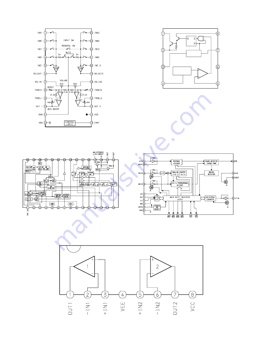
IC BLOCK DIAGRAM-1/1

IC, M62495AFP

IC, LA1837NL

IC, LC72131D

IC, BA4560N

Switch collector

Driver

Peak currect 
detection

Power supply

Comparator input

Switch emitter

External capacitance

for oscillation

Ground

1.17V 

REF. VOL

OSC

IC, M5291FP

Summary of Contents for LCX-K277

Page 1: ...SERVICE MANUAL D A T A BASIC TAPE MECHANISM TN 21ZSC 2003 BASIC CD MECHANISM DA 11T3C COMPACT DISC STEREO SYSTEM LCX K277 S M Code No 09 007 347 4N2 HC S MODEL CODE 86HR8 0117 B ...

Page 2: ... 2 SPECIFICATIONS Design and specifications are subject to change without notice ...

Page 3: ...han those specified herein may result in hazardous radiation exposure ATTENTION L utilisation de commandes réglages ou procédures autres que ceux spécifiés peut entraîner une dangereuse exposition aux radiations ADVARSEL Usynlig laserståling ved åbning når sikkerhedsafbrydereer ude af funktion Undgå udsættelse for stråling This Compact Disc player is classified as a CLASS 1 LASER product The CLASS...

Page 4: ...After the connection remove solder shown in the right figure Body or clothes electrostatic potential could ruin laser diode in the optical block Be sure ground body and workbench and use care the clothes do not touch the diode Solder PICK UP Assy P W B ...

Page 5: ...LECT 220 10V C204 87 010 197 080 CAP CHIP 0 01 DM C213 87 016 669 080 C CAP S 0 1 25 K B C214 87 016 669 080 C CAP S 0 1 25 K B C223 87 A11 123 080 CAP TC U 1800P C224 87 A11 123 080 CAP TC U 1800P C225 87 010 401 080 CAP ELECT 1 50V C226 87 010 401 080 CAP ELECT 1 50V C227 87 018 208 080 CAP 0 047 50F C228 87 018 208 080 CAP 0 047 50F C229 87 018 132 080 CAP CER 2200P 16V C230 87 018 132 080 CAP ...

Page 6: ...OR 0 1 25 C961 87 012 170 080 C CAP U 8P 50 CH C963 87 010 196 080 CHIP CAPACITOR 0 1 25 CF801 87 008 261 010 FILTER SFE10 7MA5 A CF802 87 008 261 010 FILTER SFE10 7MA5 A CN101 87 049 919 010 CONN 3P EH V WHT CN201 87 099 719 010 CONN 30P TYK B X CN203 87 A60 060 010 CONN 07P V 9604S 07C CN301 87 A60 627 010 CONN 10P V 2MM JMT FB701 87 008 372 080 FILTER EMI BL OIRNI FB702 87 008 372 080 FILTER EM...

Page 7: ...CHIP 0 01 DM C513 87 010 197 080 CAP CHIP 0 01 DM C514 87 010 197 080 CAP CHIP 0 01 DM C518 87 010 322 080 C CAP S 100P 50 CH C519 87 012 145 080 CAP CHIP S 270P CH C520 87 012 157 080 C CAP S 330P 50 CH C521 87 012 154 080 C CAP S 150P 50 CH C522 87 010 371 080 CAP ELECT 470 6 3V C523 87 010 197 080 CAP CHIP 0 01 DM C524 87 010 197 080 CAP CHIP 0 01 DM C525 87 010 197 080 CAP CHIP 0 01 DM C526 87...

Page 8: ... TACT KSH0611BT S902 87 A91 024 180 SW TACT KSH0611BT S904 87 A91 024 180 SW TACT KSH0611BT S905 87 A91 024 180 SW TACT KSH0611BT S906 87 A91 024 180 SW TACT KSH0611BT S907 87 A91 024 180 SW TACT KSH0611BT S908 87 A91 024 180 SW TACT KSH0611BT S909 87 A91 024 180 SW TACT KSH0611BT S910 87 A91 024 180 SW TACT KSH0611BT S911 87 A91 024 180 SW TACT KSH0611BT S913 87 A91 024 180 SW TACT KSH0611BT S915...

Page 9: ... 9 10 11 12 13 14 15 16 17 18 19 20 21 22 23 24 A B C D E F G H I J K L M N O P Q R S T U 1 2 3 4 5 6 7 8 9 25 26 27 28 29 30 31 32 WIRING 1 5 MAIN C965 C810 C743 C741 C742 C700 FB703 FB702 1 2 3 4 5 6 ...

Page 10: ... 10 SCHEMATIC DIAGRAM 1 5 MAIN1 2 TAPE DECK TN 21ZSC 2003 TO VCD C B CN405 TO VCD C B 1 2 12V FB701 S101 AC VOLTAGE FB704 FB703 FB702 FB705 IC102 NJM7812FA 1800p 1800p GND L202 JW J203 JW ...

Page 11: ... 11 SCHEMATIC DIAGRAM 2 5 MAIN2 2 TUNER C700 0 1 12V ...

Page 12: ... 19 20 21 22 23 24 A B C D E F G H I J K L M N O P Q R S T U 1 2 3 4 5 6 7 8 9 25 26 27 28 29 30 31 32 WIRING 2 5 MICON KEY LED 30 31 1 100 80 81 50 51 TO VCD C B CN403 S920 VOLUME MULTI JOG CD PBC SELECT CLEAR RETURN PREVIOUS NEXT ...

Page 13: ...ICON XBUSY COMMAND STATUS XBUSY COMMAND STATUS SCK SCK N C N C TO VCD C B CN403 XBUSY COMMAND STATUS I STATUS SCK I O XBUSY O COMMAND O SCK IC601 LC877248A 5R97 DESTINATION CD PBC PRESET SELECT CLEAR RETURN UP NEXT DOWN PREVIOUS ...

Page 14: ... 14 WIRING 3 5 VCD COMPONENT SIDE 18 19 20 21 22 23 24 25 26 27 28 29 30 31 32 A B C D E F G H I J K L M N O P Q R S T U 17 16 15 14 13 12 11 10 9 8 7 6 5 4 3 2 1 ...

Page 15: ... 15 WIRING 4 5 VCD CONDUCTOR SIDE 15 14 13 12 11 10 9 8 7 6 5 4 3 2 1 A B C D E F G H I J K L M N O P Q R S T U 16 17 18 19 20 21 22 23 24 25 26 27 28 29 30 31 32 C605 J501 CN203 PIN3 CN405 CN101 CN602 ...

Page 16: ... 16 SCHEMATIC DIAGRAM 4 5 VCD1 2 PIN3 R140 5 6k C320 0 1 FZ ...

Page 17: ... 17 SCHEMATIC DIAGRAM 5 5 VCD2 2 J501 ...

Page 18: ... 18 19 20 21 22 23 24 A B C D E F G H I J K L M N O P Q R S T U 1 2 3 4 5 6 7 8 9 25 26 27 28 29 30 31 32 WIRING 5 5 PT MOTOR MOTOR C B PIN3 M3 SW1 _ M2 M3 SPINDLE MOTOR SW1 INSIDE LIMIT SW TO MAIN C B CNA102 M2 SLED MOTOR _ 1 6 ...

Page 19: ... 19 ELECTRICAL ADJUSTMENT 1 1 IC404 SFR430 6 MICON C B L301 L981 3 2 RED YELLOW IC721 IC772 L772 L771 5 1 4 J201 PHONS MAIN C B ...

Page 20: ... 20 VOLTAGE CHART 1 1 ...

Page 21: ... 21 FL AIW4214 30PIN ACJ 11 GRID ASSIGNMENT ANODE CONNECTION 1 1 ANODE CONNECTION GRID ASSIGNMENT ...

Page 22: ...LLUSTRATION 1 1 KTC3198 DTC114YS 2SC2001 2SD655 2SA952 E C B E C B E C B 2SB1370F 2SA1162 2SC2712 2SC2714 DTA123JK DTA124XK DTC114EK RT1P144C DTC124XK RN1410 B E C E C B 2SA933S C1 B2 E2 E1 B1 C2 E C B 2SA1357 HN1C03F ...

Page 23: ...AM 1 1 IC M62495AFP IC LA1837NL IC LC72131D IC BA4560N Switch collector Driver Peak currect detection Power supply Comparator input Switch emitter External capacitance for oscillation Ground 1 17V REF VOL OSC IC M5291FP ...

Page 24: ...ramics oscillator 5 76 MHz is connected to this pin input External ceramics oscillator 5 76 MHz is connected to this pin output Power supply positive polarity terminal Jog dial detection A Jog dial detection B Tact key AD input detection RDS signal level input AD input Not connected CT DECK power supply detection RDS data input Not connected LCD back light initial setting input 8Hz clock reference...

Page 25: ...EG terminal initial setting output No 28 5 CD door detection Sub code Q reading stand by for CD LSI communication RF level detection input LCD common output No 4 1 CD VCD power supply control STATUS from VCD MICON GND Power supply terminal READY BUSY I O from VCD MICON SCK to VCD MICON COMMAND to VCD MICON Control output 1 of LCD back light Not connected Sound processor control Audio signal mute o...

Page 26: ...d sled kick is input with external resistance connected Power supply L setting starts sled disorder prevention circuit Not pull up resistance Clock input for serial data transfer from CPU No pull up resistance Latch input from CPU No pull up resistance Serial data input from CPU No pull up resistance Reset system at L setting No pull up resistance Signal output for track number counting FZC DFCT1 ...

Page 27: ...to the A C and B C pins of the optical pickup receiving by currents input Bias adjustment pin of the focus error amplifier Not connected F and EIV amplifier inverted input pins These pins are connected to the F and E of the optical pickup receiving by current input Gain adjustment pin of the I V amplifier E When not in use of BAL automatic adjustment GND connection pin Output terminal for tacking ...

Page 28: ... control input VCO2 oscillation output for the wide band EFM PLL VCO2 control voltage input for the wide band EFM PLL Wide band EFM PLL charge pump output VCO2 oscillation input for the wide band EFM PLL Multiplier PLL slave digital PLL filter output Multiplier PLL filter input Multiplier PLL charge pump output Analog GND Multiplier VCO1 control voltage input Analog power supply 5V EFM signal inpu...

Page 29: ...nected DA01 output when PSSL 1 MNT0 output when PSSL 0 Not connected Aperture compensation control output This pin outputs a high signal when the right channel is used Not connected Aperture compensation control output This pin outputs a high signal when the left channel is used Not connected GND Crystal oscillation circuit input Crystal oscillation circuit output Not connected Crystal selector in...

Page 30: ...is an MSB first two s complement output GTOP is used to monitor the frame sync protection status High sync protection window open XUGF is the negative pulse for the frame sync obtained from the EFM signal It is the signal before sync protection XPLCK is the inverse of the EFM PLL clock The PLL is designed so that the falling edge and the EFM signal transition point coincide GFS goes high when the ...

Page 31: ...tion GND Bit clock input from CD DSP Data input from CD DSP LRCK input from CD DSP C2 pointer input from CD DSP No connection DRAM ROM interface DATA Ground DRAM ROM interface DATA Power supply 3 3V DRAM ROM interface DATA Ground DRAM ROM interface DATA Power supply 3 3V DRAM ROM interface DATA No connection ROM chip enable DRAM write enable Ground DRAM ROM interface Power supply 3 3V DRAM ROM int...

Page 32: ... clock signal input 42 3MHz No connection Video clock signal input 27 0MHz Global clock signal output 27 0MHz DAC LRCK output Power supply VDD MAX 5 0V DAC PCM data output DAC BIT clock output Micon interface Data out Micon interface Host ready O I I O I I I I O I O I O I O O O O O O O I I O O O O O O Y OUT AVDD DAC AGND DAC R REF V REF AVDD DAC C OUT AGND DAC CLK SEL0 2 VSS CLK SEL3 VDD3 CLK SEL4...

Page 33: ...120 121 122 123 124 125 126 128 Micon interface Host interrupt CD G serial clock input Ground Micon interface Host clock Power supply 3 3V Micon interface Host data in Power supply 3 3V Micon interface Host select in CD G data input CD G VFSY input CD G SOSI input DSP XCK output No connection No connection O I I I I I I I O IC DESCRIPTION 4 7 CL680 3 3 ...

Page 34: ...ed to GND or not connected Composite video signal input terminal Power supply 5V digital power supply Video signal for the internal sync separator circuit is input to this terminal When the internal sync separator circuit is not used the horizontal sync signal or composite sync signal is input to this terminal Internal sync separator circuit bias voltage monitoring terminal The composite sync outp...

Page 35: ... 35 24 Pin No Pin Name I O Description VDD1 Power supply 5V digital power supply IC DESCRIPTION 5 7 LC74781M 2 2 ...

Page 36: ...CLK TO CD GND SW TV OUT MODE L NTSC SW TV OUT MODE L NTSC PAL AUTO SW TV OUT MODE L PAL POWER EMERGENCY STOP Ln3sec STOP MIC DETECTION INPUT L MIC IN Not used Connected to GND LPC ON OFF H ON NORMAL GFS FRAME SYNC LOCK NO USE H Not connected DIGITAL DATA OUT MUTE DSP SENS1 FROM CD CD RESET DATA TO CD XLT TO CD CLK TO CD GND FOCUS OK SSP SENS2 FROM CD READY BUSY I O TO HOST OD MPEG POWER CONTROL OU...

Page 37: ...0VDD GND MPEG BLOCK IC RESET ADDRESS DATA SEL TO CL680 INSIDE LIMIT SW Not connected OSD CHIP SELECT CXA1992A B SELECT L CXA1992A CLV MODE SELECT H CLV N Not connected AUTO ADJUST SELECT H AUTO ON Not connected 5 0VDD HD OUT FROM CL680 HD IN FROM CL680 HCK TO CL680 OSD DATA OSD CLOCK COMMAND FROM HOST STATUS TO HOST SCK FROM HOST I I O O I O I I I I O O O O I O I Pin No Pin Name I O Description IC...

Page 38: ... clock fs input terminal H L ch L R ch Test input H or open during normal operation Not connected Test output 1 Normally low level output Not connected Analog VDD terminal For L ch Left channel analog output terminal Analog VSS terminal Right channel analog output terminal Analog VDD terminal For R ch Infinity zero detection output X tal system VDD terminal X tal oscillator terminal Or external cl...

Page 39: ...E E E E G B A A 17 18 15 13 6 PWB PWB PWB PWB PWB 16 19 11 50 10 21 35 28 30 31 39 38 a a 32 25 26 53 34 36 33 20 24 SH DIFFUSION SH REFRECTOR 12 5 2 7 3 8 9 49 51 48 22 46 1 4 LCD BINDER WIRE BINDER WIRE TN 21ZSC CHAS MAIN HT SINK HT SINK RIG 30 43 42 41 40 37 45 44 27 52 23 ...

Page 40: ...7P 1 25 250MM 27 8A CGC 608 010 FF CABLE 16P 1 0 150MM 28 8A CJB 623 010 CONN ASSY 6P CD MOTOR 30 88 CH6 220 010 CUSHION CD A 31 M8 ZZK E90 070 DA11T3C 32 8Z CDB 169 010 PANEL CD SANYO 33 8A CJB 206 010 HLDR CHAS CD R 34 87 036 389 010 SW PUSH LOCK 35 8A CJB 205 010 HLDR CHAS CD L 36 8Z NF6 210 010 DMPR 150 N 37 8A CLC 206 010 SPR T CD 38 88 CD9 211 210 RING CHUCK 39 8Z CDB 170 010 BASE CHUCK 40 8...

Page 41: ... Blue LT Transparent Blue N Gold P Pink R Red S Silver ST Titan Silver T Brown V Violet W White WT Transparent White Y Yellow YT Transparent Yellow LM Metallic Blue LL Light Blue GT Transparent Green LD Dark Blue DT Transparent Orange GM Metallic Green YM Metallic Yellow DM Metallic Orange PT Transparent Pink LA Aqua Blue GL Light Green ...

Page 42: ...EXPLODED VIEW 1 1 TN21ZSC b c a a b c J L F G E LUG PLATE 6 2 1 3 4 5 11 10 8 9 46 47 21 20 18 19 22 23 24 26 27 28 29 14 15 16 17 49 34 35 36 51 13 C C 30 7 25 37 38 48 B 50 45 44 K I D D 39 40 41 42 43 B H A 32 31 33 12 ...

Page 43: ...ER 29 S1 921 140 610 PAUSE BUTTON LEVER 30 S1 821 100 700 FF GEAR 31 S1 921 050 060 SENSER 32 S1 921 053 100 TAKE UP REEL ASSY 33 S1 829 100 010 PACK SPRING 34 S1 921 050 150 S REEL HUB 35 S1 921 050 220 BACK TENSION SPRING REF NO PART NO KANRI DESCRIPTION NO 36 S1 921 140 220 REC BUTTON LEVER 37 S1 921 140 170 P S LEVER SPRING 38 S1 921 073 040 RF CLUTCH ASSY 39 S1 921 070 030 RF BELT 40 S1 921 2...

Page 44: ... 44 CD MECHANISM EXPLODED VIEW 1 1 DTA11T3C A M2 PIN 3 SW1 MOTOR C B 4 3 2 1 ...

Page 45: ...O PART NO KANRI DESCRIPTION NO CD MECHANISM PARTS LIST 1 1 DTA11T3C 1 M8 ZZK E90 070 DA11T3C 2 S2 121 A28 400 COVER GEAR 3 S2 511 A21 000 GEAR MIDDLE 4 S2 511 A21 100 GEAR DRIVE A S1 PN2 03R OSE SCR PAN PCS 2 3 ...

Page 46: ...32 010 SPKR 100MM 4OHM 2 8A CJB 021 010 CABI SPKR FR 3 8A CJB 023 110 PANEL SPKR 4 8A CJB 220 010 HLDR SPKR REAR 5 8A CJB 204 010 HLDR SPKR WIRE 6 8A CJB 627 010 CORD SPKR 7 8A CJB 027 010 CUSH FOOT A 87 067 698 010 BVT2 3 18 W O SLOT B 87 067 703 010 TAPPING SCREW BVT2 3 10 ...

Page 47: ... 47 REF NO PART NO KANRI DESCRIPTION NO ACCESSORIES PACKAGE LIST 1 1 1 8A CGC 911 010 IB H EC K B 2 87 A90 030 010 ANT LOOP AM NC C 3 87 043 115 010 ANT FEEDER FM 4 8Z CG8 952 010 RC UNIT RC ZAT05 ...

Page 48: ...2 11 IKENOHATA 1 CHOME TAITO KU TOKYO 110 8710 JAPAN TEL 03 3827 3111 737004 Printed in Singapore ...

Reviews: