-29-
LRCK64
GTOP
XVCF
XPCLK
GFS
RFCK
C2PO
XRAOF
MNT3
MNT2
MNT1
MNT0
APTR
APTL
VSS
XTAI
XTAO
XTSL
FSTT
FSOF
C16M
MD2
DOUT
EMPH
WFCK
SCOR
SBSO
EXCK
SQSO
SQCK
MUTE
SENS
XRST
DATA
XLAT
VDD
CLOK
SEIN
Pin No.
Pin Name
I/O
Description
38
39
40
41
42
43
44
45
46
47
48
49
50
51
52
53
54
55
56
57
58
59
60
61
62
63
64
65
66
67
68
69
70
71
72
73
74
75
O
O
O
O
O
O
O
O
O
O
O
O
O
O
—
I
O
I
O
O
O
I
O
O
I
O
O
I
O
I
I
—
I
O
O
O
I
DA12 output when PSSL=1. 64-bit slot LR clock when PSSL=0. (Not connected)
DA11 output when PSSL=1. GTOP output when PSSL=0. (Not connected)
DA10 output when PSSL=1. XUGF output when PSSL=0. (Not connected)
DA09 output when PSSL=1. XPLCK output when PSSL=0. (Not connected)
DA08 output when PSSL=1. GFS output when PSSL=0.
DA07 output when PSSL=1. RFCK output when PSSL=0. (Not connected)
DA06 output when PSSL=1. C2PO output when PSSL=0.
DA05 output when PSSL=1. XRAOF output when PSSL=0. (Not connected)
DA04 output when PSSL=1. MNT3 output when PSSL=0. (Not connected)
DA03 output when PSSL=1. MNT2 output when PSSL=0. (Not connected)
DA02 output when PSSL=1. MNT1 output when PSSL=0. (Not connected)
DA01 output when PSSL=1. MNT0 output when PSSL=0. (Not connected)
Aperture compensation control output.
This pin outputs a high signal when the right channel is used. (Not connected)
Aperture compensation control output.
This pin outputs a high signal when the left channel is used. (Not connected)
GND.
Crystal oscillation circuit input.
Crystal oscillation circuit output. (Not connected)
Crystal selector input.
2/3 frequency divider output for Pins 53 and 54. (Not connected)
1/4 frequency divider output for Pins 53 and 54. (Not connected)
16.9344MHz output. (V16M output in CLV-W and CAV-W modes) (Not connected)
Digital-out on/off control. High: on; low: off
Digital-out output.
Outputs a high signal when the playback disc has emphasis, and a low signal when there is no
emphasis.
WFCK (write frame clock) output.
Outputs a high signal when either subcode sync S0 or S1 is detected.
Sub P to W serial output.
SBSO readout clock input.
Sub Q 80-bit and PCM peak, level metter and internal status outputs.
SQSO readout clock input.
High: mute; low: release
SENS output to CPU.
System reset. Reset when low.
Serial data input from CPU.
Latch input from CPU. Serial data is latched at the falling edge.
Power supply. (5V)
Serial data transfer clock input from CPU.
SENS input from SSP.
IC DESCRIPTION-3/7 (CXD2540Q)-2/3
Summary of Contents for LCX-K277
Page 2: ... 2 SPECIFICATIONS Design and specifications are subject to change without notice ...
Page 11: ... 11 SCHEMATIC DIAGRAM 2 5 MAIN2 2 TUNER C700 0 1 12V ...
Page 16: ... 16 SCHEMATIC DIAGRAM 4 5 VCD1 2 PIN3 R140 5 6k C320 0 1 FZ ...
Page 17: ... 17 SCHEMATIC DIAGRAM 5 5 VCD2 2 J501 ...
Page 20: ... 20 VOLTAGE CHART 1 1 ...
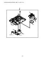
Page 44: ... 44 CD MECHANISM EXPLODED VIEW 1 1 DTA11T3C A M2 PIN 3 SW1 MOTOR C B 4 3 2 1 ...


